EP0352159B1 - Frequency drift tolerant method and device for demodulating constant envelope and continuous phase signals angularly modulated by a series of binary symbols - Google Patents
Frequency drift tolerant method and device for demodulating constant envelope and continuous phase signals angularly modulated by a series of binary symbols Download PDFInfo
- Publication number
- EP0352159B1 EP0352159B1 EP89401886A EP89401886A EP0352159B1 EP 0352159 B1 EP0352159 B1 EP 0352159B1 EP 89401886 A EP89401886 A EP 89401886A EP 89401886 A EP89401886 A EP 89401886A EP 0352159 B1 EP0352159 B1 EP 0352159B1
- Authority
- EP
- European Patent Office
- Prior art keywords
- phase
- bits
- differential phases
- phases
- differential
- Prior art date
- Legal status (The legal status is an assumption and is not a legal conclusion. Google has not performed a legal analysis and makes no representation as to the accuracy of the status listed.)
- Expired - Lifetime
Links
Images


Classifications
-
- H—ELECTRICITY
- H04—ELECTRIC COMMUNICATION TECHNIQUE
- H04L—TRANSMISSION OF DIGITAL INFORMATION, e.g. TELEGRAPHIC COMMUNICATION
- H04L27/00—Modulated-carrier systems
- H04L27/10—Frequency-modulated carrier systems, i.e. using frequency-shift keying
- H04L27/14—Demodulator circuits; Receiver circuits
Definitions
- the invention relates to the demodulation of binary information signals transmitted by angular modulation of a carrier, and more particularly relates to a method, and the corresponding device, for demodulation of signals with constant envelope and continuous phase angularly modulated by a train of binary symbols, in English "CPM” modulation for "continuous phase modulation", tolerating large frequency drifts.
- Constant envelope modulations are widely used today in radiocommunications because of their immunity to nonlinear amplitude distortions.
- Frequency modulation with continuous phase in which the phase variation due to a binary element can be spread over several bit periods has interesting properties with regard to the rather reduced spectral congestion.
- the demodulation is carried out either in a coherent demodulator, with a phase reference, by discriminator, or in a non-coherent demodulator which can be of differential type.
- each stage allows the transmission of a certain number of bits, ie n b .
- the modulation applied is an angular modulation with continuous phase, the imperfection of the transmission channel, the very significant "Doppler” frequency drifts when the demodulator is on board (for example on an airplane), the instability of the oscillators of the reception chain, etc. ... disturb the signal. These different degradations result in frequency drifts.
- the method according to the invention consists in performing digital processing in baseband, on the phase of the oversampled signal with respect to the bit period. This process assumes stage synchronization acquired, and it proceeds to demodulate the bits by jointly establishing bit synchronization and phase estimation, then correction of frequency drifts.
- the continuous phase angular demodulation method (and the corresponding device) according to the invention allows correct demodulation even in the presence of strong frequency drifts, with sensitivity performances of the same order as those obtained when the frequency drift is zero, while remaining compatible with frequency hopping links, even when each level at constant frequency has few bits.
- the invention also relates to a demodulation device intended for the implementation of this method.
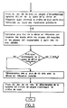
- the demodulation method according to the invention is carried out as follows, according to the flow diagram represented in FIGS. 1 to 3:
- the signal received by the receiver is amplified and filtered, then brought back into baseband by conventional means; the phase ⁇ of the signal collected at the output of this processing chain is sampled at a frequency F e at least twice greater than the bit frequency so as to verify the Nyquist criterion, and such that the number of samples q taken during a bit period T b is greater than a fraction k of the bit period T b corresponding to the bit synchronization error allowed, more or less.
- Each of the q classes of n b differential phases constitutes "a sampling comb", each corresponding to equidistant moments of possible decisions.
- Each comb is identified by the class number 1 to q it represents.
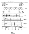
- FIG. 4 gives a digital example of the constitution of sampling combs.
- These sampling combs are offset one from the next by a sampling period.
- the sampling instants, for a level, and these combs are represented in FIG. 4 with the 4 original instants of the calculation of the differential phases constituting them.
- the next step is to "equalize" the qs. n b differential phases thus classified, if necessary (it is for this reason that the corresponding frame on the flow diagram of FIG. 1 is shown in dotted lines).
- certain angular modulations for example the continuous phase frequency modulations called “partial response”, produce phase variations over the duration of a symbol period which depend on several bits; the contribution to the phase variation due to this spread over several bits, assimilated to inter-symbol interference, must be reduced as much as possible before demodulation to allow decision-making. This reduction is obtained by the "equalization" operation which can be interpreted as the search for the symbol that generated the phase variation.
- the next step in the demodulation process consists in correcting the measured phases by assuming that the frequency drift is equal to one of several predefined frequency drifts, distributed to cover the whole range of possible drift. From the evaluation of an expression translating a noise minimization criterion, the supposed bits transmitted under the envisaged conditions are demodulated.
- the values of the predefined frequency drifts are chosen in a number such that the total processing does not occupy too long a time, but makes it possible to scan the most probable possibilities of frequency drifts and to quickly arrive at a good estimate of the real drift. .
- This processing step can be summarized succinctly as follows: a predefined frequency drift value being retained, the equalized differential phases of each of the q sampling combs are reduced by the variation in equalized phase corresponding to the frequency drift envisaged: the sign of the resulting differential phases provides the supposed bit transmitted.
- the predefined frequency drift values are such that the phase rotation generated by these errors must not produce too many erroneous decisions for the evaluation of the noise power: in fact, by the play of a predefined frequency drift, the equalized differential phase sees its sign reverse, the "decision" on the supposed value of the bit is then wrong.
- each set of n b bits makes it possible to calculate the assumed differential phases generated on transmission, that is to say to perform a reconstruction of the assumed differential phases transmitted which would correspond to this set of bits and to evaluate a "noise criterion" as a function of the reconstructed differential phases, of the measured differential phases, and of the assumed drift.
- the next step then consists in choosing the most appropriate frequency drift and set of samples, by minimizing the evaluated noise criterion. This selection can be made first for each drift value between the q possible games, then between the selected games associated with the different drift values. A more precise estimation of the frequency drift is then carried out, step B, from the reconstructed differential phases and the differential phases measured for the set of bits resulting from the selection.
- the last step consists in demodulating the q sets of differential phases (equalized), after correction of these differential phases as a function of the frequency drift estimated more precisely in the previous phase, then in selecting the resulting set of n b bits which minimizes the noise criterion calculated as above by associating with it the corresponding sampling comb which simultaneously gives bit synchronization.
- this last step can only be carried out if the frequency drift is deemed to be estimated with sufficient precision.
- a test intended to verify it is carried out as shown in FIG. 3. If this is not the case, the method can resume at step "A", from a set of predefined drifts distributed in a more close around the estimated drift after the first treatment.
- FIGS. 5 and 6 represent sub-assemblies of the demodulation device.
- FIG. 5 represents a first part of the demodulator.
- the reception chain comprises the HF reception antenna, followed by the HF reception stage, 1, amplifier and filter, followed by the intermediate frequency transposition stage, 2.
- the signal thus transposed into an intermediate frequency is applied to the input of the differential phase generation device 10 which includes a phase measurement circuit, 11 providing a continuous signal characteristic of the phase of the signal applied to its input.
- the output signal of this difference circuit 12 is therefore a continuous signal from which the elementary differential phases d ⁇ i can be taken between instants separated by a sampling period, by means of a sampler 14 controlled by a signal.
- sampling clock H e from a logic control circuit 40 shown in FIG. 6.
- the elementary differential phases resulting from this sampling are transmitted to the input of a delay line 15 with q stages.
- the samples stored in this delay line are transmitted, during the sampling period to an adder 16 which calculates the successive differential phases D ⁇ n corresponding to the phase variations over a period of 1 bit, by shifting each calculation of a sample , by the play of the offset in the delay line.
- the parasitic terms are at least of order 2 in z and z ⁇ 1.
- the demodulator shown in FIG. 5 includes an equalization device 20 corresponding to a modulation in which the phase variation over a period of 1 bit is spread over 3 bits of information.
- This equalization device 20 comprises 2 delay lines of duration equal to 1 bit, 21 and 22 in series; the input of the delay line 21 is connected to a first input of a multiplier 23 whose second input receives information relating to a multiplication coefficient K1.
- the outputs of the delay lines 21 and 22 are respectively connected to the inputs of two multipliers 24 and 25, the other inputs of which receive multiplier coefficients K2 and K3 respectively.
- These coefficients K1 K2 and K3 are directly related to the coefficients - ⁇ , +1, and - ⁇ of the equalization polynomial E (z).
- a referral system 30 makes it possible to constitute the "combs" defined above from the series of equalized phase differential values at the output of the equalization device, these equalized phases being emitted at the rate of the samples.
- This switching device comprises a first cyclic switch with q positions, 31, operating at the rate of the sampling clock H e , and which makes it possible to switch all the equalized differential phases assigned to the same modulo number q, towards the one of q memories, 32 (1), 32 (2) ... 32 (q).
- the outputs of these q memories are connected to corresponding inputs of a switching device 33 with q inputs and an output which is controlled at the rate of the clock bit H b obtained by frequency division by q of the clock d sampling H e in the control circuit 40 (FIG. 6).
- This switching device 33 makes it possible to transfer the equalized differential phases E ⁇ stored in one of the q memories, in packets of n b , and to process them as will be explained below.
- the device carrying out the rest of the processing is shown in FIG. 6: it comprises the logic control circuit 40 which controls the resetting to zero, the writing and reading of the memories, the selection of the frequency drift values, and the switches . To simplify the figure, the corresponding control wires have not been shown. It also comprises a generator of equalized differential phases associated with the predefined frequency drifts, 50, a difference circuit 60, a first input of which is connected to the output of the switching device 33 and the other input of which is connected to the output of the differential phase generator associated with the predefined frequency drifts 50, and which generates the corrected differential phases for each predefined frequency drift value.
- circuit 60 The output of circuit 60 is connected to a decision circuit + 1 / -1, which from each corrected differential phase value decides the value of the corresponding bit assumed to be sent.
- the corresponding decided bit sequences are then stored in one of q memories 72 (1), 72 (2) ... 72 (q) via a cyclic switch with q positions 71, the outputs of these memories being connected to the inputs a switching device with q inputs and 1 output, 73.
- the difference circuit 75 calculates the difference (E ⁇ k ) m - (E ⁇ k ) r - ⁇ ⁇ and a quadratic detector 76 in calculates the square. This detector is followed by an adder 77 which adds this value to the previous value transmitted to an accumulator 78 and reapplied to the adder 77, so as to calculate the noise criterion corresponding to a series of n b decided bits.
- This accumulator is connected to a logic comparison circuit 79, associated with a memory for storing the best result, 80, which compares, for each series of decided bits, the noise criterion calculated with the noise criterion previously stored and the store in its place if it is lower.
- the set of n b bits thus retained is the sequence of the n b bits assumed to be transmitted, available on the "decided bits" output.
- the preserved sampling comb constitutes bit synchronization, each of the instants composing this comb proving to be the best decision time;
- the predefined frequency value adopted turns out to be a rough estimate of the frequency drift.
- FIG. 7 represents the error rate curves as a function of this ratio for different values of uncorrected frequency drifts, 0, 1600 Hz, 3200 Hz, obtained by a conventional demodulation method in the case of an SRC4 demodulation, characterized by a modulation speed of 36 Kbits per second and for a frequency hopping link comprising 18 bits per level.
- the curve obtained by the demodulation method according to the invention with the maximum frequency error previously considered, ie 3200 Hz. It appears that the proposed demodulation method leads to degraded performance only by 1 '' order of 1 dB in the presence of strong frequency drifts compared to the performances obtained in an ideal case in the absence of frequency drift.
- the invention is not limited to the embodiments precisely described and shown.
- the entire demodulation method and device have been described, taking into account the necessary equalization only in the event of intersymbol interference.
- this equalization is not necessary, and the values of predefined frequency drifts result in phase variations which can be deduced directly from the measured differential phases, of course without equalization.
Description
L'invention se rapporte à la démodulation de signaux d'information binaires transmis par modulation angulaire d'une porteuse, et a plus particulièrement pour objet un procédé, et le dispositif correspondant, de démodulation de signaux à enveloppe constante et phase continue modulés angulairement par un train de symboles binaires, en anglais modulation "CPM" pour "continuous phase modulation", tolérant les dérives de fréquence importantes.The invention relates to the demodulation of binary information signals transmitted by angular modulation of a carrier, and more particularly relates to a method, and the corresponding device, for demodulation of signals with constant envelope and continuous phase angularly modulated by a train of binary symbols, in English "CPM" modulation for "continuous phase modulation", tolerating large frequency drifts.
Les modulations à enveloppe constante sont largement utilisées actuellement dans les radiocommunications du fait de leur immunité aux distorsions non linéaires d'amplitude. La modulation de fréquence à phase continue, dans laquelle la variation de phase due à un élément binaire peut être étalée sur plusieurs périodes bits présente des propriétés intéressantes en ce qui concerne l'encombrement spectral, assez réduit.Constant envelope modulations are widely used today in radiocommunications because of their immunity to nonlinear amplitude distortions. Frequency modulation with continuous phase, in which the phase variation due to a binary element can be spread over several bit periods has interesting properties with regard to the rather reduced spectral congestion.
Classiquement la démodulation est réalisée soit dans un démodulateur cohérent, avec une référence de phase, par discriminateur, soit dans un démodulateur non cohérent qui peut être de type différentiel.Conventionally, the demodulation is carried out either in a coherent demodulator, with a phase reference, by discriminator, or in a non-coherent demodulator which can be of differential type.
D'une manière générale, on sait effectuer la démodulation de signaux analogiques modulés en phase par des circuits entièrement numériques, en échantillonnant le signal reçu et en traitant les échantillons résultants, comme décrit par exemple dans un brevet US n° 3 938 052.In general, it is known to carry out the demodulation of analog signals modulated in phase by entirely digital circuits, by sampling the received signal and by processing the resulting samples, as described for example in US Pat. No. 3,938,052.
Lorsque le canal de transmission est dit "à sauts de fréquence", c'est-à-dire lorsque la fréquence de la porteuse varie par paliers, selon une séquence pseudo-aléatoire, les paliers étant de durée fixe, chaque palier permet la transmission d'un certain nombre de bits, soit nb. Lorsque de plus la modulation appliquée est une modulation angulaire à phase continue, l'imperfection du canal de transmission, les dérives en fréquence "Doppler" très importantes lorsque le démodulateur est embarqué (par exemple sur un avion), l'instabilité des oscillateurs de la chaîne de réception, etc... perturbent le signal. Ces différentes dégradations se traduisent par des dérives en fréquence.When the transmission channel is said to be "frequency hopping", that is to say when the carrier frequency varies in stages, according to a pseudo-random sequence, the stages being of fixed duration, each stage allows the transmission of a certain number of bits, ie n b . When, moreover, the modulation applied is an angular modulation with continuous phase, the imperfection of the transmission channel, the very significant "Doppler" frequency drifts when the demodulator is on board (for example on an airplane), the instability of the oscillators of the reception chain, etc. ... disturb the signal. These different degradations result in frequency drifts.
L'effet de ces dérives en fréquence, sur des signaux à enveloppe constante et phase continue modulés angulairement par un train de symboles binaires, est d'ajouter une composante continue aux signaux utiles traités. Avec un dispositif de démodulation à seuil fixe, la composante continue produit un décalage du diagramme de l'oeil par rapport à son niveau nominal, accroissant ainsi le taux d'erreur par bit. Un dispositif de démodulation utilisant un filtrage passe haut est mis en défaut par les suites de bit identiques, et cette situation se produit avec un grande probabilité dans les liaisons à sauts de fréquence avec des paliers courts et donc peu de bits par palier. Les techniques de démodulation par phase différentielle ou par discriminateur ne sont donc pas applicables en présence de fortes dérives de fréquence.The effect of these frequency drifts, on signals with constant envelope and continuous phase angularly modulated by a train of binary symbols, is to add a continuous component to the useful signals processed. With a fixed threshold demodulation device, the DC component produces an offset of the eye diagram from its nominal level, thus increasing the error rate per bit. A demodulation device using high-pass filtering is faulted by the identical bit sequences, and this situation occurs with a high probability in frequency-hopping links with short steps and therefore few bits per step. The demodulation techniques by differential phase or by discriminator are therefore not applicable in the presence of strong frequency drifts.
Le procédé selon l'invention consiste à effectuer des traitements numériques en bande de base, sur la phase du signal suréchantillonnée par rapport à la période bit. Ce procédé suppose acquise la synchronisation palier, et il procède à la démodulation des bits en établissant conjointement la synchronisation bit et l'estimation de phase, puis la correction des dérives en fréquence.The method according to the invention consists in performing digital processing in baseband, on the phase of the oversampled signal with respect to the bit period. This process assumes stage synchronization acquired, and it proceeds to demodulate the bits by jointly establishing bit synchronization and phase estimation, then correction of frequency drifts.
Le procédé (et le dispositif correspondant) de démodulation angulaire à phase continue selon l'invention permet une démodulation correcte même en présence de fortes dérives en fréquence, avec des performances en sensibilité du même ordre que celles obtenues lorsque la dérive en fréquence est nulle, tout en restant compatible avec les liaisons à sauts de fréquence, même lorsque chaque palier à fréquence constante comporte peu de bits.The continuous phase angular demodulation method (and the corresponding device) according to the invention allows correct demodulation even in the presence of strong frequency drifts, with sensitivity performances of the same order as those obtained when the frequency drift is zero, while remaining compatible with frequency hopping links, even when each level at constant frequency has few bits.
Selon l'invention un procédé de démodulation de signaux à enveloppe constante et phase continue consistant à effectuer un traitement numérique, par paliers de nb bits, d'un signal reçu ramené en bande de base dont la phase est suréchantillonnée par rapport à la période bit Tb, est caractérisé en ce qu'il consiste :
- dans une première phase, à mesurer q sous-ensembles de nb phases différentielles à la période bit, à partir d'instants de départ décalés les uns par rapport aux autres de fractions Tb/q de cette période pour former des peignes d'échantillonnage à la période bit décalés,
- dans une deuxième phase, à corriger a priori ces sous-ensembles de phases différentielles par des écarts de phase associés à un ensemble de d dérives en fréquence prédéfinies, pour générer d.q ensembles de nb phases différentielles corrigées, et à en déduire d.q jeux de nb bits démodulés associés ;
- dans une troisième phase, à reconstituer les phases différentielles supposées émises à partir de chacun des jeux de nb bits démodulés, et à calculer pour chacun des d.q jeux de bits démodulés un critère de bruit tenant compte du jeu de phases différentielles reconstituées et du jeu de phases différentielles mesurées et corrigées en fonction d'une dérive prédéfinie,
- dans une quatrième phase, à sélectionner le jeu de nb bits qui minimise le critère de bruit, la dérive en fréquence prédéfinie qui lui est associée correspondant à une estimation grossière de la dérive réelle,
- dans une avant-dernière phase, à partir du jeu de bits démodulé sélectionné, à calculer une estimation fine de la dérive réelle par moyenne des écarts entre les phases différentielles mesurées et les phases différentielles reconstituées associées à ce jeu de nb bits,
- et dans une dernière phase à effectuer une démodulation des q jeux de phases différentielles après les avoir corrigés de l'écart de phase associé à l'estimation fine de la dérive réelle, à calculer pour chacun le critère de bruit, et à sélectionner parmi les jeux de bits résultant celui qui minimise le critère de bruit, le peigne d'échantillonnage qui lui est associé constituant la synchronisation bit.
- in a first phase, to measure q subsets of n b differential phases in the bit period, from starting instants offset from each other by fractions T b / q of this period to form combs of sampling at the bit shifted period,
- in a second phase, to correct a priori these subsets of differential phases by phase differences associated with a set of d predefined frequency drifts, to generate dq sets of n b corrected differential phases, and to deduce therefrom dq sets of n b associated demodulated bits;
- in a third phase, to reconstruct the assumed differential phases emitted from each of the sets of n b demodulated bits, and to calculate for each of the dq sets of demodulated bits a noise criterion taking into account the set of reconstructed differential phases and the set differential phases measured and corrected according to a predefined drift,
- in a fourth phase, to select the set of n b bits which minimizes the noise criterion, the predefined frequency drift associated with it corresponding to a rough estimate of the real drift,
- in a penultimate phase, from the selected demodulated bit set, to calculate a fine estimate of the real drift by average of the differences between the measured differential phases and the reconstructed differential phases associated with this set of n b bits,
- and in a last phase to demodulate the q sets of differential phases after having corrected them for the phase difference associated with the fine estimation of the real drift, to calculate for each the noise criterion, and to select from the bit sets resulting the one which minimizes the noise criterion, the sampling comb associated with it constituting bit synchronization.
L'invention a également pour objet un dispositif de démodulation destiné à la mise en oeuvre de ce procédé.The invention also relates to a demodulation device intended for the implementation of this method.
L'invention sera mieux comprise et d'autres caractéristiques apparaîtront à l'aide de la description qui suit en référence aux figures annexées.
- Les figures 1, 2 et 3 forment l'organigramme du procédé de démodulation selon l'invention ;
- La figure 4 est un schéma illustrant l'échantillonnage de la variation de phase du signal reçu et la formation des "peignes" d'échantillonnage associés ;
- Les figures 5 et 6 représentent des schémas fonctionnels de deux parties du dispositif de démodulation selon l'invention ;
- La figure 7 représente des courbes de variation du taux d'erreur en fonction du rapport signal sur bruit pour différentes valeurs de dérives en fréquence, et selon que le procédé selon l'invention est ou n'est pas utilisé.
- Figures 1, 2 and 3 form the flow diagram of the demodulation method according to the invention;
- FIG. 4 is a diagram illustrating the sampling of the phase variation of the received signal and the formation of the associated sampling "combs";
- FIGS. 5 and 6 represent functional diagrams of two parts of the demodulation device according to the invention;
- FIG. 7 represents curves of variation of the error rate as a function of the signal to noise ratio for different values of frequency drifts, and according to whether the method according to the invention is or is not used.
Le procédé de démodulation selon l'invention s'effectue de la manière suivante, suivant l'organigramme représenté sur les figures 1 à 3 :The demodulation method according to the invention is carried out as follows, according to the flow diagram represented in FIGS. 1 to 3:
Le signal reçu par le récepteur est amplifié et filtré, puis ramené en bande de base par des moyens conventionnels ; la phase φ du signal recueilli en sortie de cette chaîne de traitement est échantillonnée à une fréquence Fe au moins deux fois supérieure à la fréquence bit de façon à vérifier le critère de Nyquist, et telle que le nombre d'échantillons q prélevés pendant une période bit Tb soit supérieur à une fraction k de la période bit Tb correspondant à l'erreur de synchronisation bit admise, en plus ou en moins. Il est donc nécessaire de prélever des échantillons avant l'instant supposé de l'arrivée du premier bit du palier et après l'instant supposé de la fin du dernier bit de la séquence des nb bits d'un palier, en nombre égal à (2E(q/k)+1), E(q/k) désignant la partie entière de q/k. Sont donc disponibles après échantillonnage (q . nb + 2E(q/k)+1) échantillons de phase du signal.The signal received by the receiver is amplified and filtered, then brought back into baseband by conventional means; the phase φ of the signal collected at the output of this processing chain is sampled at a frequency F e at least twice greater than the bit frequency so as to verify the Nyquist criterion, and such that the number of samples q taken during a bit period T b is greater than a fraction k of the bit period T b corresponding to the bit synchronization error allowed, more or less. It is therefore necessary to take samples before the supposed instant of the arrival of the first bit of the plateau and after the supposed instant of the end of the last bit of the sequence of the n b bits of a plateau, in number equal to (2E (q / k) +1), E (q / k) denoting the integer part of q / k. Are therefore available after sampling (q. N b + 2E (q / k) +1) signal phase samples.
Pour chaque nouvel échantillon, à un instant d'échantillonnage nTe, une phase différentielle élémentaire dφn-1 correspondant à la variation de phase du signal entre l'échantillon prélevé n et l'échantillon immédiatement précédent, n-1, est calculée. Ainsi, il existe q . nb + 2E(q/k) phases différentielles élémentaires dφn pour un palier.For each new sample, at a sampling instant nTe, an elementary differential phase dφ n-1 corresponding to the phase variation of the signal between the sampled sample n and the immediately preceding sample, n-1, is calculated. So there is q. n b + 2E (q / k) elementary differential phases dφ n for a bearing.
A partir de cet ensemble de phases différentielles élémentaires, des peignes d'échantillonnage sont construits de la manière suivante :
- une origine des temps pour chaque palier est définie par l'instant du premier échantillon t₁ ;
- à partir de cet instant d'origine, les q phases différentielles élémentaires dφ₁,...dφq qui suivent sont additionnées de façon à calculer la phase différentielle Dφ₁ correspondant à une variation de phase sur une période de 1 bit ;
- puis à partir de l'instant du deuxième échantillon t₂ une autre addition est effectuée pour les q phases différentielles élémentaires suivantes Dφ₂ = dφ₂ +..+dφq+1 etc..,

- an origin of the times for each level is defined by the instant of the first sample t₁;
- from this initial instant, the q elementary differential phases dφ₁, ... dφ q which follow are added so as to calculate the differential phase Dφ₁ corresponding to a phase variation over a period of 1 bit;
- then from the time of the second sample t₂ another addition is made for the following q elementary differential phases Dφ₂ = dφ₂ + .. + dφ q + 1 etc ..,
Chacune des q classes de nb phases différentielles constitue "un peigne d'échantillonnage", chacun correspondant à des instants équidistants de décisions possibles. Chaque peigne est identifié par le numéro de la classe 1 à q qu'il représente.Each of the q classes of n b differential phases constitutes "a sampling comb", each corresponding to equidistant moments of possible decisions. Each comb is identified by the
La figure 4 donne un exemple numérique de constitution de peignes d'échantillonnage. Dans cet exemple un palier comporte nb = 5 bits, et la synchronisation bit est connue à ± Tb/2 (k = 2). La période d'échantillonnage est telle que q = 4 échantillons sont prélevés pendant une période bit ; si Te est la période d'échantillonnage, la période bit est Tb = 4Te. Il y a donc (4 x 5 + 2 E(4/2)+1) = 25 échantillons de phase du signal sur un palier ; 24 phases différentielles élémentaires dφi, i = 1 à 24 sont donc calculées et 4 peignes d'échantillonnage constitués chacun de 5 phases différentielles Dφi correspondant aux variations de phase successives sur des intervalles de durée égale à la période bit sont créés. Ces peignes d'échantillonnage sont décalés l'un par rapport au suivant d'une période d'échantillonnage. Les instants d'échantillonnage, pour un palier, et ces peignes sont représentés sur la figure 4 avec les 4 instants d'origine du calcul des phases différentielles les constituant.FIG. 4 gives a digital example of the constitution of sampling combs. In this example, a level has n b = 5 bits, and the bit synchronization is known to ± T b / 2 (k = 2). The sampling period is such that q = 4 samples are taken during a bit period; if T e is the sampling period, the bit period is T b = 4T e . There are therefore (4 x 5 + 2 E (4/2) +1) = 25 signal phase samples on a level; 24 elementary differential phases dφ i , i = 1 to 24 are therefore calculated and 4 sampling combs each consisting of 5 differential phases Dφ i corresponding to the successive phase variations over intervals of duration equal to the bit period are created. These sampling combs are offset one from the next by a sampling period. The sampling instants, for a level, and these combs are represented in FIG. 4 with the 4 original instants of the calculation of the differential phases constituting them.
L'étape suivante consiste à "égaliser" les q . nb phases différentielles ainsi classées, si nécessaire (c'est pour cette raison que le cadre correspondant sur l'organigramme de la figure 1 est représenté en pointillés). En effet, certaines modulations angulaires, par exemple les modulations de fréquence à phase continue dites "à réponse partielle", produisent des variations de phase sur la durée d'une période symbole qui dépendent de plusieurs bits ; la contribution à la variation de phase due à cet étalement sur plusieurs bits, assimilée à de l'interférence inter symboles, doit être autant que possible réduite avant la démodulation pour permettre la prise de décision. Cette réduction est obtenue par l'opération "d'égalisation" qui peut être interprétée comme la recherche du symbole ayant généré la variation de phase.The next step is to "equalize" the qs. n b differential phases thus classified, if necessary (it is for this reason that the corresponding frame on the flow diagram of FIG. 1 is shown in dotted lines). Indeed, certain angular modulations, for example the continuous phase frequency modulations called "partial response", produce phase variations over the duration of a symbol period which depend on several bits; the contribution to the phase variation due to this spread over several bits, assimilated to inter-symbol interference, must be reduced as much as possible before demodulation to allow decision-making. This reduction is obtained by the "equalization" operation which can be interpreted as the search for the symbol that generated the phase variation.
Cette égalisation n'est appliquée que lorsque la phase différentielle sur une période symbole dépend de plusieurs bits du fait de la modulation, ou de toute autre cause provoquant de l'interférence intersymbole, par exemple, un filtrage non idéal. Elle sera décrite plus en détails ci-après.This equalization is only applied when the differential phase over a symbol period depends on several bits due to modulation, or any other cause causing intersymbol interference, for example, non-ideal filtering. It will be described in more detail below.
L'étape suivante du procédé de démodulation, illustrée à partir du point A de l'organigramme sur la figure 2, consiste à corriger les phases mesurées en supposant que la dérive de fréquence est égale à l'une de plusieurs dérives de fréquence prédéfinies, réparties pour couvrir toute la gamme de dérive possible. A partir de l'évaluation d'une expression traduisant un critère de minimisation du bruit, les bits supposés émis dans les conditions envisagées sont démodulés. Les valeurs des dérives en fréquence prédéfinies sont choisies en nombre tel que le traitement total n'occupe pas un temps trop long, mais permette de balayer les possibilités les plus probables de dérives en fréquence et de parvenir rapidement à une bonne estimation de la dérive réelle. Cette étape du traitement, décrite plus en détails ci-après, peut être résumée succinctement de la manière suivante : une valeur de dérive en fréquence prédéfinie étant retenue, les phases différentielles égalisées de chacun des q peignes d'échantillonnage sont diminuées de la variation de phase égalisée correspondant à la dérive de fréquence envisagée : le signe des phases différentielles résultantes fournit le bit supposé émis. Les valeurs de dérives en fréquence prédéfinies sont telles que la rotation de phase engendrée par ces erreurs ne doit pas produire trop de décisions erronées pour l'évaluation de la puissance de bruit : en effet, par le jeu d'une dérive en fréquence prédéfinie, la phase différentielle égalisée voit son signe s'inverser, la "décision" sur la valeur supposée du bit est alors erronée.The next step in the demodulation process, illustrated from point A of the flow diagram in FIG. 2, consists in correcting the measured phases by assuming that the frequency drift is equal to one of several predefined frequency drifts, distributed to cover the whole range of possible drift. From the evaluation of an expression translating a noise minimization criterion, the supposed bits transmitted under the envisaged conditions are demodulated. The values of the predefined frequency drifts are chosen in a number such that the total processing does not occupy too long a time, but makes it possible to scan the most probable possibilities of frequency drifts and to quickly arrive at a good estimate of the real drift. . This processing step, described in more detail below, can be summarized succinctly as follows: a predefined frequency drift value being retained, the equalized differential phases of each of the q sampling combs are reduced by the variation in equalized phase corresponding to the frequency drift envisaged: the sign of the resulting differential phases provides the supposed bit transmitted. The predefined frequency drift values are such that the phase rotation generated by these errors must not produce too many erroneous decisions for the evaluation of the noise power: in fact, by the play of a predefined frequency drift, the equalized differential phase sees its sign reverse, the "decision" on the supposed value of the bit is then wrong.
A l'issue de cette étape de traitement il existe donc q jeux de nb bits, correspondant aux q peignes d'échantillonnage, pour chaque valeur de dérive en fréquence prédéfinie ; chaque jeu de nb bits permet alors de calculer des phases différentielles supposées engendrées à l'émission, c'est-à-dire d'effectuer une reconstitution des phases différentielles supposées émises qui correspondraient à ce jeu de bits et d'évaluer un "critère de bruit" fonction des phases différentielles reconstituées, des phases différentielles mesurées, et de la dérive supposée.At the end of this processing step, there are therefore q sets of n b bits, corresponding to the q sampling combs, for each value of drift in predefined frequency; each set of n b bits then makes it possible to calculate the assumed differential phases generated on transmission, that is to say to perform a reconstruction of the assumed differential phases transmitted which would correspond to this set of bits and to evaluate a "noise criterion" as a function of the reconstructed differential phases, of the measured differential phases, and of the assumed drift.
L'étape suivante consiste alors à choisir la dérive de fréquence et le jeu d'échantillons les plus appropriés, par la minimisation du critère de bruit évalué. Cette sélection peut se faire d'abord pour chaque valeur de dérive entre les q jeux possibles, puis entre les jeux sélectionnés associés aux différentes valeurs de dérive. Une estimation plus précise de la dérive de fréquence est alors effectuée, étape B, à partir des phases différentielles reconstituées et des phases différentielles mesurées pour le jeu de bits issu de la sélection.The next step then consists in choosing the most appropriate frequency drift and set of samples, by minimizing the evaluated noise criterion. This selection can be made first for each drift value between the q possible games, then between the selected games associated with the different drift values. A more precise estimation of the frequency drift is then carried out, step B, from the reconstructed differential phases and the differential phases measured for the set of bits resulting from the selection.
Enfin, la dernière étape consiste à démoduler les q ensembles de phases différentielles (égalisées), après correction de ces phases différentielles en fonction de la dérive de fréquence estimée plus précisément dans la phase précédente, puis à sélectionner le jeu de nb bits résultant qui minimise le critère de bruit calculé comme précédemment en lui associant le peigne d'échantillonnage correspondant qui donne simultanément la synchronisation bit.Finally, the last step consists in demodulating the q sets of differential phases (equalized), after correction of these differential phases as a function of the frequency drift estimated more precisely in the previous phase, then in selecting the resulting set of n b bits which minimizes the noise criterion calculated as above by associating with it the corresponding sampling comb which simultaneously gives bit synchronization.
Bien entendu, cette dernière étape peut n'être effectuée qui si la dérive de fréquence est jugée estimée avec une précision suffisante. Un test destiné à le vérifier est effectué comme représenté sur la figure 3. Si ce n'est pas le cas, le procédé peut reprendre à l'étape "A", à partir d'un ensemble de dérives prédéfinies réparties dans une gamme plus étroite autour de la dérive estimée à l'issue du premier traitement.Of course, this last step can only be carried out if the frequency drift is deemed to be estimated with sufficient precision. A test intended to verify it is carried out as shown in FIG. 3. If this is not the case, the method can resume at step "A", from a set of predefined drifts distributed in a more close around the estimated drift after the first treatment.
Ces différentes étapes vont être décrites plus en détails ci-après, en liaison avec les figures 5 et 6 qui représentent des sous-ensembles du dispositif de démodulation.These different steps will be described in more detail below, in conjunction with FIGS. 5 and 6 which represent sub-assemblies of the demodulation device.
La figure 5 représente une première partie du démodulateur. La chaîne de réception comporte l'antenne de réception HF, suivie de l'étage de réception HF,1, amplificateur et filtre, suivi de l'étage de transposition en fréquence intermédiaire, 2. Le signal ainsi transposé en fréquence intermédiaire est appliqué à l'entrée du dispositif de génération de phases différentielles 10 qui comporte un circuit de mesure de phase, 11 fournissant un signal continu caractéristique de la phase du signal appliqué à son entrée. Ce signal est appliqué aux entrées d'un circuit de différence, 12, respectivement par une voie directe et par une voie comportant un circuit à retard 13 qui impose un retard égal à la période d'échantillonnage Te = Tb/q. Le signal de sortie de ce circuit de différence 12 est donc un signal continu à partir duquel peuvent être prélevées les phases différentielles élémentaires dφi entre des instants séparés d'une période d'échantillonnage, au moyen d'un échantillonneur 14 commandé par un signal d'horloge d'échantillonnage He issu d'un circuit logique de commande 40 représenté sur la figure 6. Les phases différentielles élémentaires résultant de cet échantillonnage sont transmises à l'entrée d'une ligne à retard 15 à q étages. Les échantillons stockés dans cette ligne à retard sont transmis, à la période d'échantillonnage à un sommateur 16 qui calcule les phases différentielles successives Dφn correspondant aux variations de phase sur une période de 1 bit,en décalant à chaque calcul d'un échantillon, par le jeu du décalage dans la ligne à retard.FIG. 5 represents a first part of the demodulator. The reception chain comprises the HF reception antenna, followed by the HF reception stage, 1, amplifier and filter, followed by the intermediate frequency transposition stage, 2. The signal thus transposed into an intermediate frequency is applied to the input of the differential
Si la modulation employée et le filtrage à la réception génèrent des interférences intersymboles connues à priori, comme indiqué ci-dessus une étape d'égalisation est mise en oeuvre. Si l'on suppose par exemple que trois bits d'informations contribuent à une variation de phase différentielle sur une période de 1 bit, et si l'on considère qu'aucun bruit ni aucune dérive en fréquence ne modifie cette phase différentielle, celle-ci peut se mettre sous la forme :![]()
désignent les bits d'informations et valent ±1, A, B, C étant des coefficients constants. Selon la théorie des transformées en "z", l'expression ci-dessus se traduit par le polynôme P(z) défini comme suit :![]()
L'égaliseur résulte du polynôme E(z) qui vérifie l'expression P(z).E(z) = 1, puisque par définition l'égalisation correspond à la recherche de l'inverse du polynôme P. Ce polynôme n'est pas causal et donc non réalisable physiquement mais il peut être approximé de la manière suivante :![]()
α et β sont deux constantes déterminées à partir des coefficients A, B et C en annulant les termes en z-1.z du polynôme P(z).E(z). Ainsi les termes parasites sont au moins d'ordre 2 en z et z⁻¹. Ces techniques d'égalisation sont connues et l'on suppose donc dans la suite que les coefficients α et β de l'égaliseur ont été préalablement calculés. (Si plus de trois bits génèrent la variation de phase exprimée ci-dessus et si l'on cherche à égaliser à un ordre plus élevé que l'ordre 2 en ajoutant les puissances désirées au terme en z⁻¹z, il est nécessaire de calculer un plus grand nombre de coefficients.)If the modulation used and the filtering on reception generate intersymbol interference known a priori, as indicated above, an equalization step is implemented. If, for example, it is assumed that three bits of information contribute to a differential phase variation over a period of 1 bit, and if it is considered that no noise or no frequency drift modifies this differential phase, this this can be in the form: ![]()
denote the information bits and have the value ± 1, A, B, C being constant coefficients. According to the theory of transforms into "z", the above expression results in the polynomial P (z) defined as follows: ![]()
The equalizer results from the polynomial E (z) which satisfies the expression P (z) .E (z) = 1, since by definition the equalization corresponds to the search for the inverse of the polynomial P. This polynomial is not not causal and therefore not physically achievable but it can be approximated as follows: ![]()
α and β are two constants determined from the coefficients A, B and C by canceling the terms in z -1. z of the polynomial P (z) .E (z). Thus the parasitic terms are at least of
Pour l'égalisation, le démodulateur représenté sur la figure 5 comporte un dispositif d'égalisation 20 correspondant à une modulation dans laquelle la variation de phase sur une période de 1 bit est étalée sur 3 bits d'information. Ce dispositif d'égalisation 20 comporte 2 lignes à retard de durée égale à 1 bit, 21 et 22 en série ; l'entrée de la ligne à retard 21 est reliée à une première entrée d'un multiplieur 23 dont la seconde entrée reçoit une information relative à un coefficient de multiplication K₁. De même les sorties des lignes à retard 21 et 22 sont respectivement reliées aux entrées de deux multiplicateurs 24 et 25 dont les autres entrées reçoivent respectivement des coefficients multiplicateurs K₂ et K₃. Ces coefficients K₁ K₂ et K₃ sont directement liés aux coefficients -α, +1, et -β du polynôme d'égalisation E(z). Les sorties de ces trois multiplicateurs sont reliées à l'entrée d'un sommateur 26 qui fournit donc une phase différentielle dite "égalisée", Eφ, en principe liée seulement à la valeur du bit d'information de rang correspondant. La sortie de ce sommateur est la sortie du dispositif d'égalisation. Bien entendu l'égalisation ne peut être réalisée de manière correcte que si les variations de phase sont suffisamment connues et qu'elles peuvent être modélisées linéairement par rapport aux bits d'informations qui la génèrent.For equalization, the demodulator shown in FIG. 5 includes an
Un système d'aiguillage 30 permet de constituer les "peignes" définis ci-dessus à partir de la suite de valeurs différentielles de phase égalisées en sortie du dispositif d'égalisation, ces phases égalisées étant émises au rythme des échantillons. Ce dispositif d'aiguillage comporte un premier commutateur cyclique à q positions, 31, fonctionnant au rythme de l'horloge d'échantillonnage He, et qui permet d'aiguiller toutes les phases différentielles égalisées affectées du même numéro modulo q, vers l'une de q mémoires, 32(1), 32(2)...32(q). Les sorties de ces q mémoires sont reliées à des entrées correspondantes d'un dispositif d'aiguillage 33 à q entrées et une sortie qui est commandé au rythme de l'horloge bit Hb obtenu par division de fréquence par q de l'horloge d'échantillonnage He dans le circuit de commande 40 (figure 6). Ce dispositif d'aiguillage 33 permet de transférer les phases différentielles égalisées Eφ mémorisées dans l'une des q mémoires, par paquets de nb, et les traiter comme il sera expliqué ci-après.A
Le dispositif réalisant la suite du traitement est représenté sur la figure 6 : il comporte le circuit logique de commande 40 qui commande la remise à zéro, l'écriture et la lecture des mémoires, la sélection des valeurs de dérive en fréquence, et les commutateurs. Pour simplifier la figure, les fils de commande correspondants n'ont pas été représentés. Il comporte également un générateur de phases différentielles égalisées associées aux dérives en fréquence prédéfinies,50, un circuit de différence 60 dont une première entrée est reliée à la sortie du dispositif d'aiguillage 33 et dont l'autre entrée est reliée à la sortie du générateur de phases différentielles associées aux dérives en fréquence prédéfinies 50, et qui génère les phases différentielles corrigées pour chaque valeur de dérive en fréquence prédéfinie.The device carrying out the rest of the processing is shown in FIG. 6: it comprises the
La sortie du circuit 60 est reliée à un circuit 65 de décision +1/-1, qui à partir de chaque valeur de phase différentielle corrigée décide la valeur du bit correspondant supposé émis. Les suites de bits décidés correspondantes sont alors mémorisés dans l'une de q mémoires 72(1), 72(2)...72(q) via un commutateur cyclique à q positions 71, les sorties de ces mémoires étant reliées aux entrées d'un dispositif d'aiguillage à q entrées et 1 sortie, 73.The output of
Ces mêmes suites de bits décidés sont transmises à un circuit 74 de reconstitution des phases différentielles égalisées supposées émises compte tenu des bits décidés. Ces valeurs de phases différentielles sont alors transmises à un circuit de différence 75 qui les compare aux valeurs correspondantes mesurées, après égalisation, disponibles à la sortie du circuit de différence 60.These same sequences of decided bits are transmitted to a
Il est alors possible d'évaluer pour chaque jeu de nb bits, la moyenne des écarts quadratiques entre les phases différentielles mesurées et égalisées, et les phases différentielles égalisées reconstituées à partir des nb bits correspondants et de la dérive en fréquence prédéfinie. En réalité cela revient à évaluer l'écart quadratique moyen du "bruit" affectant la séquence de nb bits, si aucune erreur n'était commise lors de l'évaluation des phases différentielles émises. L'expression de la moyenne des écarts quadratiques, qui est le critère "de bruit", est la suivante :

où (Eφk)m est la phase différentielle égalisée mesurée (disponible en sortie du circuit 30), (Eφk)r est la phase différentielle égalisée reconstituée à partir du jeu de bits sélectionné (disponible en sortie du circuit de reconstitution 74) et ε φ est la phase différentielle égalisée due à la dérive de fréquence (disponible en sortie du générateur 50).It is then possible to evaluate, for each set of n b bits, the average of the quadratic differences between the measured and equalized differential phases, and the equalized differential phases reconstructed from the corresponding n b bits and the predefined frequency drift. In reality, this amounts to evaluating the mean square deviation of the "noise" affecting the sequence of n b bits, if no error was made during the evaluation of the differential phases transmitted. The expression for the mean of the quadratic deviations, which is the "noise" criterion, is as follows:
where (Eφ k ) m is the equalized differential phase measured (available at the output of circuit 30), (Eφ k ) r is the equalized differential phase reconstructed from the selected bit set (available at output of reconstruction circuit 74) and ε φ is the equalized differential phase due to the frequency drift (available at the output of generator 50).
Pour un bit de rang k dans une suite de nb bits, k compris entre 1 et nb, le circuit de différence 75 calcule la différence (Eφk)m-(Eφk)r- ε φ et un détecteur quadratique 76 en calcule le carré. Ce détecteur est suivi d'un additionneur 77 qui additionne cette valeurs à la valeur précédente transmise à un accumulateur 78 et réappliquée à l'additionneur 77, de façon à calculer le critère de bruit correspondant à une suite de nb bits décidés. La sortie de cet accumulateur est reliée à un circuit logique de comparaison 79, associé à une mémoire de stockage du meilleur résultat, 80, qui compare, pour chaque suite de bits décidés, le critère de bruit calculé au critère de bruit précédemment stocké et le stocke à sa place s'il est inférieur.For a bit of rank k in a sequence of n b bits, k between 1 and n b , the
Pour l'évaluation de ce critère, et durant tout le procédé, on suppose que la dérive est constante sur la durée d'un palier. Le processus de décision est donc le suivant : seul le jeu de nb bits pour lequel le critère est minimum, ainsi que le numéro d'identification du peigne d'échantillonnage correspondant sont retenus. Ce choix d'un jeu de nb bits et du peigne d'échantillonnage correspondant est effectué autant de fois qu'il y a de valeurs de dérive en fréquence prédéfinies, soit d fois.For the evaluation of this criterion, and throughout the process, it is assumed that the drift is constant over the duration of a plateau. The decision process is therefore as follows: only the set of n b bits for which the criterion is minimum, as well as the identification number of the corresponding sampling comb are retained. This choice of a set of n b bits and of the corresponding sampling comb is made as many times as there are predefined frequency drift values, ie d times.
Le critère du minimum de l'écart quadratique moyen, qui a servi à sélectionner l'un de tous les jeux de bits et des peignes d'échantillonnage associés pour une même valeur de dérive en fréquence prédéfinie, est appliqué de nouveau aux couples (jeux de nb bits, numéros de peignes d'échantillonnage) précédemment sélectionnés et correspondant chacun à une valeur de dérive en fréquence prédéfinie. A l'issue de ce traitement il ne demeure qu'un seul jeu de nb bits et un seul peigne d'échantillonnage, associés à une valeur de dérive en fréquence prédéfinie.The criterion of the minimum of the mean square deviation, which was used to select one of all the sets of bits and of the associated sampling combs for the same value of drift in predefined frequency, is applied again to the couples (sets of n b bits, sample comb numbers) previously selected and each corresponding to a predefined frequency drift value. At the end of this processing, there remains only a single set of n b bits and a single sampling comb, associated with a predefined frequency drift value.
Le jeu de nb bits ainsi retenu est la séquence des nb bits supposée émise, disponible sur la sortie "bits décidés".The set of n b bits thus retained is the sequence of the n b bits assumed to be transmitted, available on the "decided bits" output.
Le peigne d'échantillonnage conservé constitue la synchronisation bit, chacun des instants composant ce peigne s'avérant être le meilleur instant de décision ;The preserved sampling comb constitutes bit synchronization, each of the instants composing this comb proving to be the best decision time;
La valeur en fréquence prédéfinie retenue se révèle être une estimation grossière de la dérive en fréquence.The predefined frequency value adopted turns out to be a rough estimate of the frequency drift.
Comme indiqué ci-dessus, en moyennant nb différences entre les phases différentielles "reçues" mesurées et égalisées, soient (Eφk)m, et les phases différentielles égalisées reconstituées soient (Eφk)r à partir du jeu des nb décidés, on obtient une estimation fine de la dérive en fréquence "réelle". Suivant la précision exigée pour le démodulateur, cette estimation peut être suffisante. Dans le cas contraire, comme indiqué ci-dessus, il est possible de répéter les traitements exposés ci-dessus jusqu'à l'obtention de la précision souhaitée en les appliquant à un ou plusieurs autres ensembles de valeurs de dérives en fréquence, réparties autour de l'estimation "grossière" de la dérive définie dans la phase précédente. Il faut cependant noter que la méthode converge rapidement et que bien souvent un seul traitement de ce type conduit à une précision suffisante sur la valeur de la dérive en fréquence.As indicated above, by making n b differences between the measured and equalized "received" differential phases, let (Eφ k ) m , and the reconstituted equalized differential phases be (Eφ k ) r from the set of decided n b , a fine estimate of the "real" frequency drift is obtained. Depending on the precision required for the demodulator, this estimate may be sufficient. Otherwise, as indicated above, it is possible to repeat the treatments described above until the desired precision is obtained by applying them to one or more other sets of frequency drift values, distributed around the "rough" estimate of the drift defined in the previous phase. It should however be noted that the method converges quickly and that very often a single processing of this type leads to sufficient precision on the value of the frequency drift.
Enfin, lorsque la dérive en fréquence est estimée avec suffisamment de précision, les traitements effectués précédemment pour une valeur de dérive prédéfinie sont répétés avec cette "valeur fine" de dérive pour fournir finalement les nb bits décidés, et la synchronisation bit correspondante.Finally, when the frequency drift is estimated with sufficient precision, the processing carried out previously for a predefined drift value is repeated with this "fine value" of drift to finally supply the n b bits decided, and the corresponding bit synchronization.
L'évaluation des performances de ce procédé de démodulation a été faite en mesurant le taux d'erreur par bit en fonction du rapport signal sur bruit Eb/N₀, Eb désignant l'énergie par bit, et N₀ la densité de bruit.The performance of this demodulation process was evaluated by measuring the error rate per bit as a function of the signal to noise ratio E b / N₀, E b denoting the energy per bit, and N₀ the noise density.
La figure 7 représente les courbes de taux d'erreur en fonction de ce rapport pour différentes valeurs de dérives en fréquence non corrigées, 0, 1600 Hz, 3200 Hz, obtenues par un procédé de démodulation classique dans le cas d'une démodulation SRC4, caractérisée par une vitesse de modulation de 36 Kbits par seconde et pour une liaison à sauts de fréquence comportant 18 bits par palier. Sur la même figure a été également représentée la courbe obtenue par le procédé de démodulation selon l'invention, avec l'erreur en fréquence maximale considérée précédemment soit 3200 Hz. Il apparaît que le procédé de démodulation proposé conduit à des performances dégradées seulement de l'ordre de 1 dB en présence de fortes dérives en fréquences par rapport aux performances obtenues dans un cas idéal en l'absence de dérive en fréquence.FIG. 7 represents the error rate curves as a function of this ratio for different values of uncorrected frequency drifts, 0, 1600 Hz, 3200 Hz, obtained by a conventional demodulation method in the case of an SRC4 demodulation, characterized by a modulation speed of 36 Kbits per second and for a frequency hopping link comprising 18 bits per level. In the same figure has also been shown the curve obtained by the demodulation method according to the invention, with the maximum frequency error previously considered, ie 3200 Hz. It appears that the proposed demodulation method leads to degraded performance only by 1 '' order of 1 dB in the presence of strong frequency drifts compared to the performances obtained in an ideal case in the absence of frequency drift.
L'invention n'est pas limitée aux modes de réalisation précisément décrits et représentés. En particulier on a décrit l'ensemble du procédé et du dispositif de démodulation en tenant compte d'une égalisation nécessaire seulement en cas d'interférence intersymbole. Bien entendu si la variation de phase due à un bit n'est pas étalée, cette égalisation n'est pas nécessaire, et les valeurs de dérives en fréquence prédéfinies se traduisent par des variations de phase qui peuvent être déduites directement des phases différentielles mesurées, bien entendu sans égalisation.The invention is not limited to the embodiments precisely described and shown. In particular, the entire demodulation method and device have been described, taking into account the necessary equalization only in the event of intersymbol interference. Of course if the phase variation due to a bit is not spread out, this equalization is not necessary, and the values of predefined frequency drifts result in phase variations which can be deduced directly from the measured differential phases, of course without equalization.
De plus, pour représenter d'une manière explicite le démodulateur, la représentation qui en a été faite montre des blocs fonctionnels. Bien entendu l'ensemble des fonctions correspondantes peut être traité au moyen d'un microprocesseur.In addition, to represent the demodulator explicitly, the representation which has been made of it shows functional blocks. Of course, all of the corresponding functions can be processed by means of a microprocessor.
Claims (8)
- Method for demodulating constant envelope and continuous phase signals consisting in carrying out a digital processing, in batches of nb bits, of a received signal reduced to baseband whose phase is oversampled with respect to the bit period Tb, characterised in that it consists:- in a first phase in measuring q sub-sets of nb differential phases at the bit period, from starting instants shifted with respect to one another by fractions Tb/q of this period in order to form, at the bit period, shifted sampling combs,- in a second phase, in correcting these sub-sets of differential phases a priori through phase deviations associated with a set of d predefined frequency drifts, in order to generate d.q sets of nb corrected differential phases, and in deducing therefrom d.q collections of nb associated demodulated bits;- in a third phase, in reconstituting the supposedly transmitted differential phases from each of the collections of nb demodulated bits, and in calculating for each of the d.q collections of demodulated bits a noise criterion taking account of the collection of reconstituted differential phases and for the collection of measured and corrected differential phases as a function of a predefined drift,- in a fourth phase, in selecting the collection of nb bits which minimises the noise criterion, the predefined frequency drift which is associated therewith corresponding to a rough estimation of the true drift,- in a penultimate phase, on the basis of the selected demodulated collection of bits, in calculating a fine estimation of the true drift by averaging the deviations between the measured differential phases and the reconstituted differential phases associated with this collection of nb bits,- and in a last phase, in carrying out a demodulation of the q collections of differential phases after having corrected them by the phase deviation associated with the fine estimation of the true drift, in calculating for each one the noise criterion and in selecting from the resulting collections of bits the one which minimises the noise criterion, the sampling comb which is associated therewith constituting the bit synchronisation.
- Method according to Claim 1, characterised in that, the phase variation due to a bit being spread over several bit periods of the transmitted signal, the measured differential phases are equalised in the first phase in order to reduce the spread effect, all the phase deviations associated with the predefined frequency drifts, then the reconstituted differential phases determined during the processing being equalised in the same way.
- Method according to one of Claims 1 and 2, characterised in that, in order to calculate the q subsets of nb differential phases at the bit period, the method consists in sampling the baseband signal at the period Tb/q, in measuring the elementary differential phase variations between successive samples, and in summing nb times q successive elementary differential phases from a starting sample in order to form a sub-set of nb differential phases, the other sub-sets being obtained in the same way after shifting at the start of a sample.
- Method according to one of Claims 1 and 2, characterised in that the d predefined frequency drifts are distributed within the possible range of frequency drift.
- Method according to Claim 4, characterised in that, at the end of the fourth phase, a test is carried out on the accuracy of the rough estimation of the true drift and in that if the accuracy is inadequate, the method is resumed at its second phase on the basis of another set of predefined frequency drifts distributed about the previously adopted rough estimation.
- Method according to one of Claims 1 and 2, characterised in that for a collection of demodulated bits taking account of a frequency drift, the noise criterion is the average of the quadratic deviations between the measured differential phases corrected by the phase deviation associated with this frequency drift, and the corresponding reconstituted differential phases.
- Device for demodulating constant envelope and continuous phase signals, intended for implementing the method according to one of the preceding claims, characterised in that it includes, controlled by a control circuit (40):- a circuit (10) for measuring q sub-sets of nb differential phases on the basis of a signal, characteristic of the phase of a received signal to be demodulated, sampled at the period Tb/q,- a circuit (20) for equalising the differential phases carrying out a linear combination of successive differential phases, if necessary, in order to reduce the spread effect when it exists,- a circuit (30) for routing and for storage in order to constitute sub-sets of measured and equalised differential phases corresponding to sampling combs shifted by bit period fractions,- a generator (50) of equalised differential phases which are associated with the set of predefined frequency drifts,- a difference circuit (60) connected to the outputs of the routing and storage circuit (30) and of the generator (50),- a decision circuit (65) with regard to the value of bits, having an output connected, on the one hand, to a circuit for routing and for storing demodulated bits and, on the other hand, to a circuit (74) for reconstituting the supposedly transmitted phases as a function of these bits,- a circuit for calculating a noise criterion (75-78) connected to the output of the difference circuit (60) and to that of the circuit for reconstituting the supposedly transmitted phases (74),- and a comparison circuit with memory (79, 80) for selecting from the collections of stored bits, the one which minimises the noise criterion.
- Demodulating device according to Claim 7, characterised in that the functions for control, for calculation, for storage, for decision and for selection are implemented in a microprocessor which processes the digital values of differential phases.
Applications Claiming Priority (2)
| Application Number | Priority Date | Filing Date | Title |
|---|---|---|---|
| FR8809731 | 1988-07-19 | ||
| FR8809731A FR2635420B1 (en) | 1988-07-19 | 1988-07-19 | METHOD AND DEVICE FOR DEMODULATING SIGNALS WITH A CONSTANT ENVELOPE AND A CONTINUOUS PHASE ANGULARLY MODULATED BY A TRAIN OF BINARY SYMBOLS, TOLERATING THE FREQUENCY DERIVATIVES |
Publications (2)
| Publication Number | Publication Date |
|---|---|
| EP0352159A1 EP0352159A1 (en) | 1990-01-24 |
| EP0352159B1 true EP0352159B1 (en) | 1993-08-04 |
Family
ID=9368540
Family Applications (1)
| Application Number | Title | Priority Date | Filing Date |
|---|---|---|---|
| EP89401886A Expired - Lifetime EP0352159B1 (en) | 1988-07-19 | 1989-06-30 | Frequency drift tolerant method and device for demodulating constant envelope and continuous phase signals angularly modulated by a series of binary symbols |
Country Status (4)
| Country | Link |
|---|---|
| US (1) | US4945312A (en) |
| EP (1) | EP0352159B1 (en) |
| DE (1) | DE68908038T2 (en) |
| FR (1) | FR2635420B1 (en) |
Families Citing this family (14)
| Publication number | Priority date | Publication date | Assignee | Title |
|---|---|---|---|---|
| US5228062A (en) * | 1990-04-16 | 1993-07-13 | Telebit Corporation | Method and apparatus for correcting for clock and carrier frequency offset, and phase jitter in multicarrier modems |
| US5141764A (en) * | 1990-07-24 | 1992-08-25 | Conagra, Inc. | Wheat milling process |
| US5194287A (en) * | 1990-07-24 | 1993-03-16 | Conagra, Inc. | Wheat milling process and milled wheat product |
| FR2735872B1 (en) * | 1995-06-23 | 1997-08-08 | Thomson Csf | NAVIGATION SYSTEM FOR REAL-TIME COORDINATION OF MOVING MOBILE EVOLVING WITHOUT DIRECT VIEW |
| US6212245B1 (en) * | 1995-07-13 | 2001-04-03 | Canon Kabushiki Kaisha | Communication apparatus |
| FR2738383B1 (en) * | 1995-09-05 | 1997-10-03 | Thomson Csf | METHOD FOR VECTOR QUANTIFICATION OF LOW FLOW VOCODERS |
| FR2743893B1 (en) * | 1996-01-23 | 1998-03-06 | Thomson Csf | RADIOCOMMUNICATION AND LOCATION DEVICE |
| US5812604A (en) * | 1996-07-16 | 1998-09-22 | Scientific-Atlanta, Inc. | Constant envelope continuous phase frequency shift key modulation apparatus and method at radio frequencies |
| FR2758673B1 (en) * | 1997-01-21 | 1999-04-23 | Thomson Csf | SELF-ADAPTIVE DATA TRANSMISSION METHOD AND IMPLEMENTING DEVICE |
| FR2778041A1 (en) * | 1998-04-24 | 1999-10-29 | Thomson Csf | Power transmitter tube dynamic compensation method |
| FR2788390B1 (en) | 1999-01-12 | 2003-05-30 | Thomson Csf | HIGH EFFICIENCY SHORTWAVE BROADCAST TRANSMITTER OPTIMIZED FOR DIGITAL TYPE TRANSMISSIONS |
| FR2790343B1 (en) | 1999-02-26 | 2001-06-01 | Thomson Csf | SYSTEM FOR ESTIMATING THE COMPLEX GAIN OF A TRANSMISSION CHANNEL |
| FR2799592B1 (en) | 1999-10-12 | 2003-09-26 | Thomson Csf | SIMPLE AND SYSTEMATIC CONSTRUCTION AND CODING METHOD OF LDPC CODES |
| US6700928B1 (en) | 2000-05-11 | 2004-03-02 | The Boeing Company | Tetrahedron modem |
Family Cites Families (1)
| Publication number | Priority date | Publication date | Assignee | Title |
|---|---|---|---|---|
| US3938052A (en) * | 1974-05-09 | 1976-02-10 | Teletype Corporation | Digital demodulator for phase-modulated waveforms |
-
1988
- 1988-07-19 FR FR8809731A patent/FR2635420B1/en not_active Expired - Lifetime
-
1989
- 1989-06-30 EP EP89401886A patent/EP0352159B1/en not_active Expired - Lifetime
- 1989-06-30 DE DE89401886T patent/DE68908038T2/en not_active Expired - Fee Related
- 1989-07-17 US US07/380,537 patent/US4945312A/en not_active Expired - Fee Related
Also Published As
| Publication number | Publication date |
|---|---|
| EP0352159A1 (en) | 1990-01-24 |
| FR2635420B1 (en) | 1990-10-19 |
| US4945312A (en) | 1990-07-31 |
| DE68908038D1 (en) | 1993-09-09 |
| FR2635420A1 (en) | 1990-02-16 |
| DE68908038T2 (en) | 1993-11-18 |
Similar Documents
| Publication | Publication Date | Title |
|---|---|---|
| EP0125722B1 (en) | Circuit for joint adaptive equalisation and demodulation | |
| EP0352159B1 (en) | Frequency drift tolerant method and device for demodulating constant envelope and continuous phase signals angularly modulated by a series of binary symbols | |
| EP0036084B1 (en) | Process and device for the control of the initial adjustment of the clock of a receiver for synchronous data | |
| EP0013343B1 (en) | Process and device to detect a pseudo-random sequence of 0 degree and 180 degree phase changes of the carrier in a data receiver | |
| FR2623669A1 (en) | EQUALIZATION APPARATUS AND METHOD FOR DATA TRANSMISSION | |
| EP0178720A1 (en) | Circuit arrangement for the reception of digital data with an adaptive clock recovery circuit | |
| EP0329537A1 (en) | Transmission system using MSK modulation and coherent differential detection | |
| EP0113487A1 (en) | Method to be used in an echo cancelling arrangement for measuring an echo delay, and arrangement for carrying out this method | |
| EP0017716B1 (en) | Method for initializing an adaptive equalizer starting from an unknown data signal in a transmission system using a double side band modulation with quadrature carriers | |
| EP2915302B9 (en) | Method and apparatus for demodulating q-ary gfsk signals | |
| EP0762703A1 (en) | Multicarrier demodulation with reduction of white frequency distortion | |
| EP0376250B1 (en) | Self-adaptive equalization device for a differentially coherent demodulation arrangement | |
| EP0073869A1 (en) | Data receiving apparatus with listener echo canceller | |
| EP0808043A1 (en) | A system for detecting the presence of a numerical signal carrier wave and a receiver including such a system | |
| EP0230900B1 (en) | Device for clock recovery | |
| FR2794589A1 (en) | ITERATIVE TDMA RADIO TRANSMISSION METHOD | |
| FR2546011A1 (en) | METHOD FOR NON-COHERENT DEMODULATION OF A CONSTANTLY CONSTANT SYMBOL-BASED ENERGY MODULE SIGNAL AND DEMODULATOR FOR CARRYING OUT SAID METHOD | |
| EP0080544B1 (en) | Method for receiving a data signal with double side-band quadrature carrier modulation | |
| EP0039980A1 (en) | Adaptive digital data receiving system with compensation of the amplitude and phase distortions introduced by the data transmission channel | |
| CA1312657C (en) | Shifted four state phase modulation synchronisation device | |
| EP0035295B1 (en) | Clock phase control method for a digital data receiving system, phase recovery circuit for carrying out this method and digital data receiving system comprising this circuit | |
| EP0094040B1 (en) | System for synchronous data transmission with the aid of a constant envelope amplitude-modulated carrier | |
| EP0792053A1 (en) | Digital transmission system using continuous phase modulation | |
| EP0127544B1 (en) | Echo canceller with an adaptive digital filter for a transmission system | |
| FR2786965A1 (en) | SIGNAL CARRIER RECOVERY METHOD |
Legal Events
| Date | Code | Title | Description |
|---|---|---|---|
| PUAI | Public reference made under article 153(3) epc to a published international application that has entered the european phase |
Free format text: ORIGINAL CODE: 0009012 |
|
| AK | Designated contracting states |
Kind code of ref document: A1 Designated state(s): DE GB IT |
|
| 17P | Request for examination filed |
Effective date: 19900621 |
|
| 17Q | First examination report despatched |
Effective date: 19920708 |
|
| GRAA | (expected) grant |
Free format text: ORIGINAL CODE: 0009210 |
|
| AK | Designated contracting states |
Kind code of ref document: B1 Designated state(s): DE GB IT |
|
| ITF | It: translation for a ep patent filed |
Owner name: JACOBACCI CASETTA & PERANI S.P.A. |
|
| REF | Corresponds to: |
Ref document number: 68908038 Country of ref document: DE Date of ref document: 19930909 |
|
| GBT | Gb: translation of ep patent filed (gb section 77(6)(a)/1977) |
Effective date: 19931014 |
|
| RAP2 | Party data changed (patent owner data changed or rights of a patent transferred) |
Owner name: THOMSON-CSF |
|
| PGFP | Annual fee paid to national office [announced via postgrant information from national office to epo] |
Ref country code: GB Payment date: 19940520 Year of fee payment: 6 Ref country code: DE Payment date: 19940520 Year of fee payment: 6 |
|
| PLBE | No opposition filed within time limit |
Free format text: ORIGINAL CODE: 0009261 |
|
| STAA | Information on the status of an ep patent application or granted ep patent |
Free format text: STATUS: NO OPPOSITION FILED WITHIN TIME LIMIT |
|
| 26N | No opposition filed | ||
| PG25 | Lapsed in a contracting state [announced via postgrant information from national office to epo] |
Ref country code: GB Effective date: 19950630 |
|
| GBPC | Gb: european patent ceased through non-payment of renewal fee |
Effective date: 19950630 |
|
| PG25 | Lapsed in a contracting state [announced via postgrant information from national office to epo] |
Ref country code: DE Effective date: 19960301 |
|
| PG25 | Lapsed in a contracting state [announced via postgrant information from national office to epo] |
Ref country code: IT Free format text: LAPSE BECAUSE OF NON-PAYMENT OF DUE FEES;WARNING: LAPSES OF ITALIAN PATENTS WITH EFFECTIVE DATE BEFORE 2007 MAY HAVE OCCURRED AT ANY TIME BEFORE 2007. THE CORRECT EFFECTIVE DATE MAY BE DIFFERENT FROM THE ONE RECORDED. Effective date: 20050630 |