EP0351749A2 - Method of manufacturing semiconductor devices, and leadframe and differential overlapping apparatus therefor - Google Patents
Method of manufacturing semiconductor devices, and leadframe and differential overlapping apparatus therefor Download PDFInfo
- Publication number
- EP0351749A2 EP0351749A2 EP89113056A EP89113056A EP0351749A2 EP 0351749 A2 EP0351749 A2 EP 0351749A2 EP 89113056 A EP89113056 A EP 89113056A EP 89113056 A EP89113056 A EP 89113056A EP 0351749 A2 EP0351749 A2 EP 0351749A2
- Authority
- EP
- European Patent Office
- Prior art keywords
- leadframe
- longitudinal
- band
- leads
- group
- Prior art date
- Legal status (The legal status is an assumption and is not a legal conclusion. Google has not performed a legal analysis and makes no representation as to the accuracy of the status listed.)
- Granted
Links
Images


Classifications
-
- H—ELECTRICITY
- H10—SEMICONDUCTOR DEVICES; ELECTRIC SOLID-STATE DEVICES NOT OTHERWISE PROVIDED FOR
- H10W—GENERIC PACKAGES, INTERCONNECTIONS, CONNECTORS OR OTHER CONSTRUCTIONAL DETAILS OF DEVICES COVERED BY CLASS H10
- H10W70/00—Package substrates; Interposers; Redistribution layers [RDL]
- H10W70/01—Manufacture or treatment
- H10W70/04—Manufacture or treatment of leadframes
-
- H—ELECTRICITY
- H10—SEMICONDUCTOR DEVICES; ELECTRIC SOLID-STATE DEVICES NOT OTHERWISE PROVIDED FOR
- H10W—GENERIC PACKAGES, INTERCONNECTIONS, CONNECTORS OR OTHER CONSTRUCTIONAL DETAILS OF DEVICES COVERED BY CLASS H10
- H10W70/00—Package substrates; Interposers; Redistribution layers [RDL]
- H10W70/01—Manufacture or treatment
- H10W70/04—Manufacture or treatment of leadframes
- H10W70/048—Mechanical treatments, e.g. punching, cutting, deforming or cold welding
-
- H—ELECTRICITY
- H10—SEMICONDUCTOR DEVICES; ELECTRIC SOLID-STATE DEVICES NOT OTHERWISE PROVIDED FOR
- H10P—GENERIC PROCESSES OR APPARATUS FOR THE MANUFACTURE OR TREATMENT OF DEVICES COVERED BY CLASS H10
- H10P72/00—Handling or holding of wafers, substrates or devices during manufacture or treatment thereof
- H10P72/04—Apparatus for manufacture or treatment
- H10P72/0438—Apparatus for making assemblies not otherwise provided for, e.g. package constructions
-
- H—ELECTRICITY
- H10—SEMICONDUCTOR DEVICES; ELECTRIC SOLID-STATE DEVICES NOT OTHERWISE PROVIDED FOR
- H10W—GENERIC PACKAGES, INTERCONNECTIONS, CONNECTORS OR OTHER CONSTRUCTIONAL DETAILS OF DEVICES COVERED BY CLASS H10
- H10W70/00—Package substrates; Interposers; Redistribution layers [RDL]
- H10W70/40—Leadframes
- H10W70/421—Shapes or dispositions
-
- H—ELECTRICITY
- H10—SEMICONDUCTOR DEVICES; ELECTRIC SOLID-STATE DEVICES NOT OTHERWISE PROVIDED FOR
- H10W—GENERIC PACKAGES, INTERCONNECTIONS, CONNECTORS OR OTHER CONSTRUCTIONAL DETAILS OF DEVICES COVERED BY CLASS H10
- H10W70/00—Package substrates; Interposers; Redistribution layers [RDL]
- H10W70/40—Leadframes
- H10W70/481—Leadframes for devices being provided for in groups H10D8/00 - H10D48/00
-
- H—ELECTRICITY
- H10—SEMICONDUCTOR DEVICES; ELECTRIC SOLID-STATE DEVICES NOT OTHERWISE PROVIDED FOR
- H10W—GENERIC PACKAGES, INTERCONNECTIONS, CONNECTORS OR OTHER CONSTRUCTIONAL DETAILS OF DEVICES COVERED BY CLASS H10
- H10W72/00—Interconnections or connectors in packages
-
- H—ELECTRICITY
- H10—SEMICONDUCTOR DEVICES; ELECTRIC SOLID-STATE DEVICES NOT OTHERWISE PROVIDED FOR
- H10W—GENERIC PACKAGES, INTERCONNECTIONS, CONNECTORS OR OTHER CONSTRUCTIONAL DETAILS OF DEVICES COVERED BY CLASS H10
- H10W90/00—Package configurations
- H10W90/811—Multiple chips on leadframes
-
- H—ELECTRICITY
- H10—SEMICONDUCTOR DEVICES; ELECTRIC SOLID-STATE DEVICES NOT OTHERWISE PROVIDED FOR
- H10W—GENERIC PACKAGES, INTERCONNECTIONS, CONNECTORS OR OTHER CONSTRUCTIONAL DETAILS OF DEVICES COVERED BY CLASS H10
- H10W74/00—Encapsulations, e.g. protective coatings
-
- Y—GENERAL TAGGING OF NEW TECHNOLOGICAL DEVELOPMENTS; GENERAL TAGGING OF CROSS-SECTIONAL TECHNOLOGIES SPANNING OVER SEVERAL SECTIONS OF THE IPC; TECHNICAL SUBJECTS COVERED BY FORMER USPC CROSS-REFERENCE ART COLLECTIONS [XRACs] AND DIGESTS
- Y10—TECHNICAL SUBJECTS COVERED BY FORMER USPC
- Y10T—TECHNICAL SUBJECTS COVERED BY FORMER US CLASSIFICATION
- Y10T29/00—Metal working
- Y10T29/49—Method of mechanical manufacture
- Y10T29/49002—Electrical device making
- Y10T29/49117—Conductor or circuit manufacturing
- Y10T29/49121—Beam lead frame or beam lead device
-
- Y—GENERAL TAGGING OF NEW TECHNOLOGICAL DEVELOPMENTS; GENERAL TAGGING OF CROSS-SECTIONAL TECHNOLOGIES SPANNING OVER SEVERAL SECTIONS OF THE IPC; TECHNICAL SUBJECTS COVERED BY FORMER USPC CROSS-REFERENCE ART COLLECTIONS [XRACs] AND DIGESTS
- Y10—TECHNICAL SUBJECTS COVERED BY FORMER USPC
- Y10T—TECHNICAL SUBJECTS COVERED BY FORMER US CLASSIFICATION
- Y10T29/00—Metal working
- Y10T29/53—Means to assemble or disassemble
- Y10T29/5313—Means to assemble electrical device
- Y10T29/53174—Means to fasten electrical component to wiring board, base, or substrate
- Y10T29/53178—Chip component
Definitions
- This invention relates to a method of manufacturing semiconductor devices from a continuous length of leadframe. It more particularly relates to a method of producing semiconductor devices of the type wherein each semiconductor chip is sandwiched between at least one pair of leads for bonding and encapsulated hermetically in a molded resinous body.
- the invention also relates to a leadframe and a differential overlapping mechanism for advantageously carrying out the method.
- a pair of parallel leadframes A, B respectively formed with aligned leads 2′, 3′ at a constant pitch P′ are transferred longitudinally thereof, as indicated by the arrows.
- semiconductor chips 1′ are bonded to the respective leads 2 of one leadframe A, as shown in Figure 16.
- the pair of leadframes A, B are brought closer to each other, so that the leads 3′ of the other leadframe B is overlapped on the chips 1′ for bonding thereto, as shown in Figure 17.
- each chip 1′ together with the associated leads 2′, 3′ is encapsulated in a molded resin body 4′ which is cut off from the respective leadframes A, B to provide an individual semiconductor product.
- the above prior art method is disadvantageous in that two separate leadframes A, B are required for production of semiconductor devices, thereby posing handling inconvenience (e.g. requiring two separate transfer guides, and etc.) in addition to involving material waste.
- the respective leads 2, 3, which are kept free as projecting are likely to come into contact with external objects particularly when the leadframes A, B are separately handled.
- the leads may be subjected to unacceptable deformation during the manufacturing process, consequently resulting in a higher chance of quality deterioration.
- an integral leadframe C which includes a pair of longitudinal bands C1, C2 connected together by bar-like connecting segments C3 spaced longitudinally of the leadframe at a constant pitch P ⁇ .
- One longitudinal band C1 is formed with a the leadframe and extend toward the other longitudinal band C2, whereas the other band C2 is formed with a group of shorter leads 3 ⁇ which are also spaced longitudinally of the leadframe but extend toward the one longitudinal band C1 in staggered relation to the group of longer leads 2 ⁇ .
- the integral leadframe C is transferred longitudinally thereof, as indicated by an arrow. During such transfer, a semiconductor chip 1 ⁇ is bonded to each shorter lead 3 ⁇ . Subsequently, a corresponding longer lead 2 ⁇ is bent along a bending line C4, so that the bent portion is overlapped on a corresponding chip 1 ⁇ . Finally, the chip together with the associated leads is hermetically molded in a resin body 4 ⁇ , and cut off from the leadframe to provide an individual semiconductor product.
- the method of Figure 18 is advantageous in that semiconductor devices can be produced from the single leadframe C which enables easier handling. Further, all of the leads 2 ⁇ , 3 ⁇ are always located in the same plane of the leadframe throughout various stages of the manufacturing process. Thus, the longitudinal space between the two longitudinal bands C1, C2 is an area always protected by these bands, so that the leads 2 ⁇ , 3 ⁇ arranged in this protected area are less likely to come into contact with external objects. Therefore, it is possible to avoid unexpected deformation of the leads, thereby improving the quality of the final products.
- each longer lead 2 ⁇ causes a weight increase of the individual semiconductor device in addition to involving material waste.
- each pair of leads 2 ⁇ , 3 ⁇ are spaced longitudinally of the leadframe C before and after the molding operation, so that the resulting product must necessarily have an increased width S which also causes a weight increase.
- this width increase also results in decrease in number of the products obtainable per unit length of the leadframe C, thus causing material waste.
- Another object of the present invention is to provide a leadframe which is particularly suitable for carrying out the method of the present invention.
- a further object of the present invention is to provide a differential overlapping mechanism or apparatus which can be advantageously used for carrying out the method of the present invention.
- Still another object of the present invention is to provide a modified leadframe which enables doubling of the productivity.
- Still further object of the present invention is to enable adjustment of the differential overlapping mechanism depending on the types or dimensions of leadframes to be used or the types or dimensions of semiconductor devices to be produced.
- Still further object of the present invention is to enable slip-free transfer of the leadframe through the differential overlapping mechanism.
- a method of manufacturing semiconductor devices from an elongated leadframe which comprises at least two transversely spaced longitudinal bands connected together by connecting segments spaced longitudinally of the leadframe, one longitudinal band being formed with a first group of leads spaced longitudinally of the leadframe and extending toward the other longitudinal band, the other longitudinal band being formed with a second group of leads spaced longitudinally of the leadframe and extending toward the one longitudinal band in staggered relation to the first group of leads, the method comprising the steps of: transferring the leadframe longitudinally thereof; bonding semiconductor chips to the first group of leads during transfer of the leadframe; causing the two bands to displace away from each other perpendicularly to a plane containing the leadframe; causing the two bands to move relative to each other longitudinally of the leadframe so that each lead of the first group assumes substantially the same longitudinal position as a corresponding lead of the second group; and causing the two bands to displace toward each other perpendicularly to the plane of the leadframe so that a semiconductor
- the leadframe to be used is an integral piece, so that it may be handled very conveniently throughout the entire manufacturing process with less likelihood of the individual leads being deformed by unexpected contact with external objects.
- the first group of leads and the second groups of leads are initially arranged in staggered relation.
- the two longitudinal bands are displaced relative to each other perpendicularly to the plane of the leadframe and longitudinally of the leadframe, so that the first group leads assume the same longitudinal positions as the second group leads with the individual semiconductor chips interposed therebetween.
- the resulting semiconductor products may have reduced width and weight, the width reduction also contributing to prevention of material waste and to enhancement of productivity.
- the method of the present invention requires no lateral bending of the leads.
- the leadframe may be transferred at a high speed, consequently realizing improved productivity and decreased production cost.
- the present invention also provides an improvement in the leadframe referred above in connection with the method. More specifically, the improvement of the leadframe resides in that each of the bar-like connecting segments has a pair of narrower neck portions for connection to the respective longitudinal bands.
- each bar-like connecting segment When the two longitudinal bands of the leadframe are displaced relative to each other longitudinally thereof, each bar-like connecting segment is deformed under a bending force. If the connecting segment has a constant width over its entire length, the bending force is evenly distributed throughout the segment which, for this reason, may be arcuately deformed within the elasticity limit. The connecting segment thus deformed acts as a spring tending to restore to its original state. Thus, the leadframe, which has been longitudinally deformed, may spring back to its original state after all external forces have been relieved, consequently giving adverse influences on subsequent procedure.
- each connecting segment has a pair of narrower neck portions which provide positions for stress concentration and easy deformation when the two longitudinal bands are displaced relative to each other longitudinally of the leadframe.
- the connecting segment is permanently deformed at these neck portions, thereby preventing or mitigating the unwanted spring-back phenomenon of the leadframe described above.
- the present invention further provides a differential overlapping apparatus which can be advantageously used for the method of the invention.
- the differential overlapping apparatus comprises: a first feed wheel arranged in a path of transfer of the leadframe and driven into rotation to have a specified circumferential speed, the first feed wheel having an outer circumference which provides a contact arc for coming into feeding contact with one longitudinal band of the leadframe; and a second feed wheel arranged in side-by-side relation to the first feed wheel and driven into rotation to have the same circumferential speed as the first feed wheel, the second feed wheel having an outer circumference which provides a contact arc for coming into contact with the other longitudinal band of the leadframe, the contact arc of the second feed wheel being longer than the contact arc of the first feed wheel and positioned radially outwardly thereof.
- the contact arc of the second feed wheel is longer than that of the first feed wheel.
- the two feed wheels are rotated to have the same circumferential speed, a particular length of the one longitudinal band passes through the first feed wheel within a shorter time than a corresponding length of the other longitudinal band passes through the second feed wheel.
- the one longitudinal band will have advanced relative to the other longitudinal band after passage through the respective feed wheels.
- the contact arc of the second feed wheel is located radially outside that of the first feed wheel, the two longitudinal bands are separated from each other perpendicularly to the plane of the leadframe. In this way, it is possible to overlap the leads of the one longitudinal band onto the counterpart leads of the other longitudinal band.
- the differential overlapping apparatus is advantageous in the simplicity of the arrangement because it requires only two feed wheels arranged in side-by-side relation. It is, of course, possible to combine the feed wheels with other mechanisms which would help the operation of differential overlapping, as described hereinafter.
- FIG. 1 there is shown a semiconductor device which can be advantageously manufactured from a leadframe according to the present invention.
- the semiconductor device is illustrated as being in the form of a diode which comprises a semiconductor chip 1 held in conduction with a pair of external leads 2, 3 and hermetically encapsulated in a molded resin body 4.
- the leadframe embodying the present invention is illustrated in Figures 3 and 4.
- This leadframe which is generally designated by reference numeral 10, includes a pair of longitudinal bands 11, 12 connected to each other by means of bar-like connecting segments 13.
- the leadframe may be formed from a metallic plate to have a suitable width W and a substantially continuous length.
- first band One longitudinal band 11 (hereafter referred to as “first band”) is integrally formed with leads 2 respectively arranged between the connecting segments 13.
- second band The other longitudinal band 12 (hereafter referred to as “second band”) is also formed with integral leads 3 in corresponding relation to the leads 2 of the first band to provide lead pairs arranged within the respective spaces between the connecting segments. Each pair of leads 2, 3 extend toward each other in staggered relation.
- each connecting segment 13 is spaced from each other longitudinally of the leadframe at a suitable pitch P.
- each connecting segment is inclined relative to the transverse direction of the leadframe 10, and has a pair of neck portions 14, 15 of a narrower width w for connection to the respective longitudinal bands 11, 12.
- the leadframe 10 is transferred longitudinally thereof, as indicated by an arrow F in Figure 5. During such transfer, semiconductor chips 1 are bonded onto the tips of the respective leads 2 of the first longitudinal band 11. Upon subsequent transfer, the leadframe is passed through a differential overlapping mechanism to be described below, whereby each pair of leads 2, 3 overlap each other, as illustrated in Figure 6.
- the differential overlapping mechanism which is arranged between a pair of guide rollers 16, 17 for longitudinally guiding the leadframe 10, comprises a diametrically larger feed wheel 18 and a diametrically smaller feed wheel 19.
- the two wheels 18, 19 are rotated in the same rotational direction R and at the same circumferential speed.
- the outer circumference of the larger feed wheel 18 is provided with equiangularly spaced engaging projections 18b for successive engagement with correspondingly spaced indexing holes 11a (see Figure 5) of the first longitudinal band 11.
- the outer circumference of the smaller wheel 19 is provided with equiangularly spaced engaging projections 19b for successive engagement with correspondingly spaced indexing holes 12a (see Figure 5) of the second longitudinal band 12.
- the leadframe 10 passes through the differential overlapping mechanism without slippage.
- the two wheels 18, 19 may be constituted by gears or sprockets.
- the larger feed wheel 18 comes into feeding contact with the first longitudinal band 11 of the leadframe 10 along a larger diameter arc
- the smaller feed wheel 19 comes into feeding contact with the second longitudinal band 12 of the leadframe along a smaller diameter arc.
- Both ends of the larger diameter arc are located substantially at the same positions as those of the smaller diameter arc.
- the smaller diameter arc is displaced radially outwardly of the larger diameter arc by the amount H, the former is larger in length than the latter.
- each lead 2 of the first longitudinal band 11 of the leadframe 10 displaces to a position under the corresponding lead 3 of the second longitudinal band 12 during passage of the leadframe through the feed wheels, as best illustrated in Figure 8.
- the lead 2 of the first longitudinal band 11 overlaps the corresponding lead 3 of the second longitudinal band 12 after complete passage over the feed wheels, as shown in Figures 6 and 9.
- each semiconductor chip 1 bonded in advance to the lead 2 may be bonded to the other (couterpart) lead 3 as a result of processing within the differential overlapping mechanism.
- the differential overlapping mechanism has two important functions. First, this mechanism causes the first longitudinal band 11 to slightly advance relative to the second longitudinal band 12 longitudinally of the leadframe 10. Second, the overlapping mechanism provides a level difference between the two longitudinal bands 11, 12 to enable overlapping between the pairs of leads 2, 3. It should be appreciated here that the relative longitudinal movement between the two longitudinal bands 11, 12 occurs only upon passage of the leadframe 10 through the overlapping mechanism but not before and after it because the two feed wheels 18, 19, though having different contact lengths, rotate at the same circumferential speed to feed the two longitudinal bands at the same speed as a whole.
- each connecting segment 13 is deformed when the two longitudinal bands 11, 12 are displaced relative to each other longitudinally of the leadframe 10.
- the narrower neck portions 14, 15 (figure 4) of the connecting segment 13 provide positions for stress concentration to ensure that the segment is permanently deformed at these positions to prevent subsequent spring-back phenomenon of the leadframe.
- the connecting segment 13 remains substantially straight as a whole even after such deformation.
- each connecting segment 13 is initially inclined relative to the transverse direction of the leadframe 10, as already described.
- the connecting segment is deformed to become perpendicular to the leadframe, as shown in Figure 6.
- the spaces between the respective connecting segments 13 become substantially rectangular to accommodate the respective molded resin bodies 4 which are subsequently formed within these spaces to become also rectangular.
- the pitch P (see Figure 3) may be made as small as possible to increase the number of semiconductor devices to be produced per unit length of the leadframe 10.
- each semiconductor device thus formed is separated from the leadframe 10 to provide the final product shown in Figures 1 and 2.
- the present invention is not limited to the particular leadframe 10 shown in Figures 3 to 6, wherein the two longitudinal bands 11, 12 are arranged to produce only one row of semiconductor devices.
- the leadframe may be modified to produce two or more rows of semiconductor devices.
- the modified leadframe 10′ has a central longitudinal band 12′ (second longitudinal band) on both sides of which are disposed a pair of side longitudinal bands 11′ (first longitudinal bands) to enable successive production of semiconductor devices in two rows, thereby doubling productivity.
- a differential overlapping mechanism suitable for such a leadframe may comprise a central smaller feed wheel for feeding contact with the central longitudinal band 12′, and a pair of larger feed wheels arranged on both sides of the central wheel to come into feeding contact with the side longitudinal bands 11′.
- Figures 11 to 14 show a modified differential overlapping mechanism according to the present invention.
- the modified overlapping mechanism which is arranged between a pair of guide rollers 16, 17 for longitudinally guiding the leadframe 10, comprises a smaller feed wheel 20 having a diameter d ( Figure 13), and a larger feed wheel 21 having a larger diameter D.
- the smaller feed wheel 20 drivingly rotated on a shaft 20a comes in feeding contact with the first longitudinal band 11 of the leadframe.
- the larger feed wheel 21, which is drivingly rotated on a shaft 21a coaxial with the other shaft 20a comes in feeding contact with the second longitudinal band 12.
- the smaller wheel 20 is rotated at a higher rotational speed than the larger wheel 21, so that these two wheels have the same circumferential speed.
- a first nipping roller mechanism 22 is disposed between the upstream guide roller 16 and the feed rollers 20, 21.
- a second nipping roller mechanism 23 is arranged between the downstream guide roller 17 and the feed rollers.
- the first nipping roller mechanism 22 includes a pair of nipping rollers 22a, 22b for nipping and downwardly forcing the first longitudinal band 11 of the leadframe 10.
- the first nipping roller mechanism further includes another pair of nipping rollers 22c, 22d for nipping and upwardly forcing the second longitudinal band 12.
- the second nipping roller mechanism 23 includes a pair of nipping rollers 23a, 23b for nipping and upwardly forcing the first longitudinal band 11 of the leadframe 10.
- the second nipping roller mechanism further incorporates another pair of nipping rollers 23c, 23d for nipping and downwardly forcing the second longitudinal band 12.
- the leadframe 10 is transferred longitudinally thereof by the driving rotation of the two feed wheels 20, 21, as indicated by the arrows F in Figure 11.
- the two longitudinal bands 11, 12 are forced respectively downward and upward by the two pairs of nipping rollers 22a-22d, as already described.
- the two longitudinal bands 11, 12 are separated perpendicularly to the plane of the leadframe 10 by an amount H, as shown in Figure 12.
- This deviation H substantially corresponds to the difference in radius between the two feed wheels 20, 21, and may be adjusted by altering the difference H1 in axis position between the two different pairs of nipping rollers 22a, 22b and 22c, 22d.
- the two diametrically different feed wheels 20, 21 come into contact with the respective longitudinal bands 11, 12 of the leadframe 10 over substantially the same angle ⁇ , so that the contact arc of the larger feed wheel 21 is longer than that of the smaller feed wheel 20 because of the diametrical difference between the two wheels.
- the first longitudinal band 11 is advanced relative to the second longitudinal band 12 longitudinally of the leadframe 10 upon passage over the respective feed wheels.
- each lead 2 of the first longitudinal band 11 is overlapped with the corresponding lead 3 of the second longitudinal band 12 with the semiconductor chip 1 interposed therebetween, as shown in Figure 14.
- the degree of relative longitudinal displacement between the two longitudinal bands 11, 12 of the leadframe 10 may be adjusted by changing the diametrical difference between the two feed wheels 20, 21 and/or by varying the angle ⁇ for contact with the two longitudinal bands.
- the contact angle ⁇ may be adjusted by vertically displacing the two feed wheels 20, 21 and/or by vertically or horizontally displacing at least one of the two nipping roller mechanisms 22, 23.
- the feed wheels may be externally formed with engaging projections for feeding engagement with corresponding indexing holes of the longitudinal bands 11, 12, as described in connection with the previous embodiment.
- the indexing holes of the leadframe may deformed by engagement with the engaging projections of the feed wheels, consequently leading to a difficulty in accurately transferring the leadframe.
- the differential overlapping mechanism shown in Figure 11 further incorporates a first pressing feed mechanism to cooperate with the smaller feed wheel 20, and a second pressing feed mechanism to cooperate with the larger feed wheel 21, as indicated in phantom lines.
- the first pressing feed mechanism comprises a first set of pulleys 24a-24d for guiding a first endless belt 25 in pressing contact with the first longitudinal band 11 of the leadframe 10.
- the second pressing feed mechanism comprises a second set of pulleys 26a-26d for guiding a second endless belt 27 in pressing contact with the second longitudinal band 12.
- One pulley 24a of the first pulley set and one pulley 26a of the second pulley set are used as drive pulleys which have the same diameter and are rotated at the same rotational speed.
- the two endless belts 25, 27 are driven at the same speed, whereby the two feed wheels 20, 21 are also driven into rotation to have the same circumferential speed even if the feed wheels are diametrically different.
- each longitudinal band 11 or 12 of the leadframe 10 is sandwiched between the corresponding endless belt 25 or 27 and feed wheel 20 or 21 with a sufficient friction to prevent slippage during transfer of the leadframe.
- a further advantage of this feeding arrangement is that the combination of the pulley sets and the endless belts provides a simplified drive mechanism for rotating the two diametrically different feed wheels 20, 21 at the same circumferential speed.
- semiconductor chips 1 may be first bonded to the leads 3 of the second longitudinal band 12 of the leadframe 10, whereafter the first longitudinal band 11 is raised and longitudinally advanced relative to the second longitudinal band to overlap the leads 2 of the first band 11 onto the counterpart leads 3 from above. Further, it is also possible to first bond the semiconductor chips 1 to the underside of the leads 3, whereafter the first band 11 is lowered and longitudinally advanced relative to the second band 12 to overlap the leads 2 onto the counterpart leads 3 from below.
- Such variations are not to be regarded as a departure from the spirit and scope of the present invention, and all such modifications as would be obvious to those skilled in the art are intended to be included in the scope of the following claims.
Landscapes
- Lead Frames For Integrated Circuits (AREA)
- Encapsulation Of And Coatings For Semiconductor Or Solid State Devices (AREA)
Abstract
Description
- This invention relates to a method of manufacturing semiconductor devices from a continuous length of leadframe. It more particularly relates to a method of producing semiconductor devices of the type wherein each semiconductor chip is sandwiched between at least one pair of leads for bonding and encapsulated hermetically in a molded resinous body. The invention also relates to a leadframe and a differential overlapping mechanism for advantageously carrying out the method.
- As is well known, elongated or continuous leadframes are used for quantity production of semiconductor devices, such as diodes, transistors, and so on. Various attempts have heretofore been made to improve the productivity of such a manufacturing process and to simplify the process in addition to enhancing the quality of the products.
- Two typical prior art methods of manufacturing semiconductor devices are now described with reference to Figures 15 to 18 of the accompanying drawings for the convenience of explanation.
- In one typical prior art method shown in Figures 15 to 17, a pair of parallel leadframes A, B respectively formed with aligned
leads 2′, 3′ at a constant pitch P′ are transferred longitudinally thereof, as indicated by the arrows. During such transfer, semiconductor chips 1′ are bonded to therespective leads 2 of one leadframe A, as shown in Figure 16. Subsequently, the pair of leadframes A, B are brought closer to each other, so that theleads 3′ of the other leadframe B is overlapped on the chips 1′ for bonding thereto, as shown in Figure 17. Finally, each chip 1′ together with the associatedleads 2′, 3′ is encapsulated in a molded resin body 4′ which is cut off from the respective leadframes A, B to provide an individual semiconductor product. - However, the above prior art method is disadvantageous in that two separate leadframes A, B are required for production of semiconductor devices, thereby posing handling inconvenience (e.g. requiring two separate transfer guides, and etc.) in addition to involving material waste. Further, because of the separate nature of the leadframes A, B, the respective leads 2, 3, which are kept free as projecting, are likely to come into contact with external objects particularly when the leadframes A, B are separately handled. As a result, the leads may be subjected to unacceptable deformation during the manufacturing process, consequently resulting in a higher chance of quality deterioration.
- According to another prior art method shown in Figure 18 of the accompanying drawings and disclosed for example in Japanese Patent Application Laid-open No. 62-35549 (Laid-open: February 16, 1987; Application No.: 60-176036; Filed: August 8, 1985; Applicant: Mitsubishi Electric Corp.), an integral leadframe C is used which includes a pair of longitudinal bands C1, C2 connected together by bar-like connecting segments C3 spaced longitudinally of the leadframe at a constant pitch P˝. One longitudinal band C1 is formed with a the leadframe and extend toward the other longitudinal band C2, whereas the other band C2 is formed with a group of
shorter leads 3˝ which are also spaced longitudinally of the leadframe but extend toward the one longitudinal band C1 in staggered relation to the group of longer leads 2˝. - In manufacture, the integral leadframe C is transferred longitudinally thereof, as indicated by an arrow. During such transfer, a semiconductor chip 1˝ is bonded to each
shorter lead 3˝. Subsequently, a correspondinglonger lead 2˝ is bent along a bending line C4, so that the bent portion is overlapped on a corresponding chip 1˝. Finally, the chip together with the associated leads is hermetically molded in a resin body 4˝, and cut off from the leadframe to provide an individual semiconductor product. - Compared with the method shown in Figures 15 to 17, the method of Figure 18 is advantageous in that semiconductor devices can be produced from the single leadframe C which enables easier handling. Further, all of the
leads 2˝, 3˝ are always located in the same plane of the leadframe throughout various stages of the manufacturing process. Thus, the longitudinal space between the two longitudinal bands C1, C2 is an area always protected by these bands, so that theleads 2˝, 3˝ arranged in this protected area are less likely to come into contact with external objects. Therefore, it is possible to avoid unexpected deformation of the leads, thereby improving the quality of the final products. - However, the prior art method of Figure 18 is also disadvantageous in various points. First, the bent portion of each longer
lead 2˝ causes a weight increase of the individual semiconductor device in addition to involving material waste. Second, each pair ofleads 2˝, 3˝ are spaced longitudinally of the leadframe C before and after the molding operation, so that the resulting product must necessarily have an increased width S which also causes a weight increase. Third, this width increase also results in decrease in number of the products obtainable per unit length of the leadframe C, thus causing material waste. - More importantly, the bending of the longer leads necessitates a slowdown in the transfer speed of the leadframe. Combined with the width increase of the individual products (therefore a length increase of the leadframe), such a slowdown greatly reduces the productivity of the manufacturing process, thus resulting in a cost increase.
- It is, therefore, an object of the present invention to provide a method of manufacturing semiconductor devices wherein the above described problems of the prior art are eliminated or reduced.
- Another object of the present invention is to provide a leadframe which is particularly suitable for carrying out the method of the present invention.
- A further object of the present invention is to provide a differential overlapping mechanism or apparatus which can be advantageously used for carrying out the method of the present invention.
- Still another object of the present invention is to provide a modified leadframe which enables doubling of the productivity.
- Still further object of the present invention is to enable adjustment of the differential overlapping mechanism depending on the types or dimensions of leadframes to be used or the types or dimensions of semiconductor devices to be produced.
- Still further object of the present invention is to enable slip-free transfer of the leadframe through the differential overlapping mechanism.
- According one aspect of the present invention, there is provided a method of manufacturing semiconductor devices from an elongated leadframe which comprises at least two transversely spaced longitudinal bands connected together by connecting segments spaced longitudinally of the leadframe, one longitudinal band being formed with a first group of leads spaced longitudinally of the leadframe and extending toward the other longitudinal band, the other longitudinal band being formed with a second group of leads spaced longitudinally of the leadframe and extending toward the one longitudinal band in staggered relation to the first group of leads, the method comprising the steps of: transferring the leadframe longitudinally thereof; bonding semiconductor chips to the first group of leads during transfer of the leadframe; causing the two bands to displace away from each other perpendicularly to a plane containing the leadframe; causing the two bands to move relative to each other longitudinally of the leadframe so that each lead of the first group assumes substantially the same longitudinal position as a corresponding lead of the second group; and causing the two bands to displace toward each other perpendicularly to the plane of the leadframe so that a semiconductor chip on each lead of the first group comes into contact with the corresponding lead of the second group for bonding.
- According to the method described above, the leadframe to be used is an integral piece, so that it may be handled very conveniently throughout the entire manufacturing process with less likelihood of the individual leads being deformed by unexpected contact with external objects.
- The first group of leads and the second groups of leads are initially arranged in staggered relation. However, the two longitudinal bands are displaced relative to each other perpendicularly to the plane of the leadframe and longitudinally of the leadframe, so that the first group leads assume the same longitudinal positions as the second group leads with the individual semiconductor chips interposed therebetween. Thus, the resulting semiconductor products may have reduced width and weight, the width reduction also contributing to prevention of material waste and to enhancement of productivity.
- Further, the method of the present invention requires no lateral bending of the leads. Thus, the leadframe may be transferred at a high speed, consequently realizing improved productivity and decreased production cost.
- The present invention also provides an improvement in the leadframe referred above in connection with the method. More specifically, the improvement of the leadframe resides in that each of the bar-like connecting segments has a pair of narrower neck portions for connection to the respective longitudinal bands.
- When the two longitudinal bands of the leadframe are displaced relative to each other longitudinally thereof, each bar-like connecting segment is deformed under a bending force. If the connecting segment has a constant width over its entire length, the bending force is evenly distributed throughout the segment which, for this reason, may be arcuately deformed within the elasticity limit. The connecting segment thus deformed acts as a spring tending to restore to its original state. Thus, the leadframe, which has been longitudinally deformed, may spring back to its original state after all external forces have been relieved, consequently giving adverse influences on subsequent procedure.
- With the preferred or improved leadframe described above, each connecting segment has a pair of narrower neck portions which provide positions for stress concentration and easy deformation when the two longitudinal bands are displaced relative to each other longitudinally of the leadframe. Thus, the connecting segment is permanently deformed at these neck portions, thereby preventing or mitigating the unwanted spring-back phenomenon of the leadframe described above.
- The present invention further provides a differential overlapping apparatus which can be advantageously used for the method of the invention. Specifically, the differential overlapping apparatus comprises: a first feed wheel arranged in a path of transfer of the leadframe and driven into rotation to have a specified circumferential speed, the first feed wheel having an outer circumference which provides a contact arc for coming into feeding contact with one longitudinal band of the leadframe; and a second feed wheel arranged in side-by-side relation to the first feed wheel and driven into rotation to have the same circumferential speed as the first feed wheel, the second feed wheel having an outer circumference which provides a contact arc for coming into contact with the other longitudinal band of the leadframe, the contact arc of the second feed wheel being longer than the contact arc of the first feed wheel and positioned radially outwardly thereof.
- According to the arrangement described above, the contact arc of the second feed wheel is longer than that of the first feed wheel. However, since the two feed wheels are rotated to have the same circumferential speed, a particular length of the one longitudinal band passes through the first feed wheel within a shorter time than a corresponding length of the other longitudinal band passes through the second feed wheel. Thus, the one longitudinal band will have advanced relative to the other longitudinal band after passage through the respective feed wheels. Further, since the contact arc of the second feed wheel is located radially outside that of the first feed wheel, the two longitudinal bands are separated from each other perpendicularly to the plane of the leadframe. In this way, it is possible to overlap the leads of the one longitudinal band onto the counterpart leads of the other longitudinal band.
- Obviously, the differential overlapping apparatus according to the present invention is advantageous in the simplicity of the arrangement because it requires only two feed wheels arranged in side-by-side relation. It is, of course, possible to combine the feed wheels with other mechanisms which would help the operation of differential overlapping, as described hereinafter.
- The invention will now be described further, by way of examples only, with reference to the accompanying drawings, in which:
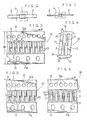
- Figure 1 is a side view showing a diode as an example of semiconductor devices to be produced by using the present invention;
- Figure 2 is a plan view showing the same diode;
- Figure 3 is a plan view showing a leadframe according to the present invention;
- Figure 4 is an enlarged fragmentary plan view showing a principal portion of the leadframe shown in Figure 3;
- Figure 5 is a plan view similar to Figure 3 but showing the leadframe after a first stage of chip bonding;
- Figure 6 is a plan view also similar to Figure 3 but showing the leadframe after final stage of chip bonding;
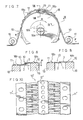
- Figure 7 is a front view showing a differential overlapping mechanism according to the present invention;
- Figure 8 is a sectional view taken on lines VIII-VIII in Figure 7;
- Figure 9 is a sectional view taken on lines IX-IX in Figure 7;
- Figure 10 is a plan view showing another leadframe according to the present invention;
- Figure 11 is a front view showing another differential overlapping mechanism according to the present invention;
- Figure 12 is a sectional view taken on lines XII-XII in Figure 11;
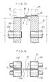
- Figure 13 is a sectional view taken on lines XIII-XIII in Figure 11;
- Figure 14 is a sectional view taken on lines XIV-XIV in Figure 11;
- Figures 15 to 17 are plan views showing the successive stages of a prior art method for manufacturing semiconductor devices; and
- Figure 18 is a plan view showing another prior art method of manufacturing semiconductor devices.
- Referring now to Figures 1 and 2, there is shown a semiconductor device which can be advantageously manufactured from a leadframe according to the present invention. The semiconductor device is illustrated as being in the form of a diode which comprises a semiconductor chip 1 held in conduction with a pair of
external leads - The leadframe embodying the present invention is illustrated in Figures 3 and 4. This leadframe, which is generally designated by
reference numeral 10, includes a pair oflongitudinal bands segments 13. The leadframe may be formed from a metallic plate to have a suitable width W and a substantially continuous length. - One longitudinal band 11 (hereafter referred to as "first band") is integrally formed with
leads 2 respectively arranged between the connectingsegments 13. The other longitudinal band 12 (hereafter referred to as "second band") is also formed withintegral leads 3 in corresponding relation to theleads 2 of the first band to provide lead pairs arranged within the respective spaces between the connecting segments. Each pair ofleads - The connecting
segments 13 are spaced from each other longitudinally of the leadframe at a suitable pitch P. According to the preferred embodiment shown in Figures 3 and 4, each connecting segment is inclined relative to the transverse direction of theleadframe 10, and has a pair ofneck portions longitudinal bands - For manufacture of semiconductor devices, the
leadframe 10 is transferred longitudinally thereof, as indicated by an arrow F in Figure 5. During such transfer, semiconductor chips 1 are bonded onto the tips of the respective leads 2 of the firstlongitudinal band 11. Upon subsequent transfer, the leadframe is passed through a differential overlapping mechanism to be described below, whereby each pair ofleads - As shown in Figures 7 to 9, the differential overlapping mechanism, which is arranged between a pair of
guide rollers leadframe 10, comprises a diametricallylarger feed wheel 18 and a diametricallysmaller feed wheel 19. Thelarger feed wheel 18, which is drivingly rotated on ashaft 18a, comes in feeding contact with the firstlongitudinal band 11 of the leadframe. Thesmaller feed wheel 19, which is drivingly rotated on ashaft 19a, comes in feeding contact with the secondlongitudinal band 12 of the leadframe, and has an outer circumference located partially outside and above the outer circumference of the larger feed wheel by a suitable amount H. The twowheels - The outer circumference of the
larger feed wheel 18 is provided with equiangularly spaced engagingprojections 18b for successive engagement with correspondingly spacedindexing holes 11a (see Figure 5) of the firstlongitudinal band 11. Similarly, the outer circumference of thesmaller wheel 19 is provided with equiangularly spaced engagingprojections 19b for successive engagement with correspondingly spacedindexing holes 12a (see Figure 5) of the secondlongitudinal band 12. In this way, theleadframe 10 passes through the differential overlapping mechanism without slippage. Alternatively, the twowheels - As illustrated in Figure 7, the
larger feed wheel 18 comes into feeding contact with the firstlongitudinal band 11 of theleadframe 10 along a larger diameter arc, whereas thesmaller feed wheel 19 comes into feeding contact with the secondlongitudinal band 12 of the leadframe along a smaller diameter arc. Both ends of the larger diameter arc are located substantially at the same positions as those of the smaller diameter arc. However, since the smaller diameter arc is displaced radially outwardly of the larger diameter arc by the amount H, the former is larger in length than the latter. Thus, when the two diametricallydifferent feed wheels lead 2 of the firstlongitudinal band 11 catches up thecorresponding lead 3 of the secondlongitudinal band 12 upon complete passage over the respective feed wheels. - Further, the positional deviation H between the respective contact arcs of the two
feed wheels lead 2 of the firstlongitudinal band 11 of theleadframe 10 displaces to a position under thecorresponding lead 3 of the secondlongitudinal band 12 during passage of the leadframe through the feed wheels, as best illustrated in Figure 8. Thus, combined with the longitudinal deviation described above, thelead 2 of the firstlongitudinal band 11 overlaps thecorresponding lead 3 of the secondlongitudinal band 12 after complete passage over the feed wheels, as shown in Figures 6 and 9. In this way, each semiconductor chip 1 bonded in advance to thelead 2 may be bonded to the other (couterpart) lead 3 as a result of processing within the differential overlapping mechanism. - To sum up, the differential overlapping mechanism has two important functions. First, this mechanism causes the first
longitudinal band 11 to slightly advance relative to the secondlongitudinal band 12 longitudinally of theleadframe 10. Second, the overlapping mechanism provides a level difference between the twolongitudinal bands leads longitudinal bands leadframe 10 through the overlapping mechanism but not before and after it because the twofeed wheels - Obviously, each connecting
segment 13 is deformed when the twolongitudinal bands leadframe 10. Thenarrower neck portions 14, 15 (figure 4) of the connectingsegment 13 provide positions for stress concentration to ensure that the segment is permanently deformed at these positions to prevent subsequent spring-back phenomenon of the leadframe. Moreover, the connectingsegment 13 remains substantially straight as a whole even after such deformation. - Further, each connecting
segment 13 is initially inclined relative to the transverse direction of theleadframe 10, as already described. However, when the twolongitudinal bands segments 13 become substantially rectangular to accommodate the respective molded resin bodies 4 which are subsequently formed within these spaces to become also rectangular. According to this arrangement, the pitch P (see Figure 3) may be made as small as possible to increase the number of semiconductor devices to be produced per unit length of theleadframe 10. - In the last stage of production, each semiconductor device thus formed is separated from the
leadframe 10 to provide the final product shown in Figures 1 and 2. - The present invention is not limited to the
particular leadframe 10 shown in Figures 3 to 6, wherein the twolongitudinal bands - Figure 10 shows one example of such modifications. Specifically, the modified
leadframe 10′ has a centrallongitudinal band 12′ (second longitudinal band) on both sides of which are disposed a pair of sidelongitudinal bands 11′ (first longitudinal bands) to enable successive production of semiconductor devices in two rows, thereby doubling productivity. As readily understood, a differential overlapping mechanism suitable for such a leadframe may comprise a central smaller feed wheel for feeding contact with the centrallongitudinal band 12′, and a pair of larger feed wheels arranged on both sides of the central wheel to come into feeding contact with the sidelongitudinal bands 11′. - Figures 11 to 14 show a modified differential overlapping mechanism according to the present invention. As shown, the modified overlapping mechanism, which is arranged between a pair of
guide rollers leadframe 10, comprises asmaller feed wheel 20 having a diameter d (Figure 13), and alarger feed wheel 21 having a larger diameter D. Thesmaller feed wheel 20 drivingly rotated on ashaft 20a comes in feeding contact with the firstlongitudinal band 11 of the leadframe. Thelarger feed wheel 21, which is drivingly rotated on ashaft 21a coaxial with theother shaft 20a, comes in feeding contact with the secondlongitudinal band 12. Thesmaller wheel 20 is rotated at a higher rotational speed than thelarger wheel 21, so that these two wheels have the same circumferential speed. - A first
nipping roller mechanism 22 is disposed between theupstream guide roller 16 and thefeed rollers nipping roller mechanism 23 is arranged between thedownstream guide roller 17 and the feed rollers. - As shown in Figure 12, the first
nipping roller mechanism 22 includes a pair of nippingrollers longitudinal band 11 of theleadframe 10. The first nipping roller mechanism further includes another pair of nippingrollers longitudinal band 12. - As shown in Figure 14, the second
nipping roller mechanism 23 includes a pair of nippingrollers longitudinal band 11 of theleadframe 10. The second nipping roller mechanism further incorporates another pair of nippingrollers longitudinal band 12. - With the arrangement described above, the
leadframe 10 is transferred longitudinally thereof by the driving rotation of the twofeed wheels - When the
leadframe 10 passes through the firstnipping roller mechanism 22, the twolongitudinal bands rollers 22a-22d, as already described. As a result, the twolongitudinal bands leadframe 10 by an amount H, as shown in Figure 12. This deviation H substantially corresponds to the difference in radius between the twofeed wheels rollers - As shown in Figure 11, the two diametrically
different feed wheels longitudinal bands leadframe 10 over substantially the same angle ϑ, so that the contact arc of thelarger feed wheel 21 is longer than that of thesmaller feed wheel 20 because of the diametrical difference between the two wheels. However, since the two feed wheels are rotated to have the same circumferential speed, the firstlongitudinal band 11 is advanced relative to the secondlongitudinal band 12 longitudinally of theleadframe 10 upon passage over the respective feed wheels. - When the
leadframe 10 passes through the secondnipping roller mechanism 23, the twolongitudinal bands lead 2 of the firstlongitudinal band 11 is overlapped with thecorresponding lead 3 of the secondlongitudinal band 12 with the semiconductor chip 1 interposed therebetween, as shown in Figure 14. - According the embodiment illustrated in Figures 11 to 14, the degree of relative longitudinal displacement between the two
longitudinal bands leadframe 10 may be adjusted by changing the diametrical difference between the twofeed wheels feed wheels roller mechanisms - In order to prevent slippage between the
leadframe 10 and thefeed wheels longitudinal bands - In view of such a problem, the differential overlapping mechanism shown in Figure 11 further incorporates a first pressing feed mechanism to cooperate with the
smaller feed wheel 20, and a second pressing feed mechanism to cooperate with thelarger feed wheel 21, as indicated in phantom lines. More specifically, the first pressing feed mechanism comprises a first set ofpulleys 24a-24d for guiding a firstendless belt 25 in pressing contact with the firstlongitudinal band 11 of theleadframe 10. Similarly, the second pressing feed mechanism comprises a second set ofpulleys 26a-26d for guiding a secondendless belt 27 in pressing contact with the secondlongitudinal band 12. - One
pulley 24a of the first pulley set and onepulley 26a of the second pulley set are used as drive pulleys which have the same diameter and are rotated at the same rotational speed. In this way, the twoendless belts feed wheels - According to the feeding arrangement shown in Figure 11, each
longitudinal band leadframe 10 is sandwiched between the correspondingendless belt feed wheel different feed wheels - The present invention being thus described, it is obvious that the same may be varied in many other ways. For instance, semiconductor chips 1 may be first bonded to the
leads 3 of the secondlongitudinal band 12 of theleadframe 10, whereafter the firstlongitudinal band 11 is raised and longitudinally advanced relative to the second longitudinal band to overlap theleads 2 of thefirst band 11 onto the counterpart leads 3 from above. Further, it is also possible to first bond the semiconductor chips 1 to the underside of theleads 3, whereafter thefirst band 11 is lowered and longitudinally advanced relative to thesecond band 12 to overlap theleads 2 onto the counterpart leads 3 from below. Such variations are not to be regarded as a departure from the spirit and scope of the present invention, and all such modifications as would be obvious to those skilled in the art are intended to be included in the scope of the following claims.
Claims (19)
causing said two bands (11, 11′, 12, 12′) to displace away from each other perpendicularly to a plane containing said leadframe (10, 10′);
causing said two bands to move relative to each other longitudinally of said leadframe so that each lead (2) of said first group assumes substantially the same longitudinal position as a corresponding lead (3) of said second group; and
causing said two bands to displace toward each other perpendicularly to said plane so that a semiconductor chip (1) on said each lead of said first group comes into contact with said corresponding lead of said second group for bonding.
a first feed wheel (18, 20) arranged in a path of transfer of said leadframe (10, 10′) and driven into rotation to have a specified circumferential speed, said first feed wheel having an outer circumference which provides a contact arc for coming into feeding contact with said one band (11, 11′); and
a second feed wheel (19, 21) arranged in side-by-side relation to said first feed wheel and driven into rotation to have the same circumferential speed as said first feed wheel, said second feed wheel having an outer circumference which provides a contact arc for coming into contact with said other longitudinal band (12, 12′), said contact arc of said second feed wheel being longer than said contact arc of said first feed wheel and positioned radially outwardly thereof.
Applications Claiming Priority (4)
| Application Number | Priority Date | Filing Date | Title |
|---|---|---|---|
| JP63184283A JPH0636422B2 (en) | 1988-07-22 | 1988-07-22 | Semiconductor device manufacturing method, lead frame used in the manufacturing method, and displacement device used in the manufacturing method |
| JP184283/88 | 1988-07-22 | ||
| JP106471/89 | 1989-04-25 | ||
| JP1106471A JPH0671015B2 (en) | 1989-04-25 | 1989-04-25 | Lead frame offset stacking device for semiconductor component manufacturing |
Publications (3)
| Publication Number | Publication Date |
|---|---|
| EP0351749A2 true EP0351749A2 (en) | 1990-01-24 |
| EP0351749A3 EP0351749A3 (en) | 1991-04-17 |
| EP0351749B1 EP0351749B1 (en) | 1996-01-17 |
Family
ID=26446590
Family Applications (1)
| Application Number | Title | Priority Date | Filing Date |
|---|---|---|---|
| EP89113056A Expired - Lifetime EP0351749B1 (en) | 1988-07-22 | 1989-07-17 | Method of manufacturing semiconductor devices, and leadframe and differential overlapping apparatus therefor |
Country Status (5)
| Country | Link |
|---|---|
| US (2) | US5038453A (en) |
| EP (1) | EP0351749B1 (en) |
| KR (1) | KR970006724B1 (en) |
| DE (1) | DE68925442T2 (en) |
| MY (2) | MY105015A (en) |
Cited By (1)
| Publication number | Priority date | Publication date | Assignee | Title |
|---|---|---|---|---|
| EP1121603A4 (en) * | 1998-10-15 | 2007-10-24 | Handy And Harman | METHOD AND SYSTEM FOR MANUFACTURING LAMP TILES |
Families Citing this family (44)
| Publication number | Priority date | Publication date | Assignee | Title |
|---|---|---|---|---|
| US5332405A (en) * | 1992-09-01 | 1994-07-26 | Golomb Mark S | Apparatus for manufacturing semiconductor lead frames in a circular path |
| US5506174A (en) * | 1994-07-12 | 1996-04-09 | General Instrument Corp. | Automated assembly of semiconductor devices using a pair of lead frames |
| US5821611A (en) * | 1994-11-07 | 1998-10-13 | Rohm Co. Ltd. | Semiconductor device and process and leadframe for making the same |
| MY122101A (en) | 1997-03-28 | 2006-03-31 | Rohm Co Ltd | Lead frame and semiconductor device made by using it |
| US6669749B1 (en) | 2000-02-02 | 2003-12-30 | 3M Innovative Properties Company | Fused abrasive particles, abrasive articles, and methods of making and using the same |
| US6451077B1 (en) | 2000-02-02 | 2002-09-17 | 3M Innovative Properties Company | Fused abrasive particles, abrasive articles, and methods of making and using the same |
| WO2001056950A1 (en) | 2000-02-02 | 2001-08-09 | 3M Innovative Properties Company | Fused abrasive particles, abrasive articles, and methods of making and using the same |
| US6607570B1 (en) | 2000-02-02 | 2003-08-19 | 3M Innovative Properties Company | Fused Al2O3-rare earth oxide eutectic abrasive particles, abrasive articles, and methods of making and using the same |
| US6596041B2 (en) | 2000-02-02 | 2003-07-22 | 3M Innovative Properties Company | Fused AL2O3-MgO-rare earth oxide eutectic abrasive particles, abrasive articles, and methods of making and using the same |
| US6592640B1 (en) | 2000-02-02 | 2003-07-15 | 3M Innovative Properties Company | Fused Al2O3-Y2O3 eutectic abrasive particles, abrasive articles, and methods of making and using the same |
| US6583080B1 (en) | 2000-07-19 | 2003-06-24 | 3M Innovative Properties Company | Fused aluminum oxycarbide/nitride-Al2O3·rare earth oxide eutectic materials |
| US6582488B1 (en) | 2000-07-19 | 2003-06-24 | 3M Innovative Properties Company | Fused Al2O3-rare earth oxide-ZrO2 eutectic materials |
| US6666750B1 (en) | 2000-07-19 | 2003-12-23 | 3M Innovative Properties Company | Fused AL2O3-rare earth oxide-ZrO2 eutectic abrasive particles, abrasive articles, and methods of making and using the same |
| US6458731B1 (en) | 2000-07-19 | 2002-10-01 | 3M Innovative Properties Company | Fused aluminum oxycarbide/nitride-AL2O3.Y2O3 eutectic materials |
| US6589305B1 (en) | 2000-07-19 | 2003-07-08 | 3M Innovative Properties Company | Fused aluminum oxycarbide/nitride-Al2O3 • rare earth oxide eutectic abrasive particles, abrasive articles, and methods of making and using the same |
| US6454822B1 (en) | 2000-07-19 | 2002-09-24 | 3M Innovative Properties Company | Fused aluminum oxycarbide/nitride-Al2O3·Y2O3 eutectic abrasive particles, abrasive articles, and methods of making and using the same |
| EP1303464B1 (en) | 2000-07-19 | 2006-06-28 | 3M Innovative Properties Company | Fused aluminum oxycarbide/nitride-aluminum rare earth oxide eutectic materials, abrasive particles, abrasive articles and methods of making and using the same |
| JP2004504448A (en) | 2000-07-19 | 2004-02-12 | スリーエム イノベイティブ プロパティズ カンパニー | Molten Al2O3-rare earth oxide-ZrO2 eutectic material, abrasive particles, abrasive article, and methods of making and using them |
| US7384438B1 (en) | 2000-07-19 | 2008-06-10 | 3M Innovative Properties Company | Fused Al2O3-Y2O3-ZrO2 eutectic abrasive particles, abrasive articles, and methods of making and using the same |
| AU2002213054A1 (en) * | 2000-10-06 | 2002-04-15 | 3M Innovative Properties Company | Ceramic aggregate particles |
| DE60141700D1 (en) | 2000-10-16 | 2010-05-12 | 3M Innovative Properties Co | ATTEILCHEN |
| MXPA03003290A (en) | 2000-10-16 | 2004-05-04 | 3M Innovative Properties Co | Method of making an agglomerate particles. |
| US6521004B1 (en) | 2000-10-16 | 2003-02-18 | 3M Innovative Properties Company | Method of making an abrasive agglomerate particle |
| US6551366B1 (en) | 2000-11-10 | 2003-04-22 | 3M Innovative Properties Company | Spray drying methods of making agglomerate abrasive grains and abrasive articles |
| KR100885329B1 (en) | 2001-08-02 | 2009-02-26 | 쓰리엠 이노베이티브 프로퍼티즈 컴파니 | Al₂O₃-rare earth oxide-ZrO₂ / HfO₂ materials, and preparation and use thereof |
| CN101417860B (en) | 2001-08-02 | 2012-01-18 | 3M创新有限公司 | Method of making articles from glass and glass ceramic articles so produced |
| KR100885328B1 (en) * | 2001-08-02 | 2009-02-26 | 쓰리엠 이노베이티브 프로퍼티즈 컴파니 | Alumina-Yttrium Oxide-Zirconium Oxide / Hafnium Oxide Materials, and Methods for Making and Using the Same |
| CN100453486C (en) | 2001-08-02 | 2009-01-21 | 3M创新有限公司 | Abrasive particles and methods of making and using the same |
| US7625509B2 (en) | 2001-08-02 | 2009-12-01 | 3M Innovative Properties Company | Method of making ceramic articles |
| AU2002321872A1 (en) | 2001-08-02 | 2003-02-17 | 3M Innovative Properties Company | Abrasive particles, and methods of making and using the same |
| US6572666B1 (en) | 2001-09-28 | 2003-06-03 | 3M Innovative Properties Company | Abrasive articles and methods of making the same |
| US6803255B2 (en) * | 2002-07-31 | 2004-10-12 | Delphi Technologies, Inc. | Dual gauge lead frame |
| US7179526B2 (en) | 2002-08-02 | 2007-02-20 | 3M Innovative Properties Company | Plasma spraying |
| US8056370B2 (en) | 2002-08-02 | 2011-11-15 | 3M Innovative Properties Company | Method of making amorphous and ceramics via melt spinning |
| US7175786B2 (en) | 2003-02-05 | 2007-02-13 | 3M Innovative Properties Co. | Methods of making Al2O3-SiO2 ceramics |
| US7811496B2 (en) | 2003-02-05 | 2010-10-12 | 3M Innovative Properties Company | Methods of making ceramic particles |
| US7258707B2 (en) | 2003-02-05 | 2007-08-21 | 3M Innovative Properties Company | AI2O3-La2O3-Y2O3-MgO ceramics, and methods of making the same |
| US7197896B2 (en) | 2003-09-05 | 2007-04-03 | 3M Innovative Properties Company | Methods of making Al2O3-SiO2 ceramics |
| US7141522B2 (en) | 2003-09-18 | 2006-11-28 | 3M Innovative Properties Company | Ceramics comprising Al2O3, Y2O3, ZrO2 and/or HfO2, and Nb2O5 and/or Ta2O5 and methods of making the same |
| US7297171B2 (en) | 2003-09-18 | 2007-11-20 | 3M Innovative Properties Company | Methods of making ceramics comprising Al2O3, REO, ZrO2 and/or HfO2 and Nb205 and/or Ta2O5 |
| US7141523B2 (en) | 2003-09-18 | 2006-11-28 | 3M Innovative Properties Company | Ceramics comprising Al2O3, REO, ZrO2 and/or HfO2, and Nb2O5 and/or Ta2O5 and methods of making the same |
| US7399330B2 (en) * | 2005-10-18 | 2008-07-15 | 3M Innovative Properties Company | Agglomerate abrasive grains and methods of making the same |
| US7281970B2 (en) | 2005-12-30 | 2007-10-16 | 3M Innovative Properties Company | Composite articles and methods of making the same |
| US7598188B2 (en) | 2005-12-30 | 2009-10-06 | 3M Innovative Properties Company | Ceramic materials and methods of making and using the same |
Family Cites Families (19)
| Publication number | Priority date | Publication date | Assignee | Title |
|---|---|---|---|---|
| NL283249A (en) * | 1961-09-19 | 1900-01-01 | ||
| DE1514822A1 (en) * | 1964-08-14 | 1969-06-26 | Telefunken Patent | Method for manufacturing a semiconductor device |
| US3430115A (en) * | 1966-08-31 | 1969-02-25 | Webb James E | Apparatus for ballasting high frequency transistors |
| US3577633A (en) * | 1966-12-02 | 1971-05-04 | Hitachi Ltd | Method of making a semiconductor device |
| DE2054677B2 (en) * | 1970-11-06 | 1977-12-22 | Semikron Gesellschaft für Gleichrichterbau und Elektronik mbH, 8500 Nürnberg | METHOD OF MANUFACTURING SEMI-CONDUCTOR RECTIFIER ARRANGEMENTS |
| US3698076A (en) * | 1970-08-03 | 1972-10-17 | Motorola Inc | Method of applying leads to an integrated circuit |
| CA915318A (en) * | 1971-04-27 | 1972-11-21 | Microsystems International Limited | Method and apparatus for manufacture of integrated circuit devices |
| US4079509A (en) * | 1972-01-29 | 1978-03-21 | Ferranti Limited | Method of manufacturing semi-conductor devices |
| US3839782A (en) * | 1972-03-15 | 1974-10-08 | M Lincoln | Method for using a lead frame for the manufacture of electric devices having semiconductor chips placed in a face-to-face relation |
| US3859718A (en) * | 1973-01-02 | 1975-01-14 | Texas Instruments Inc | Method and apparatus for the assembly of semiconductor devices |
| JPS5144385B2 (en) * | 1973-02-16 | 1976-11-27 | ||
| US4069924A (en) * | 1976-11-18 | 1978-01-24 | Western Electric Co., Inc. | Methods and apparatus for positioning an article laterally on a support |
| JPS5380187A (en) * | 1976-12-25 | 1978-07-15 | Fujitsu Ltd | Manufacture of semiconductor device |
| US4252864A (en) * | 1979-11-05 | 1981-02-24 | Amp Incorporated | Lead frame having integral terminal tabs |
| NL8001114A (en) * | 1980-02-25 | 1981-09-16 | Philips Nv | DEVICE FOR MOUNTING CONNECTION WIRELESS PLATE OR BLOCKED ELECTRONIC COMPONENTS ON A SUBSTRATE. |
| US4616250A (en) * | 1984-07-03 | 1986-10-07 | Motorola, Inc. | Contact assembly for small semiconductor device |
| JPS6235549A (en) * | 1985-08-08 | 1987-02-16 | Mitsubishi Electric Corp | Rectifier |
| JPH0636393B2 (en) * | 1987-04-15 | 1994-05-11 | 松下電器産業株式会社 | Electronic component manufacturing method |
| US4859632A (en) * | 1987-12-28 | 1989-08-22 | Siemens Corporate Research And Support, Inc. | Method for manufacturing the same |
-
1989
- 1989-07-11 US US07/377,969 patent/US5038453A/en not_active Expired - Lifetime
- 1989-07-12 MY MYPI89000956A patent/MY105015A/en unknown
- 1989-07-17 EP EP89113056A patent/EP0351749B1/en not_active Expired - Lifetime
- 1989-07-17 DE DE68925442T patent/DE68925442T2/en not_active Expired - Lifetime
- 1989-07-21 KR KR1019890010362A patent/KR970006724B1/en not_active Expired - Fee Related
-
1990
- 1990-12-11 US US07/625,536 patent/US5068206A/en not_active Expired - Lifetime
-
1994
- 1994-02-22 MY MYPI94000404A patent/MY112386A/en unknown
Cited By (1)
| Publication number | Priority date | Publication date | Assignee | Title |
|---|---|---|---|---|
| EP1121603A4 (en) * | 1998-10-15 | 2007-10-24 | Handy And Harman | METHOD AND SYSTEM FOR MANUFACTURING LAMP TILES |
Also Published As
| Publication number | Publication date |
|---|---|
| DE68925442T2 (en) | 1996-05-30 |
| DE68925442D1 (en) | 1996-02-29 |
| KR970006724B1 (en) | 1997-04-29 |
| EP0351749A3 (en) | 1991-04-17 |
| KR900002437A (en) | 1990-02-28 |
| US5038453A (en) | 1991-08-13 |
| US5068206A (en) | 1991-11-26 |
| EP0351749B1 (en) | 1996-01-17 |
| MY112386A (en) | 2001-06-30 |
| MY105015A (en) | 1994-07-30 |
Similar Documents
| Publication | Publication Date | Title |
|---|---|---|
| US5038453A (en) | Method of manufacturing semiconductor devices, and leadframe and differential overlapping apparatus therefor | |
| US5208481A (en) | Lead-frame for manufacturing semiconductor devices | |
| EP0056946B1 (en) | An arrangement for the feeding of objects | |
| US4573501A (en) | Apparatus for cutting and forming leads | |
| US5343072A (en) | Method and leadframe for making electronic components | |
| CA1152039A (en) | Carrier assembly apparatus | |
| US4429559A (en) | Strip processing apparatus | |
| CA1280774C (en) | Feed conveyor for machine for forming leads of electronic components | |
| US5158410A (en) | Belt and drive for conversion press | |
| TW201934450A (en) | Conveying method and device of carrier tape comprising a carrier tape transfer step, a carrier tape traction step, and a tension control step detecting a position of a gravity wheel arranged between first and second driving mechanisms | |
| CN214555373U (en) | Intelligent sorting machine and intelligent sorting system | |
| CN86106209A (en) | Multipack coupling, method and apparatus | |
| US5259911A (en) | Apparatus for automatically taping electronic components | |
| GB2126185A (en) | Means and method for conveying and orienting randomized circular product-carrying pucks | |
| EP0336063A2 (en) | Container conveying mechanism | |
| KR102621500B1 (en) | Device for banding products | |
| US4093480A (en) | Method for making electrical connectors | |
| JPH0671015B2 (en) | Lead frame offset stacking device for semiconductor component manufacturing | |
| US3844093A (en) | Apparatus for decapping bottles | |
| JPH0425162A (en) | Shift overlapping device for semiconductor component manufacturing lead frame | |
| JPH08337801A (en) | Fettling device | |
| JP3438780B2 (en) | Method and apparatus for forming protective coating film for diode element | |
| JPH089809Y2 (en) | Transporting mechanism of direction changing part in coin processing machine | |
| JP2000024789A (en) | Drive transmission mechanism of tubular roller table | |
| JPH10242186A (en) | Mold digating apparatus and method |
Legal Events
| Date | Code | Title | Description |
|---|---|---|---|
| PUAI | Public reference made under article 153(3) epc to a published international application that has entered the european phase |
Free format text: ORIGINAL CODE: 0009012 |
|
| AK | Designated contracting states |
Kind code of ref document: A2 Designated state(s): DE FR GB NL |
|
| PUAL | Search report despatched |
Free format text: ORIGINAL CODE: 0009013 |
|
| AK | Designated contracting states |
Kind code of ref document: A3 Designated state(s): DE FR GB NL |
|
| 17P | Request for examination filed |
Effective date: 19910716 |
|
| 17Q | First examination report despatched |
Effective date: 19930722 |
|
| GRAA | (expected) grant |
Free format text: ORIGINAL CODE: 0009210 |
|
| AK | Designated contracting states |
Kind code of ref document: B1 Designated state(s): DE FR GB NL |
|
| REF | Corresponds to: |
Ref document number: 68925442 Country of ref document: DE Date of ref document: 19960229 |
|
| ET | Fr: translation filed | ||
| PLBE | No opposition filed within time limit |
Free format text: ORIGINAL CODE: 0009261 |
|
| STAA | Information on the status of an ep patent application or granted ep patent |
Free format text: STATUS: NO OPPOSITION FILED WITHIN TIME LIMIT |
|
| 26N | No opposition filed | ||
| REG | Reference to a national code |
Ref country code: GB Ref legal event code: IF02 |
|
| PGFP | Annual fee paid to national office [announced via postgrant information from national office to epo] |
Ref country code: DE Payment date: 20080724 Year of fee payment: 20 |
|
| PGFP | Annual fee paid to national office [announced via postgrant information from national office to epo] |
Ref country code: FR Payment date: 20080718 Year of fee payment: 20 Ref country code: NL Payment date: 20080715 Year of fee payment: 20 |
|
| PGFP | Annual fee paid to national office [announced via postgrant information from national office to epo] |
Ref country code: GB Payment date: 20080723 Year of fee payment: 20 |
|
| REG | Reference to a national code |
Ref country code: GB Ref legal event code: PE20 Expiry date: 20090716 |
|
| NLV7 | Nl: ceased due to reaching the maximum lifetime of a patent |
Effective date: 20090717 |
|
| PG25 | Lapsed in a contracting state [announced via postgrant information from national office to epo] |
Ref country code: GB Free format text: LAPSE BECAUSE OF EXPIRATION OF PROTECTION Effective date: 20090716 Ref country code: NL Free format text: LAPSE BECAUSE OF EXPIRATION OF PROTECTION Effective date: 20090717 |