EP0349820B1 - Module et architecture de réseau pour l'émulation programmable des réseaux neuronaux artificiels numériques - Google Patents
Module et architecture de réseau pour l'émulation programmable des réseaux neuronaux artificiels numériques Download PDFInfo
- Publication number
- EP0349820B1 EP0349820B1 EP89111121A EP89111121A EP0349820B1 EP 0349820 B1 EP0349820 B1 EP 0349820B1 EP 89111121 A EP89111121 A EP 89111121A EP 89111121 A EP89111121 A EP 89111121A EP 0349820 B1 EP0349820 B1 EP 0349820B1
- Authority
- EP
- European Patent Office
- Prior art keywords
- neuron
- neurons
- inputs
- network
- discriminator
- Prior art date
- Legal status (The legal status is an assumption and is not a legal conclusion. Google has not performed a legal analysis and makes no representation as to the accuracy of the status listed.)
- Expired - Lifetime
Links
Images


Classifications
-
- G—PHYSICS
- G06—COMPUTING; CALCULATING OR COUNTING
- G06N—COMPUTING ARRANGEMENTS BASED ON SPECIFIC COMPUTATIONAL MODELS
- G06N3/00—Computing arrangements based on biological models
- G06N3/02—Neural networks
- G06N3/04—Architecture, e.g. interconnection topology
Definitions
- the present invention relates to a network construction Tern and a network architecture for programmable emulation large k ünst Anlagen n euronaler NETWORKS KNN with digital operation.
- KNN Artificial neural networks
- Such a KNN consists of a large number of nonlinear processor elements (neurons) which are networked with one another via variable "weight factors".
- a significant reduction in computing time and a much larger sample throughput can be obtained with hardware emulators.
- hardware simulators In contrast to hardware simulators, they contain an artificial neural network of small size, which can be used to emulate a larger network.
- the advantage of a digital implementation of a KNN is, in addition to a higher throughput, the greater freedom with which the user can select and set network-typical parameters (e.g. discriminator functions).
- neuro-emulators since the algorithm of a neural network cannot be executed faster with any architecture than with the neural one, and on the other hand, networks with only a few 100 neurons cannot be used reasonably because of their small memory capacity, so the design of digital emulators for artificial neural networks referred to as neuro-emulators), the following points must be considered in particular:
- the object of the present invention is to create a network architecture of the type mentioned at the outset for the construction of large digital neural networks, which allows small neuron units to be used which can be implemented using the technological possibilities currently available.
- a digital basic module is proposed according to claim 1.
- a corresponding network architecture is proposed in claim 5.
- a small neural network with m neurons and m2 multipliers is provided for the weighting.
- the chosen architecture allows a fast emulation of any network structure with all the above-mentioned non-linear transmission characteristics of the artificial neurons.
- the hardware architecture according to the invention makes it possible to set up large neural networks with smaller ones for which a hardware implementation is still possible.
- Several of these small networks can, for example, be combined into larger ones, or the algorithm (1) of a large network is scanned with the algorithm of a small network. The latter means emulating a large network using a smaller one.
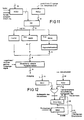
- Fig. 1 shows the architecture of the 4-neuron unit.
- a neuron consists of four multipliers, two adders, an accumulator, two multiplexers and a discriminator (binary, "linear ramp", sigmoidal and tanh characteristics are available).
- a multiplier is provided which, among other things, can distribute the characteristic of the sigmoidal function and thereby also support a Boltzmann distribution.
- the lines for threshold values and non-branching inputs can be saved if additional clocks are used. For example, if you put b1, b2 b3, b4 on the branching inputs and the weight inputs (w1000), (0w200), (00w30), (000w4) and replace b i or w i with 1 or ⁇ i in the next bar , w i b i + ⁇ i is calculated. This is followed, as described, by the weighting of the branching inputs. Overall, the computing time increases by 2 M / m cycles. In this way, 64 pads and four adders can be saved, see FIG. 3.
- FIG. 5 shows the local memory periphery of the "type 1" neuro emulator constructed with a single 4-neuron unit. It is designed for a network with a maximum of 100,000 inputs (limited by the bit width of the accumulator) and a maximum of 64 million weights (8 bits each). Since the product of the number of 8-bit inputs and the number of 8-bit outputs must remain ⁇ 64 ⁇ 106, a "fast" interface is also provided, via which the weights can be read in from the outside. The disadvantage is that the interface must be 128 x 20 Mbit / s fast. The local memory, however, allows a serial interface with a smaller bandwidth.
- the weights must either be transferred via a very wide and fast interface or by reading out a local memory. With a cycle time of just 50 ns, a data rate of 20 Mbit / s results for each pin (bit) and bit line (bit-line).
- the basic module described is well suited for embedding in a linear systolic arrangement, see T. Noll: Systolic cell fields. ITG technical reports, vol. 98, "Großintegration", pp. 203 - 207, Baden-Baden, 1987 and U. Ramacher: "A self testing WSI matrix-matrix multiplier", Proc. of the IFIP Workshop on Wafer Scale Integration, Brunel, UK, Sept. 1987. If L m neuron units are connected in series, see FIG. 6, the input vectors a1 ... aN no longer have to be M / m times, but only repeated M / (Lm) times. In this way, large neuro-emulators can be built with m * L neurons, which in turn can very quickly emulate even larger neural networks.
- the output vectors y l ... y m are read into the first output register of the first m-neuron unit via the multiplexer.
- the second unit sends its output vectors y m + 1 ... y 2m to its first output register via the multiplexer.
- y l ... y m are in the second output register of the first m-neuron unit.
- the L-link chain first outputs the output vectors y 4L - 3 ... y 4L and last y1 ... y4. Since M ⁇ 4L applies in general, the input vectors must be sent M / 4L times in succession into the arrangement until all output vectors y 1 ... y M are available.
- the throughput is determined by the first summand in (9).
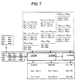
- the "Type 2" neuro emulator consists of 250 4-neuron units. NM / 250 weights are required per 4-neuron unit. If 128 x 128 kbit per unit is provided as local memory, 5.24 x 10⁸ connections can be realized. Since the accumulator of the 4-neuron unit ensures the desired 8-bit accuracy of the output vectors for a maximum of 100,000 input vectors, the interfaces shown in FIG. 8 and the memory periphery also shown at this point result.
- the "Type 2" neuro emulator manages with the same number of pins for the data lines as the "Type 1" neuro emulator. At the same time, the "Type 2" neuro emulator comes with significantly improved performance features compared to the "Type 1" neuro emulator, see below.
- the 32 32 kbit memories are provided twice in order to be able to carry out read / write operations simultaneously.
- the advantage of the local memory for the weights, as mentioned, is that the 250 weight memories can be loaded serially. This requires a multiple of the computing time and is not critical since the weights in the detection phase do not change over long sequences of input vectors.
- the weights W ij change by a ⁇ (W ij ) after each set of N input vectors, on the other hand care must be taken when developing the architecture of the basic module for the learning phase that these changes ⁇ (W ij ) are internally offset against the weights W ij and accumulated over the duration of the learning phase.
- the learned weights W ' ij can then be loaded into the weight memory.
- the neuro emulator "Type 2" consists of 1000 neurons instead of 4, the above considerations apply.
- the bidirectionality of the branching inputs of the "Type 1" emulator (FIG. 1) and of the "Type 2" emulator can be used for an advantageous realization of a possibly necessary iteration with the "Type 2" emulator. It is advantageous, since the output vectors of the systolic arrangement appear at the other end of the arrangement than the input vectors, to be able to feed in the complete set of the M output vectors at this end of the arrangement and to send them through the arrangement in the opposite direction. The data flow on the branching inputs would therefore be after each iteration change direction. This can be achieved with bidirectional drivers and registers.
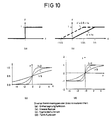
- the task of the discriminator unit is to implement the non-linear transfer function of the neuron. In order to achieve maximum flexibility, this unit contains all the transmission characteristics that are important for neural networks.
- the input signal z of the discriminator (output of the accumulator AKK in Fig. 1) is coded with 32 bits in a two's complement representation, the least significant bit being 2 ⁇ 14.
- the following non-linear discriminator functions are implemented in the discriminator unit:
- the output signal y is always equal to or greater than zero.
- the value range (0, 1) can be mapped to (-1, 1).
- the sigmoidal function and the hyperbolic function can be changed can be changed (see Fig. 10b, c, d).
- the value range of ⁇ is chosen so that the curves can be both steeper ( ⁇ > 1) and flatter ( ⁇ ⁇ 1) compared to an evaluation with 1.
- the value range of the weight factors can also be changed with the aid of the parameter.
- the number range therefore extends from 0 to + 32768 - 2 ⁇ 16.
- the block diagram of the discriminator unit is shown in Fig. 11.
- the constant ⁇ and the numerical value of z are stored in registers REG1 and REG2.
- REG1 is read out serially, and the multiplication with z is carried out in the subsequent serial multiplication unit.
- the number format is then reduced to the required word width with the aid of saturation multiplexers. In the case of the binary decision maker, only the sign bit needs to be forwarded.
- the output signal of the saturation multiplexer is passed on unchanged, while with the sigmoidal function and the TANH function, a line approximation is carried out in a further unit.
- the linear number transformation is carried out for the generation of negative output number values.
- the signal z is multiplied by the parameter ⁇ in a serial multiplier unit.
- the numerical value stored in the register is read out serially starting with the least significant bit and fed to the multiplication unit (see FIG. 12).
- the provided accumulator register REG3 must be reset (reset signal in FIG. 12).
- the first term, ⁇ 0 z is then stored in the accumulator register REG3. The return to the adder takes place via a hard-wired "right shift" by one position, whereby the sign is doubled (arithmetic shift, multiplication of the partial sum by 2 ⁇ 1).
- the output signal of the discriminator should, however, be limited to 8 bit word width. In the case of the binary decision maker, it is ultimately sufficient to query the sign, but in the ramp function the word width must be limited to 8 bits using a saturation characteristic.
- the error should be less than an LSB, i.e. less than 2 ⁇ 7.
- An accuracy estimate shows that the number range from z 'can be limited to the interval (-8.8) and that the significance of the least significant bit must not be greater than 2 ⁇ 5. It follows that at least 9 bits are required for the representation of numbers z '. Accordingly, a second saturation multiplexer is required, the saturation characteristics of given is.
- the size z s ' denotes the output signal of this saturation multiplexer.
- FIG. 13 A joint implementation of the two functions is shown in FIG. 13. Since the LSB of z 'has the value 2 ⁇ 7, the seven least significant bits must be selected when using the ramp function. If z ' ⁇ 1 - 2 ⁇ 7, that is, if the sign bit is 0 and at least one of the remaining 25 leading bits is 1, all output bits with the exception of the sign should be set to 1. This is done with the help of multiplexers MUX (1) to MUX (7). The inputs shown on the left with the exception of MUX (3) are in this case set to 1 by the inverted sign bit, while the corresponding input of MUX (3) is set to 1 by the provided PLA (programmable logic arrangement). The switching of the multiplexers is also controlled by this PLA. The same applies to z ′ ⁇ 0, ie if the sign bit is 1 and at least one of the remaining 25 leading bits is 0. In this case, all output bits should be set to 0.
- the MSB and the remaining 22 bits have to be examined to determine whether the value range has been exceeded.
- the output signal is now formed using the multiplexers MUX (3) to MUX (10), the LSB always being 1 when saturated (see Eq. (14)), while the remaining bits are formed in the same way as before.
- y 0.5 + sign (z ′) ⁇ m1 ⁇
- y 0.5 + sign (z ′) ⁇ ⁇ m1 ⁇ z1 ′ + m2 (
- y 0.5 + sign (z ′) ⁇ ⁇ m1 ⁇ z1 ′ + m2 (z2 ′ - z1 ′) + ... m i-1 (Z.
- the least significant bits up to and including position 2 L-1 just contain the term (
- the numerical values of z i and m i can be stored in a ROM which is addressed directly by these higher-order bits.
- - (k - 1) 2 L ) and the addition to C i can be carried out serially. Depending on the sign of z ′, the result is added to 0.5 or subtracted from it.
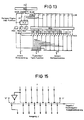
- FIG. 14 A circuit implementation is shown in FIG. 14.
- the number z ′ encoded with 9 bits in two's complement is converted into a sign-amount representation. For this the amount of z 'is first formed, while the sign bit remains unchanged. The amount is stored in the 8-bit wide register REG2.
- the three high-order bits of this register (segment identifier) are required for calling C i and m i , C i is loaded into an accumulator register REG4, m i in REG3 via the multiplexer MUX2.
- the least significant 5 bits of register REG2 are then read out serially, starting with the LSB. With the help of the AND gate, a partial product is calculated in each cycle and added to the contents of the accumulator.
- the circuit implementation (Fig. 15) essentially consists of a multiplexer.
- the multiplication by 2 is carried out very simply by a hard-wired left shift and the addition of 2 ⁇ 7 by a 1 at the least significant multiplexer input. An inverting of the most significant bit is only required for the addition of -1.
Landscapes
- Engineering & Computer Science (AREA)
- Theoretical Computer Science (AREA)
- Physics & Mathematics (AREA)
- Data Mining & Analysis (AREA)
- General Health & Medical Sciences (AREA)
- Biomedical Technology (AREA)
- Biophysics (AREA)
- Computational Linguistics (AREA)
- Life Sciences & Earth Sciences (AREA)
- Evolutionary Computation (AREA)
- Artificial Intelligence (AREA)
- Molecular Biology (AREA)
- Computing Systems (AREA)
- General Engineering & Computer Science (AREA)
- General Physics & Mathematics (AREA)
- Mathematical Physics (AREA)
- Software Systems (AREA)
- Health & Medical Sciences (AREA)
- Complex Calculations (AREA)
Claims (10)
- Module de base numérique comportant m neurones pour l'établissement de réseaux neuroniques artificiels comportant N entrées et M sorties, et dans lequel- chaque neurone est constitué par une colonne contenant m multiplicateurs (MUL1 à MUL4), deux additionneurs (AD2), un accumulateur (AKK), deux multiplexeurs (MUX) et un discriminateur,- des courbes caractéristiques de tous les discriminateurs peuvent être modifiées au choix, par modification des contenus de registres correspondants (REG),- m entrées de ramification (E1...E4) sont prévues, chacune d'elles étant raccordée côté entrée respectivement à m multiplicateurs, à savoir respectivement à un multiplicateur de chacun des m neurones,- m entrées non ramificatrices (wibi) sont prévues, chacune d'elles étant raccordée, côté entrée, à un second des deux additionneurs respectivement de l'un des m neurones,- chacun de ces multiplicateurs multiplie son signal d'entrée (E1...E4) par l'un de m x m coefficients de pondération,- le premier des deux additionneurs de chaque neurone additionne les signaux de sortie des multiplicateurs de ce neurone,- le second additionneur de chaque neurone ajoute l'une des m valeurs de seuil à respectivement l'une des m entrées non ramificatrices, et- les résultats du premier additionneur sont envoyés, par l'intermédiaire de l'accumulateur de chaque neurone, au discriminateur du neurone considéré, qui détermine la valeur de sortie, qui correspond à ce neurone, des m valeurs de sortie du module de base,- la sortie du résultat du commutateur est envoyée, par l'interémdiaire du premier multiplexeur (MUX), soit au discriminateur, soit au second multiplexeur, et- soit le signal de sortie du second additionneur, soit le signal de sortie du premier multiplexeur peut être envoyé à une seconde entrée de l'accumulateur, à l'aide du second multiplexeur, pour la formation d'une voie d'accumulation.
- Module de base suivant la revendication 1, dont le discriminateur possède une courbe caractéristique, dont la caractéristique est au choix une fonction de saut (figure 10a) ou une fonction en rampe linéaire (figure 10b), une fonction sigmoïdale (figure 10c) ou une fonction tangente hyperbolique (tanh) (figure 10d).
- Module de base suivant l'une des revendications précédentes, qui comporte des registres (REG1,REG2) pour la mémorisation de données et en aval desquels est branchée une unité de multiplication série (SM), dont les sorties sont reliées, pour limiter le format des chiffres du résultat de la multiplication, aux entrées de multiplexeurs de saturation (SMUX) prévus à cet effet.
- Module de base suivant l'une des revendications précédentes, avec m = 4.
- Architecture de réseau pour l'émulation de réseaux neuroniques artificiels comportant N entrées et M sorties, dans laquelle une multiplicité formée de L modules de base numérique selon l'une des revendications précédentes sont reliés entre eux selon un mode systolique.
- Architecture de réseau suivant la revendication 5, dans laquelle les signaux d'entrée de modules de base suivants sont retardés par rapport aux signaux d'entrée de modules de base précédents.
- Architecture de réseau suivant l'une des revendications précédentes, caractérisée par le fait que ce qu'on appelle un réseau Instar est formé au moyen des neurones.
- Architecture de réseau suivant l'une revendications 1 à 6, caractérisée par le fait qu'un réseau dit Outstar est formé au moyen des neurones.
- Architecture de réseau suivant l'une des revendications 1 à 6, caractérisée par le fait que ce qu'on appelle un Feedforward-Multilayer-Perceptron est formé au moyen des neurones.
- Architecture de réseau suivant l'une des revendications 1 à 6, caractérisée par le fait que ce qu'on appelle un réseau Hopfield est formé au moyen des neurones.
Applications Claiming Priority (2)
| Application Number | Priority Date | Filing Date | Title |
|---|---|---|---|
| DE3822758 | 1988-07-05 | ||
| DE3822758 | 1988-07-05 |
Publications (2)
| Publication Number | Publication Date |
|---|---|
| EP0349820A1 EP0349820A1 (fr) | 1990-01-10 |
| EP0349820B1 true EP0349820B1 (fr) | 1995-04-19 |
Family
ID=6358016
Family Applications (1)
| Application Number | Title | Priority Date | Filing Date |
|---|---|---|---|
| EP89111121A Expired - Lifetime EP0349820B1 (fr) | 1988-07-05 | 1989-06-19 | Module et architecture de réseau pour l'émulation programmable des réseaux neuronaux artificiels numériques |
Country Status (4)
| Country | Link |
|---|---|
| US (1) | US5253330A (fr) |
| EP (1) | EP0349820B1 (fr) |
| JP (1) | JPH0258157A (fr) |
| DE (1) | DE58909182D1 (fr) |
Families Citing this family (24)
| Publication number | Priority date | Publication date | Assignee | Title |
|---|---|---|---|---|
| CA2035338C (fr) * | 1990-03-21 | 1995-07-25 | Bernhard Boser | Accroissement de la vitesse operationnelle des reseaux neuraux |
| US5065339A (en) * | 1990-05-22 | 1991-11-12 | International Business Machines Corporation | Orthogonal row-column neural processor |
| DE69130656T2 (de) | 1990-06-14 | 1999-06-17 | Canon Kk | Neuronale Netzwerke |
| JPH07113917B2 (ja) * | 1991-03-20 | 1995-12-06 | エイ・ティ・アンド・ティ・コーポレーション | ニューラル・ネットワーク及びその制御方法及びニューラル・ネットワーク用演算装置 |
| US5350953A (en) * | 1993-05-28 | 1994-09-27 | Swenson Richard M | Digitally weighted neuron for artificial neural network |
| US5473731A (en) * | 1993-07-20 | 1995-12-05 | Intel Corporation | Lattice based dynamic programming classification system |
| US5535148A (en) * | 1993-09-23 | 1996-07-09 | Motorola Inc. | Method and apparatus for approximating a sigmoidal response using digital circuitry |
| KR0170505B1 (ko) * | 1995-09-15 | 1999-03-30 | 양승택 | 다층퍼셉트론 신경회로망의 n비트 데이타 표현에 의한 학습방법 |
| JP3524250B2 (ja) * | 1995-11-27 | 2004-05-10 | キヤノン株式会社 | デジタル画像処理プロセッサ |
| JPH09163162A (ja) * | 1995-12-08 | 1997-06-20 | Canon Inc | 画像処理方法及び装置 |
| US5903886A (en) * | 1996-04-30 | 1999-05-11 | Smartlynx, Inc. | Hierarchical adaptive state machine for emulating and augmenting software |
| JP3283040B2 (ja) * | 1997-12-19 | 2002-05-20 | ビーエイイー システムズ パブリック リミテッド カンパニー | 重み付けなしニューラル技術を利用したデジタル信号フィルタ |
| US7107347B1 (en) * | 1999-11-15 | 2006-09-12 | Fred Cohen | Method and apparatus for network deception/emulation |
| US6836767B2 (en) * | 2001-10-03 | 2004-12-28 | International Business Machines Corporation | Pipelined hardware implementation of a neural network circuit |
| US20050060295A1 (en) * | 2003-09-12 | 2005-03-17 | Sensory Networks, Inc. | Statistical classification of high-speed network data through content inspection |
| US8081816B1 (en) | 2008-06-06 | 2011-12-20 | Kevin Maurice Irick | Apparatus and method for hardware implementation of object recognition from an image stream using artificial neural network |
| JP5911165B2 (ja) * | 2011-08-05 | 2016-04-27 | 株式会社メガチップス | 画像認識装置 |
| US9256823B2 (en) * | 2012-07-27 | 2016-02-09 | Qualcomm Technologies Inc. | Apparatus and methods for efficient updates in spiking neuron network |
| FR3011659B1 (fr) * | 2013-10-04 | 2015-10-16 | Commissariat Energie Atomique | Circuit electronique, notamment apte a l'implementation d'un reseau de neurones, et systeme neuronal |
| US10942711B2 (en) * | 2016-02-12 | 2021-03-09 | Sony Corporation | Information processing method and information processing apparatus |
| WO2018113790A1 (fr) * | 2016-12-23 | 2018-06-28 | 北京中科寒武纪科技有限公司 | Appareil et procédé de fonctionnement pour un réseau neuronal artificiel |
| US11522671B2 (en) | 2017-11-27 | 2022-12-06 | Mitsubishi Electric Corporation | Homomorphic inference device, homomorphic inference method, computer readable medium, and privacy-preserving information processing system |
| US10990525B2 (en) * | 2018-12-12 | 2021-04-27 | Mipsology SAS | Caching data in artificial neural network computations |
| US11783187B2 (en) * | 2020-03-04 | 2023-10-10 | Here Global B.V. | Method, apparatus, and system for progressive training of evolving machine learning architectures |
Family Cites Families (5)
| Publication number | Priority date | Publication date | Assignee | Title |
|---|---|---|---|---|
| US4044243A (en) * | 1976-07-23 | 1977-08-23 | Nestor Associates | Information processing system |
| US4338675A (en) * | 1980-02-13 | 1982-07-06 | Intel Corporation | Numeric data processor |
| JPH0769893B2 (ja) * | 1988-01-25 | 1995-07-31 | 日本電気株式会社 | ニューラルネットワークシミュレータ |
| US4944982A (en) * | 1988-04-04 | 1990-07-31 | Fuji Photo Film Co., Ltd. | Information recording medium having magnetizable hub |
| US4974169A (en) * | 1989-01-18 | 1990-11-27 | Grumman Aerospace Corporation | Neural network with memory cycling |
-
1989
- 1989-06-19 EP EP89111121A patent/EP0349820B1/fr not_active Expired - Lifetime
- 1989-06-19 DE DE58909182T patent/DE58909182D1/de not_active Expired - Fee Related
- 1989-07-03 US US07/374,742 patent/US5253330A/en not_active Expired - Fee Related
- 1989-07-03 JP JP1171769A patent/JPH0258157A/ja active Pending
Also Published As
| Publication number | Publication date |
|---|---|
| EP0349820A1 (fr) | 1990-01-10 |
| DE58909182D1 (de) | 1995-05-24 |
| JPH0258157A (ja) | 1990-02-27 |
| US5253330A (en) | 1993-10-12 |
Similar Documents
| Publication | Publication Date | Title |
|---|---|---|
| EP0349820B1 (fr) | Module et architecture de réseau pour l'émulation programmable des réseaux neuronaux artificiels numériques | |
| DE19581638C2 (de) | Rechenvorrichtung mit einem Mikroprozessor, einem neuralen Netz-Koprozessor und einer DMA-Steuervorrichtung | |
| Amit et al. | Learning in neural networks with material synapses | |
| Dogaru et al. | Universal CNN cells | |
| DE112016003245T5 (de) | Resistive Verarbeitungseinheit | |
| CA2112113A1 (fr) | Architecture d'un reseau neuronal | |
| Saravanakumar et al. | Extended dissipative state estimation of delayed stochastic neural networks | |
| DE112019000676T5 (de) | Zentraler scheduler und anweisungszuteiler für einen neuronalen inferenzprozessor | |
| DE60125536T2 (de) | Anordnung zur generierung von elementensequenzen | |
| Li et al. | A hardware/software co-design approach for face recognition | |
| EP0349819B1 (fr) | Réseau neuronal numérique en forme de circuit intégré | |
| KR100442434B1 (ko) | 학습된 신경망 설계를 위한 어레이 구조 연산 방법 | |
| WO1991019259A1 (fr) | Architecture distributive et numerique de maximalisation, et procede | |
| DE102004059684B3 (de) | Verfahren und Anordnung sowie Computerprogramm mit Programmmcode-Mitteln und Computerprogramm-Produkt zur Ermittlung eines zukünftigen Systemzustandes eines dynamischen Systems | |
| Kumar et al. | Application of artificial neural network for rainfall-runoff modeling | |
| Bodyanskiy et al. | The cascaded neo-fuzzy architecture using cubic-spline activation functions | |
| Gurney | Training nets of stochastic units using system identification | |
| Zhang et al. | Neuron-adaptive higher order neural network group models | |
| Brouwer | Using a feed-forward network to incorporate the relation between attractees and attractors in a generalized discrete Hopfield network | |
| Bodyanskiy et al. | The cascade growing neural network using quadratic neurons and its learning algorithms for on-line information processing | |
| Jutten et al. | Simulation machine and integrated implementation of neural networks: A review of methods, problems and realizations | |
| Tsoi et al. | Building MLP networks by construction | |
| Malhotra et al. | Evaluation of electronic artificial neural network implementations | |
| Smith | Using a framework to specify a network of temporal neurons | |
| Ramacher et al. | Further development of Hamiltonian dynamics of neural networks |
Legal Events
| Date | Code | Title | Description |
|---|---|---|---|
| PUAI | Public reference made under article 153(3) epc to a published international application that has entered the european phase |
Free format text: ORIGINAL CODE: 0009012 |
|
| AK | Designated contracting states |
Kind code of ref document: A1 Designated state(s): DE FR GB IT |
|
| 17P | Request for examination filed |
Effective date: 19900206 |
|
| 17Q | First examination report despatched |
Effective date: 19920228 |
|
| GRAA | (expected) grant |
Free format text: ORIGINAL CODE: 0009210 |
|
| AK | Designated contracting states |
Kind code of ref document: B1 Designated state(s): DE FR GB IT |
|
| REF | Corresponds to: |
Ref document number: 58909182 Country of ref document: DE Date of ref document: 19950524 |
|
| ET | Fr: translation filed | ||
| ITF | It: translation for a ep patent filed |
Owner name: STUDIO JAUMANN |
|
| GBT | Gb: translation of ep patent filed (gb section 77(6)(a)/1977) |
Effective date: 19950627 |
|
| PLBE | No opposition filed within time limit |
Free format text: ORIGINAL CODE: 0009261 |
|
| STAA | Information on the status of an ep patent application or granted ep patent |
Free format text: STATUS: NO OPPOSITION FILED WITHIN TIME LIMIT |
|
| 26N | No opposition filed | ||
| PGFP | Annual fee paid to national office [announced via postgrant information from national office to epo] |
Ref country code: DE Payment date: 19960819 Year of fee payment: 8 |
|
| PGFP | Annual fee paid to national office [announced via postgrant information from national office to epo] |
Ref country code: GB Payment date: 19970521 Year of fee payment: 9 |
|
| PGFP | Annual fee paid to national office [announced via postgrant information from national office to epo] |
Ref country code: FR Payment date: 19970626 Year of fee payment: 9 |
|
| PG25 | Lapsed in a contracting state [announced via postgrant information from national office to epo] |
Ref country code: DE Free format text: LAPSE BECAUSE OF NON-PAYMENT OF DUE FEES Effective date: 19980303 |
|
| PG25 | Lapsed in a contracting state [announced via postgrant information from national office to epo] |
Ref country code: GB Free format text: LAPSE BECAUSE OF NON-PAYMENT OF DUE FEES Effective date: 19980619 |
|
| GBPC | Gb: european patent ceased through non-payment of renewal fee |
Effective date: 19980619 |
|
| PG25 | Lapsed in a contracting state [announced via postgrant information from national office to epo] |
Ref country code: FR Free format text: LAPSE BECAUSE OF NON-PAYMENT OF DUE FEES Effective date: 19990226 |
|
| REG | Reference to a national code |
Ref country code: FR Ref legal event code: ST |
|
| PG25 | Lapsed in a contracting state [announced via postgrant information from national office to epo] |
Ref country code: IT Free format text: LAPSE BECAUSE OF NON-PAYMENT OF DUE FEES;WARNING: LAPSES OF ITALIAN PATENTS WITH EFFECTIVE DATE BEFORE 2007 MAY HAVE OCCURRED AT ANY TIME BEFORE 2007. THE CORRECT EFFECTIVE DATE MAY BE DIFFERENT FROM THE ONE RECORDED. Effective date: 20050619 |