EP0348499B1 - System und verfahren zur erzeugung eines flimmer-freien bildes - Google Patents
System und verfahren zur erzeugung eines flimmer-freien bildes Download PDFInfo
- Publication number
- EP0348499B1 EP0348499B1 EP89902359A EP89902359A EP0348499B1 EP 0348499 B1 EP0348499 B1 EP 0348499B1 EP 89902359 A EP89902359 A EP 89902359A EP 89902359 A EP89902359 A EP 89902359A EP 0348499 B1 EP0348499 B1 EP 0348499B1
- Authority
- EP
- European Patent Office
- Prior art keywords
- crystal
- video
- lclv
- pattern
- projector
- Prior art date
- Legal status (The legal status is an assumption and is not a legal conclusion. Google has not performed a legal analysis and makes no representation as to the accuracy of the status listed.)
- Expired - Lifetime
Links
- 238000004519 manufacturing process Methods 0.000 title description 2
- 239000013078 crystal Substances 0.000 claims abstract description 94
- 230000003287 optical effect Effects 0.000 claims abstract description 41
- 239000004973 liquid crystal related substance Substances 0.000 claims abstract description 28
- 238000010894 electron beam technology Methods 0.000 claims abstract description 16
- 230000004044 response Effects 0.000 claims abstract description 13
- 238000000034 method Methods 0.000 claims abstract description 11
- 230000010287 polarization Effects 0.000 claims description 22
- 230000007480 spreading Effects 0.000 claims description 7
- 238000003892 spreading Methods 0.000 claims description 7
- 238000012546 transfer Methods 0.000 claims description 6
- 230000005540 biological transmission Effects 0.000 claims description 4
- 230000005855 radiation Effects 0.000 claims description 4
- 238000012545 processing Methods 0.000 claims description 3
- 230000001939 inductive effect Effects 0.000 claims description 2
- 230000002401 inhibitory effect Effects 0.000 claims 3
- 238000000151 deposition Methods 0.000 claims 1
- 230000000694 effects Effects 0.000 abstract description 9
- 239000004065 semiconductor Substances 0.000 abstract description 2
- VYPSYNLAJGMNEJ-UHFFFAOYSA-N Silicium dioxide Chemical compound O=[Si]=O VYPSYNLAJGMNEJ-UHFFFAOYSA-N 0.000 description 7
- 239000011159 matrix material Substances 0.000 description 7
- XUIMIQQOPSSXEZ-UHFFFAOYSA-N Silicon Chemical compound [Si] XUIMIQQOPSSXEZ-UHFFFAOYSA-N 0.000 description 6
- 229910052710 silicon Inorganic materials 0.000 description 6
- 239000010703 silicon Substances 0.000 description 6
- 238000009125 cardiac resynchronization therapy Methods 0.000 description 5
- 238000013459 approach Methods 0.000 description 4
- 229910052751 metal Inorganic materials 0.000 description 4
- 239000002184 metal Substances 0.000 description 4
- 235000012239 silicon dioxide Nutrition 0.000 description 4
- 238000001228 spectrum Methods 0.000 description 4
- 239000000758 substrate Substances 0.000 description 4
- 238000012800 visualization Methods 0.000 description 4
- 229910003327 LiNbO3 Inorganic materials 0.000 description 3
- 230000008901 benefit Effects 0.000 description 3
- 229910052681 coesite Inorganic materials 0.000 description 3
- 229910052906 cristobalite Inorganic materials 0.000 description 3
- 239000000377 silicon dioxide Substances 0.000 description 3
- 238000004088 simulation Methods 0.000 description 3
- 229910052682 stishovite Inorganic materials 0.000 description 3
- 229910052905 tridymite Inorganic materials 0.000 description 3
- OAICVXFJPJFONN-UHFFFAOYSA-N Phosphorus Chemical compound [P] OAICVXFJPJFONN-UHFFFAOYSA-N 0.000 description 2
- 229910052782 aluminium Inorganic materials 0.000 description 2
- XAGFODPZIPBFFR-UHFFFAOYSA-N aluminium Chemical compound [Al] XAGFODPZIPBFFR-UHFFFAOYSA-N 0.000 description 2
- 230000008859 change Effects 0.000 description 2
- 239000011248 coating agent Substances 0.000 description 2
- 238000000576 coating method Methods 0.000 description 2
- 238000010586 diagram Methods 0.000 description 2
- 230000005684 electric field Effects 0.000 description 2
- 238000003384 imaging method Methods 0.000 description 2
- 230000004048 modification Effects 0.000 description 2
- 238000012986 modification Methods 0.000 description 2
- 230000008569 process Effects 0.000 description 2
- 238000002310 reflectometry Methods 0.000 description 2
- 230000004043 responsiveness Effects 0.000 description 2
- 230000003068 static effect Effects 0.000 description 2
- 238000003860 storage Methods 0.000 description 2
- 238000012360 testing method Methods 0.000 description 2
- 238000001429 visible spectrum Methods 0.000 description 2
- 229910052724 xenon Inorganic materials 0.000 description 2
- FHNFHKCVQCLJFQ-UHFFFAOYSA-N xenon atom Chemical compound [Xe] FHNFHKCVQCLJFQ-UHFFFAOYSA-N 0.000 description 2
- 229910021532 Calcite Inorganic materials 0.000 description 1
- 238000010521 absorption reaction Methods 0.000 description 1
- 238000009825 accumulation Methods 0.000 description 1
- 238000003491 array Methods 0.000 description 1
- 230000015572 biosynthetic process Effects 0.000 description 1
- 239000000969 carrier Substances 0.000 description 1
- 239000004568 cement Substances 0.000 description 1
- 230000001276 controlling effect Effects 0.000 description 1
- 238000005388 cross polarization Methods 0.000 description 1
- 230000001419 dependent effect Effects 0.000 description 1
- 238000001514 detection method Methods 0.000 description 1
- 230000005686 electrostatic field Effects 0.000 description 1
- 239000000835 fiber Substances 0.000 description 1
- 239000010408 film Substances 0.000 description 1
- 229910052736 halogen Inorganic materials 0.000 description 1
- 150000002367 halogens Chemical class 0.000 description 1
- JVGAFNMTSUZSBL-UHFFFAOYSA-H hexapotassium;diphosphate Chemical class [K+].[K+].[K+].[K+].[K+].[K+].[O-]P([O-])([O-])=O.[O-]P([O-])([O-])=O JVGAFNMTSUZSBL-UHFFFAOYSA-H 0.000 description 1
- 238000005286 illumination Methods 0.000 description 1
- 230000006872 improvement Effects 0.000 description 1
- 238000002329 infrared spectrum Methods 0.000 description 1
- 238000002347 injection Methods 0.000 description 1
- 239000007924 injection Substances 0.000 description 1
- 239000012212 insulator Substances 0.000 description 1
- 238000011835 investigation Methods 0.000 description 1
- GQYHUHYESMUTHG-UHFFFAOYSA-N lithium niobate Chemical compound [Li+].[O-][Nb](=O)=O GQYHUHYESMUTHG-UHFFFAOYSA-N 0.000 description 1
- 239000000463 material Substances 0.000 description 1
- 230000007246 mechanism Effects 0.000 description 1
- 230000000149 penetrating effect Effects 0.000 description 1
- 230000002093 peripheral effect Effects 0.000 description 1
- 239000010453 quartz Substances 0.000 description 1
- 230000001105 regulatory effect Effects 0.000 description 1
- 238000011160 research Methods 0.000 description 1
- 230000035945 sensitivity Effects 0.000 description 1
- 239000007787 solid Substances 0.000 description 1
- 230000003595 spectral effect Effects 0.000 description 1
- 239000010409 thin film Substances 0.000 description 1
- 239000012780 transparent material Substances 0.000 description 1
- 238000002211 ultraviolet spectrum Methods 0.000 description 1
Images
Classifications
-
- H—ELECTRICITY
- H04—ELECTRIC COMMUNICATION TECHNIQUE
- H04N—PICTORIAL COMMUNICATION, e.g. TELEVISION
- H04N17/00—Diagnosis, testing or measuring for television systems or their details
-
- H—ELECTRICITY
- H04—ELECTRIC COMMUNICATION TECHNIQUE
- H04N—PICTORIAL COMMUNICATION, e.g. TELEVISION
- H04N5/00—Details of television systems
- H04N5/30—Transforming light or analogous information into electric information
- H04N5/33—Transforming infrared radiation
-
- Y—GENERAL TAGGING OF NEW TECHNOLOGICAL DEVELOPMENTS; GENERAL TAGGING OF CROSS-SECTIONAL TECHNOLOGIES SPANNING OVER SEVERAL SECTIONS OF THE IPC; TECHNICAL SUBJECTS COVERED BY FORMER USPC CROSS-REFERENCE ART COLLECTIONS [XRACs] AND DIGESTS
- Y10—TECHNICAL SUBJECTS COVERED BY FORMER USPC
- Y10S—TECHNICAL SUBJECTS COVERED BY FORMER USPC CROSS-REFERENCE ART COLLECTIONS [XRACs] AND DIGESTS
- Y10S348/00—Television
- Y10S348/91—Flicker reduction
Definitions
- This invention relates to signal processing, and more particularly to systems and methods for producing a flicker-free video target image.
- IR detectors also referred to as "seekers” and "focal plane arrays”.
- problems of excessive flicker impose a serious constraint on IR simulation systems.
- a basic problem with image flicker is that it creates a false target indication, since flicker corresponds to a change in the temperature of the IR image.
- IR detectors integrate flicker over periods of only about 1-5 msec.
- Bly cells are described in Vincent T. Bly, "Passive Visible to Infrared Transducer for Dynamic Infrared Image Simulation", Optical Engineering, Nov./Dec. 1982, Vol. 21, No. 6, pp. 1079-1082.
- the requirement that this type of system be operated with a static image is a significant limitation, since a more meaningful test of IR detectors calls for the detection of images that can change in real-time.
- a prior attempt to produce an IR simulation system with a real-time image involved the formation of a video image by a cathode ray tube (CRT).
- CRT cathode ray tube
- the CRT video image was applied as an input to a liquid crystal light valve (LCLV), to which an IR readout beam was applied.
- LCLV liquid crystal light valve
- the LCLV modulated the IR readout beam with the video image from the CRT to produce a corresponding IR video image.
- an IR-LCLV has the capability of projecting high resolution, high dynamic range, real-time simulated IR images when compared to a Bly cell, this advantage is mitigated by the CRT pixel decay.
- electrically driven matrix emitter devices have flicker if driven with simple RC-type pixel addressing circuits, since the RC decay is similar in effect to the phosphor decay of the CRT.
- Modifications of the basic CRT-LCLV system described above might be envisioned to reduce or eliminate flicker, but they introduce other problems.
- two storage CRTs are provided with shutters in front of each screen. Operation is alternated between the two CRTs by means of the shutters, so that they are alternately applied to the LCLV.
- the phosphor decay seen by the LCLV could theoretically be reduced significantly.
- storage CRTs are non-uniform, resulting in image differences and consequent flicker.
- Another approach would be to use a single CRT, but to increase the frame rate of the Raster scan from the conventional rate of about 30 Hz to a much higher rate, perhaps about 1,000 Hz.
- the CRTs of the future may provide higher bandwidths than that presently attainable, thereby making this approach more attractive.
- a possible approach which does not provide real-time addressable images is the use of a "flicker-free" film or slide projector like the SCANAGONTM device produced by Robert Woltz Associates, Inc. of Newport Beach, California and disclosed in Patent Nos. 4,113,367 and 4,126,386 or comparable image projector. While the potential may exist for this limited technique, it has not been demonstrated to provide jitter-free and flicker-free images. Furthermore, this method will not provide real-time electronically updatable imagery.
- the purpose of the present invention is provide a system and method for producing a substantially flicker-free IR or UV-video image and can be controlled in real time.
- the present invention operates with an LCLV readout beam having a wavelength in the IR or UV region of the spectrum.
- an IR or UV beam is modulated to impose thereon a video image which is derived from an input video signal.
- a substantially flicker-free optical visible projection system is provided.
- this comprises an electro optic dielectric crystal that is at least partially transparent to a predetermined light waveband, a conductive grid adjacent to but spaced from the crystal, a means for applying a video voltage signal across the grid and crystal, and an electron gun which scans the crystal surface with a constant intensity electron beam in synchronism with the video signal.
- the electron beam (in conjunction with secondary electron emission) produces a conducting path between the grid and the portion of the crystal under the beam, transferring a localized charge to the crystal and inducing therein a corresponding localized birefringence.
- the electron beam forms a video pattern of localized charges on the crystal surface, and a corresponding birefringence pattern in the crystal, as scanning proceeds in synchronism with the video signal.
- An optical beam is polarized and transmitted through the crystal to acquire the crystal's spatial bi-refringence pattern as a pattern of polarization rotations, and the beam is reflected back through the crystal by a mirror.
- the polarization pattern of the reflected beam is analyzed by a cross-polarizer, which transmits an output optical beam having a video pattern determined by the controlling video signal.
- a high resolution is maintained by providing a crystal with an impedance sufficient to prevent substantial spreading of localized electric charges, limited mainly by the lateral electrostatic field between pixels of high contrast (e.g. high charge next to very little charge).
- the optical video beam from the projector system is applied as a control input to an LCLV, which preferably includes a liquid crystal layer and a metal-oxide-semiconductor (MOS) structure.
- An IR or UV readout beam is polarized, passed through the LCLV, and then analyzed so that its intensity is spatially modulated in accordance with the video pattern carried by the input optical beam.
- the readout beam thus acquires a video image corresponding to the original video signal, which may be varied in realtime.
- a substantially flicker-free image can be produced with a low power visible light source in the order of 100 watts for the projection system.
- other LCLV configurations such as GaAs-LCLV, Amorphous Si-LCLV, or CdS-LCLV can be utilized.
- the LCLV is coordinated with the operation of the projection system to convert what might otherwise be limitations of the projection system into an improved overall operation.
- the WRITE and ERASE times of the presently preferred projection system are unequal, the identity of the faster operation depending upon the polarity of the grid voltage.
- the invention provides that the grid voltage polarity is selected to achieve a shorter WRITE period.
- the LCLV is selected so that, even with the longer ERASE period, the LCLV's operational threshold is crossed during an ERASE operation, thus producing a complete LCLV response even though the video projector response is less than complete.
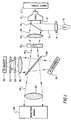
- a preferred embodiment for the overall system of the present invention is shown in FIG. 1.
- a video image signal source 2 provides an electrical signal which controls a raster scan to produce a desired video image.
- Signal source 2 can be obtained from various video imaging mechanisms, such as a video tape or a computer image generation system.
- the video signal can be arranged in any desired format, such as standard NTSC RS170.
- the video signal is applied to projector 4, which is a subsystem of the entire projection system and produces a substantially flicker-free output optical image.
- the term "optical” is intended to mean non-IR and non-UV, and generally visible light.
- Projector 4 is preferably implemented with the Sodern Visualization System produced by the Sodern Company of Lineil Brevannes Cedex, France. Details of this particular video projector are provided hereinafter.
- An optical beam 6 is formed from a low power intensity stabilized light source such as lamp 8, collimated by lens 9 and projected onto a polarizing beam splitter 10.
- This latter device provides the combined functions of splitting beam 6 and re-directing a portion of it onto projector 4 as an input readout beam 12, polarizing the readout beam 12, and cross-polarizing the output readout beam which is returned back from projector 4 along the path of the input beam 12.
- This cross-polarization function in effect analyzes the output readout beam from the projector, such that the spatial intensity of the output beam transmitted through polarizing beam splitter 10 varies in accordance with the degree of rotation of the output beam's polarization with respect to the initial polarization of input readout beam 12.
- Polarizing beam splitter 10 is provided as part of the Sodern Visualization System. It could be replaced by a separate beam splitter, input polarizer and output cross-polarizer, but it is preferable to use a device which combines these three functions in one. Commercially available calcite polarizes could also be used for the visible polarizer.
- Projector 4 operates upon the input polarized beam 12 to reflect an output beam along the same path as beam 12, but with a spatial polarization pattern determined by the video image signal from signal source 2.
- Polarizing beam splitter 10 transmits only those portions of the output beam whose polarization has been rotated in accordance with the video signal.
- An output optical beam 14 which carries the desired video image is thereby transmitted by the polarizing beam splitter.
- a lens 16, fiber optic bundle or a combination thereof directs the video image from projector 4 onto the input side of an LCLV 18.
- the lens will normally be used to magnify the video image so that it fills the available area on the LCLV, and should also be designed in accordance with standard optical principles to provide a uniform intensity and maintain the image resolution.
- the LCLV 18 is designed to impose an optical input image onto a readout IR or UV beam.
- the preferred form for the LCLV is described in a presentation by S.T. Wu, U. Efron, J. Grinberg, L.D. Hess and M.S. Welkowsky, "Infrared Liquid Crystal Light Valve", Proceedings of the International Society for Optical Engineering , Vol. 572 (1985), pages 94-101; further details are provided below.
- the present invention is operable with an LCLV readout beam with wavelength in the IR or UV region of the spectrum.
- LCLV readout beam with wavelength in the IR or UV region of the spectrum.
- the following description will refer only to IR readout beam for ease of explanation. This is not to be construed as a limitation.
- the IR beam upon which the video image is to be imposed is derived from a suitable IR source 20, a spectral filter 22 which selects the desired IR waveband, and a pre-polarizer element 24.
- a lens 26 converges the IR radiation transmitted from the above elements onto an IR polarizing beam splitter 28, which splits and polarizes the IR beam.
- a portion of the split IR beam is directed onto LCLV 18 as a readout beam 30, while the remainder of the IR beam is absorbed by absorption element 32.
- LCLV 18 includes a liquid crystal layer which may be visualized as being divided into pixel elements, with the liquid crystals of each pixel rotated in accordance with the localized intensity of the applied optical video image.
- the readout beam 30 passes through the LC layer and is reflected back upon itself (for a double pass). Thus, the readout beam 30 acquires a pattern of polarization rotations dependent upon the LC rotations of all of the pixels.
- the IR image beam 34 is formed having the video image information of the video image signal source 2.
- Polarizing beam splitter 28 could be replaced with a separate beam splitter and polarizing element, but a unitary device is preferred. A suitable device is described in U.S. Patent No. 4,049,944, "Process for Fabricating Small Geometry Semiconductive Devices Including Integrated Components", by Garvin, Yariv and Somekh, issued September 20, 1977 and assigned to Hughes Aircraft Company, the assignee of the present invention.
- the output IR beam 34 is directed by a collimating lens 36 onto a detector array or "seeker" 38.
- the optical image provided by a quality projector 4 is substantially flicker-free, and this characteristic is preserved by LCLV 18 to produce a substantially flicker-free output IR beam 34.
- the IR beam will also retain the high resolution of projector 4. Since the LCLV 18 requires only about 100 microwatts/cm2 of writing intensity, the optical source 8 used to read the projector 4 can be a relatively low intensity lamp of approximately 100 watts power rating, with a high degree of intensity stability.
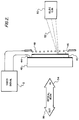
- FIG. 2 A simplified diagram of a preferred type of projector (of which the Sodern projection is an example) is shown in FIG. 2.
- the projector includes a high impedance solid electro-optic crystal 40 which is at least partially transparent to the wavelength of the light from lamp 8 as the basic beam-modulating element.
- the crystal impedance is high enough, generally in excess of 1012 ohm/sq., to prevent any substantial spreading of charge deposited upon its surface.
- the crystal is formed from deuterated potassium di-phosphate (DKDP).
- LiNbO3 Lithium niobate
- LiNbO3 LiNbO3
- DKDP has the advantage of requiring a substantially lesser voltage than LiNbO3 for a given level of birefringence.
- the birefringence of the DKDP crystal which depends on the wavelength, however, is too low to produce IR images.
- the crystal is mounted on a substrate 42 which is generally transparent to the optical wavelength.
- a transparent electrode 44 is located at the interface between the crystal 40 and substrate 42, while a dielectric mirror 46 coats the opposite side of the crystal away from the substrate.
- a fine conductive grid 48 is positioned spaced apart from the crystal, adjacent to the face with the dielectric mirror 46.
- the video image signal from video signal source 2 is applied across the grid 48 and electrode 44.
- An electron gun 50 directs a substantially constant intensity electron beam 52 across the mirrored crystal surface in a raster scan, with the beam penetrating the grid 48 just before reaching the crystal.
- an electron cloud which is brought by the beam and created by secondary emission from the crystal works like a local short circuit between the grid and the adjacent crystal surface. A localized charge is thus transferred onto the crystal surface in an amount determined by the instantaneous grid video signal voltage.
- a charge pattern is produced on the crystal surface which corresponds to the desired video image.
- This charge pattern is updated each time the beam completes a scanning pattern, and thus represents a real-time video image.
- the result is a shifting of the video image to a corresponding voltage pattern across the crystal.
- This process in general is independent of the previous grid voltage, permitting writing of charge onto the crystal and erasing to occur simultaneously.
- the high crystal impedance prevents any significant charge spreading or dissipation between successive scans, thereby causing the crystal spatial voltage pattern to be substantially constant and flicker-free.
- the crystal surface which receives the charges may be considered to be composed of an array of pixels.
- the crystal birefringence behind each pixel varies in accordance with the voltage across the crystal at that pixel.
- the charge pattern applied to the crystal induces a corresponding pattern of localized birefringence.
- This imposes the pixel pattern onto polarized light transmitted through the crystal, with the polarization rotated at each pixel by an amount which varies with the crystal's birefringence at that location.
- the video image pattern which is first represented on the grid by a varying voltage signal in coordination with the electron beam scanning is transferred in the form of a spatial polarization rotation pattern onto a polarized light beam transmitted through the crystal.
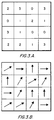
- FIG. 3(a) illustrates a matrix of pixels on the charged crystal surface, with the relative amount of charge at each pixel indicated by the numbers within the pixel squares.
- Numeral 3 represents maximum charge, while zero represents no applied charge.
- FIG. 3(b) Assuming that a vertically polarized beam is transmitted through the crystal, the resulting polarization pattern of the output beam is indicated in FIG. 3(b). It can be seen that those pixels having zero charge do not effect the vertical polarization orientation, those pixels with maximum charge have their polarization rotated 90°, and the pixels with intermediate amounts of charge have their polarization rotated by corresponding amounts.
- a polarized input beam 54 is directed through substrate 42, electrode 44 and crystal 40 onto the dielectric mirror 46; this beam corresponds to input readout beam 12 from the polarizing beam splitter 10 in FIG. 1.
- the polarization of the input beam 54 is rotated at each pixel location during transit through the crystal by an amount corresponding to the local crystal charge.
- the beam is reflected off mirror 46 and travels back through the crystal, receiving a further polarization rotation, to emerge as an output beam 56 having a spatial polarization rotation pattern which corresponds to the video image.
- This is the output beam which is transmitted through and processed by polarizing beam splitter 10 in FIG. 1, to emerge as optical video image beam 14.
- the input and output beams 54 and 56 are shown as being relatively small in diameter, in practice they would extend across substantially the entire crystal surface.
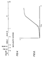
- the portions of the electromagnetic spectrum on either side of the visible region, over which the invention is intended to operate, are shown in FIG. 4.
- the visible spectrum extends from a wavelength of about 0.4 to about 0.7 microns.
- the next longer wavelengths lie in the IR regime, while the next shorter wavelengths are in the UV regime.
- the invention is adaptable to both the IR and UV regimes.
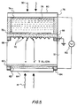
- FIG. 5 a sectional view of the preferred implementation of LCLV 18 for use with an IR output beam is given.
- the optical image beam 14 from projector 4 and lens 16 is applied to the input side of the device, while the IR readout beam 30 is applied to the readout side.
- a layer of high resistivity silicon photoconductor 58 has a thin p+ back contact layer 60 formed on its input side. This back contact provides a high sheet conductivity to present a very small load at any point in the device's cross-section where carriers are generated. The sensitivity and resolution of the device do not fluctuate with the input light level.
- An SiO2 oxide layer 62 may optionally be provided on the input side of back contact 60, followed optionally by an optical cement 64.
- a DC-biased n-type diode guard ring 66 is implanted at the opposite edge of the silicon photoconductor wafer 58 from back contact 60 to prevent peripheral minority carrier injection into the active region of the device.
- An SiO2 gate insulator layer 68 is formed on the readout side of the silicon photoconductor wafer 58. Isolated potential wells are created at the Si/SiO2 interface by means of an n-type microdiode array 70. This prevents the lateral spread of signal electrons residing at the interface.
- a reflective metal matrix mirror 72 is located on the readout side of the gate oxide layer 68 to provide broad-band IR reflectivity.
- the matrix nature of the mirror provides for very high ( ⁇ 1012 ohms/sq.) surface resistivity. Because the incident IR radiation is below the band gap of the Si photoconductor, it does not create photocharge in the photoconductor.
- a thin film of fast response liquid crystal 74 is employed as the light modulating electro-optic layer on the readout side of mirror 72.
- a front IR transparent material 76 either Ge which is inherently conductive, or Si implanted at the liquid crystal side for a conductive electrode 78, is placed adjacent the liquid crystal. The front of plate 76 is coated with an anti-reflection coating 80, and the whole structure is assembled within an airtight anodized aluminum holder.
- Silicon photoconductor 58 is coupled with oxide layer 68 and transparent "metallic" (conductive) electrode coating 78 to form an "MOS" structure.
- the combination of the insulating liquid crystal, oxide and mirror act as the insulating gate of the MOS structure.
- an alternating voltage source 82 is connected on one side to back contact 60 by means of an aluminum back contact pad 84, and on its opposite side to counterelectrode 78.
- the voltage across the two electrodes causes the MOS structure to operate in alternate depletion (active) and accumulation (inactive) phases.
- the depletion phase the high resistivity silicon photoconductive layer 58 is depleted and electron-hole pairs generated by input optical image beam 14 are swept by the electric field in the photoconductor, thereby produci.ng a signal current that activates the liquid crystal.
- the electric field existing in the depletion region acts to sweep the signal charges from the input side to the readout side, and thus preserves the spatial resolution of the input image.
- the alternating voltage source 82 To avoid modulation of the effect of the liquid crystal, and "flicker" in the output, it is only necessary that the alternating voltage source 82 have a modulation frequency high enough that the liquid crystal only responds to an average voltage. This condition is easily satisfied.
- the polarized IR readout beam 30 enters the readout side of the light valve through transparent layer 76, passes through the liquid crystal layer 74, and is reflected by metal matrix mirror 72 back through the liquid crystal. Since the conductivity of each pixel in photoconductive layer 58 varies with the intensity of input optical beam 14 at that pixel, a voltage divider effect results which varies the voltage across the corresponding pixel of the liquid crystal in accordance with the spatial intensity of the input light.
- the liquid crystals at any location will orient themselves in accordance with the impressed voltage, and the liquid crystal orientation relative to the readout beam polarization at any particular location will determine the amount of reflected readout radiation that will be transmitted by the analyzer.
- the spatial intensity pattern of the input light is transferred to a spatial liquid crystal orientation pattern in the liquid crystal layer, which in turn controls the spatial polarization of the IR readout beam which finally controls the spatial intensity of the IR beam transmitted by the analyzer.
- LCLV 18 preserves the substantially flicker-free condition of input optical beam 14 as it is transferred onto the IR readout beam 30.
- Detector array 38 is thus presented with a desirable IR video image that is substantially flicker-free, and can be varied in real-time.
- UV light is at a higher energy level than the Si bandgap and would create photoelectrons after passage through the gaps of the metal matrix mirror.
- Typical dielectric mirrors used for visible light LCLVs have low reflectivity in the UV.
- the desired characteristics for a UV mirror would be that its reflection be essentially 100%, its transmission be essentially zero (not more than 10 ⁇ 6), its sheet resistivity be very high (greater than about 1010 ohm/sq) to prevent image charge spreading, and its bulk resistivity be low so that little of the photo generated voltage is taken from the liquid crystal by the mirror.
- a mirror suitable for a UV LCLV is not yet known to have been implemented, but it is believed that such dielectric mirrors could be successfully fabricated with appropriate investigation of the component materials.
- FIG. 6 A typical current-voltage response curve for an LCLV is shown in FIG. 6. Appreciable modulation of the device's readout beam does not occur until the applied voltage across the liquid crystal exceeds a threshold level V th . This phenomenon is utilized in accordance with the invention to further reduce flicker and improve the output image quality.
- the time required to WRITE charge onto or ERASE charge from a pixel on the crystal is discussed below.
- the ERASE operation which occurs when a zero or low voltage frame follows a higher voltage frame and dissipates charge from the crystal, occurs fairly rapidly.
- the time required to fully WRITE charge onto a crystal pixel is considerably longer.
- an ERASE operation may be nearly completed during a single frame, while a WRITE may be significantly incomplete.
- the ERASE and WRITE curves are also generally reversed.
- the WRITE operation is now completed fairly rapidly, while the ERASE operation takes considerably more time.
- the corresponding pixel of the light valve readout beam will not be modulated.
- the rapid WRITE of charge onto the crystal is used to produce a correspondingly high degree of responsiveness in the light valve, while the relatively slower ERASE operation in the projector does not materially effect the responsiveness of the light valve.
- the Sodern projector employs a light source that is quite bright, a 4.5 kW xenon arc lamp. This type of source is generally unstable, and can produce flicker. When the Sodern projector is used in connection with an appropriate light valve as described above, this bright light source can be replaced with a low intensity, highly stable source.
- a 100 Watt xenon arc lamp with a regulated power supply can be used to yield an intensity stability of about 0.2%; a quartz halogen lamp could also be used for the source. With either of these low power sources, the optics should be adjusted to provide a substantially uniform illumination of the crystal.
Landscapes
- Engineering & Computer Science (AREA)
- Multimedia (AREA)
- Signal Processing (AREA)
- Health & Medical Sciences (AREA)
- Biomedical Technology (AREA)
- General Health & Medical Sciences (AREA)
- Liquid Crystal (AREA)
- Liquid Crystal Display Device Control (AREA)
- Transforming Electric Information Into Light Information (AREA)
- Transforming Light Signals Into Electric Signals (AREA)
Claims (9)
- Ein System zum Modulieren eines Infrarot- (IR) oder Ultraviolettstrahls (UV) (30), um ein im wesentlichen flimmerfreises Videozielbild (34) bereitzustellen, mit:a) einem Videoprojektor (4), der aufweist:1) einen elektro-optischem Kristall (40) mit ersten und zweiten einander gegenüberliegenden Oberflächen und einer Impedanz, die genügt, substantielles Verschmieren von lokalisierten elektrischen Ladungen auf dem Kristall zu verhindern, wobei der Kristall in einem vorbestimmten Lichtwellenband wenigstens teilweise transparent ist,2) ein leitfähiges Gitter (48) benachbart aber mit Abstand zu der ersten Kristalloberfläche,3) eine Einrichtung (2, 44) zum belegen eines Videospannungssignals zwischen dem leitfähigen Gitter (48) und dem Kristall,4) eine Elektronenkanone (50), angeordnet, um die erste Kristalloberfläche in Synchronität mit dem Videospannungssignal abzutasten, wobei der Elektronenstrahl (52) einen leitenden Pfad zwischen dem leitfähigen Gitter (48) und dem Teil der ersten Kristalloberfläche unter dem Elektronenstrhal herstellt, um eine lokalisierte Ladung zu der Kristalloberfläche zu übertragen und um in dem Kristall (40) eine entsprechende lokalisierte Doppelbrechung zu induzieren, wobei der Betrag des Ladungsübertrags durch das Viedospannungssignal an dem leitfähigen Gitter zum Zeitpunkt des Übertrags kontrolliert wird, wobei der Elektronenstrahl (52) ein Videomuster mit lokalisierten Ladungen auf der ersten Kristalloberfläche und ein entsprechendes Muster aus lokalisierten Bereichen mit Doppelbrechung in dem Kristall (40) formt, während die Abtastung in Synchronität mit dem Videospannungssignal fortschreitet, und5) einen Spiegel (46), der angeordnet ist, Licht durch den Kristall (40) zurück zu reflektieren, das von der zweiten Kristalloberfläche durch den Kristall (40) hindurch übertragen wird;b) einer Polarisationseinrichtung (10), um einen optischen Eingangsstrahl (12) zu polarisieren, der wenigstens teilweise das vorbestimmte Lichtwellenband umfaßt und von der zweiten Kristalloberfläche durch den Kristall (40) hindurch gerichtet wird, um das Polarisationsmuster eines reflektierten Strahles (56), zurückreflektiert von dem optischen Eingangsstrahl (56 54) durch den Kristall (40) hindurch, zu analysieren, und um einen Ausgangsstrahl zu übertragen, der ein Videomuster des reflektierten Strahls enthält, wobei das Videomuster einem Polarisationsdrehmuster entspricht, das dem reflektierten Strahl (56) durch das Muster mit lokalisierten Bereichen mit Doppelbrechung aufgeprägt worden ist; undc) einem Flüssigkristallichtventil (LCLV) (18) angeordnet, den Videoprojektorausgangsstrahl (14) als einen Steuerungseingang für das LCLV (18) zu empfangen, und einen IR- oder UV-Auslesestrahl (30), mit dem das LCLV (18) beaufschlagt wird, entsprechend dem durch den Videoprojektorausgangsstrahl (14) getragenen Videomuster zu modulieren, wobei das LCLV (18) den Videoprojektorausgangsstrahl (14) in ein räumliches Spannungsmuster umwandelt und den IR- oder UV-Auslestrahl (30) entsprechend jedem Teil des räumlichen Spannungsmusters, das einen Spannungsschwellenwert übersteigt, moduliert, und wobei der Videoprojektor (4) unterschiedliche SCHREIB- und LÖSCH-Perioden aufweist, wenigstens eine davon länger als die Bildrahmenperiode des Videozielbildes ist, die Identität der längeren Periode von der Spannungspolarität abhängt, die an das leitfähige Gitter (48) angelegt wird, wobei die Einrichtung (2, 44) zum Anlegen des Videospannungssignals zwischen dem leitfähigen Gitter (48) und dem Kristall (40) eine Spannungspolarität an das leitfähige Gitter (48) anlegt, die eine kürzere SCHREIB-Periode erzeugt, das LCLV (18) eine Antwortzeit hat, derart, daß sein räumliches Spannungsmuster unter seinem Spannungsschwellenwert zum Ende der LÖSCH-Periode von dem Videoprojektor (4) liegt, wodurch das LCLV (18) zu solchen Zeiten gehindert wird, den IR- oder UV-Auslesestrahl (30) zu modulieren, selbst wenn der Videoprojektorausgangsstrahl (14) und das räumliche LCLV-Spannungsmuster größer als null sind.
- Das System zum Modulieren eines Strahls nach Anspruch 1, desweiteren eine optische Einrichtung (16) umfassend, angeordnet zwischen der Polarisationseinrichtung (10) und dem LCLV (18), um den Ausgangsstrahl (14) auf das LCLV (18) zu lenken.
- Ein System zum Erzeugen eines Videobildes im Infraroten (IR) oder im Ultravioletten (UV), mit:
einem Videoprojektorsystem (2, 4, 6, 8, 9, 10, 12, 14, 16) zum Erzeugen eines im wesentlichen flimmerfreien optischen Videobildes als Antwort auf ein Eingangsvideosignal,
einem Flüssigkristall-Lichtventil (LCLV) (18) mit einer Einrichtung zum Empfangen eines optischen Eingangsbildes und einer Einrichtung zum Modulieren eines IR- oder UV-Auslesestrahls (30), mit dem das LCLV (18) mit dem optischen Eingangsbild beaufschlagt wird,
einer optischen Einrichtung (16) zum Lenken des optischen Videobildes von dem Videoprojektor (4) auf das LCLV (18) als das optische Eingangsbild,
einer IR- oder UV-Quelle (20), und
Einrichtungen (22, 24, 26, 28) zum Beaufschlagen von Strahlung von der IR- oder UV-Quelle (20) auf das LCLV (18) als der IR- oder UV-Auslesestrahl (30), wobei der IR- oder UV-Auslesestrahl (30) das IR- oder UV-Videobild von dem LCLV (18) abnimmt,
wobei das LCLV (18) das optische Videobild von dem Projektor (4) in ein räumliches Spannungsmuster umwandelt und den IR- oder UV-Auslesestrahl (30) entsprechend jedem Teil des räumlichen Spannungsmusters, das einen Spannungsschwellenwert übersteigt, moduliert, das LCLV (18) eine LÖSCH-Antwortzeit aufweist, derart, daß sein räumliches Spannungsmuster unter seinem Spannungsschwellenwert zu ende einer LÖSCH-Periode von dem optischen Videobild liegt, wodurch das LCLV (18) zu solchen Zeiten geändert wird, den IR- oder UV-Auslesestrahl (30) zu modulieren, selbst wenn das optische Videobild und das räumliche LCLV-Spannungsmuster größer als null sind. - Das Videobildsystem nach Anspruch 3, wobei das Videoprojektorsystem (2, 4, 6, 8, 9, 10, 12, 14, 16) aufweist:
einen elektro-optischen Kristall (40) mit einer Impedanz, die genügt, substantielles Verschmieren von darauf befindlicher Ladung zu verhindern,
Einrichtungen (2, 44, 48, 50) zum Ablagern von Ladungspixeln auf dem Kristall (40) in einem Muster entsprechend einem gewünschten Videobild, wobei die Ladungspixel ein Muster von lokalisierten Doppelbrechungen in dem Kristall (40) erzeugen,
eine Lichtquelle (8),
eine Einrichtung (9) zum Formen des Lichts aus der Lichtquelle (8) in einem Auslesestrahl (12) für den Videoprojektor,
eine Einrichtung zum Transmittieren des Projektorauslesestrahls (12) durch den Kristall (40), um ein Polarisationsmuster zu erlangen, das dem Muster aus lokalisierten Doppelbrechungen im Kristall entspricht, und
eine Einrichtung (10) zum Polarisieren des Projektorauslesestrahls (12) vor der Übertragung durch den Kristall (40) und zum Analysieren des Projektorauslesestrahls (12) nach der Übertragung durch den Kristall (40), um das IR- oder UV-Videobild zu erzeugen. - Das Videbildsystem nach Anspruch 4, worin die Lichtquelle (8) hinsichtlich Intensitätsschwankungen stabilisiert ist.
- Ein Verfahren zum Formen eines Infrarot (IR)- oder Ultraviolett (UV)-Strahls (34) mit einem im wesentlichen flimmerfreien Videobild, mit:
Beaufschlagen eines elektro-optischen Kristalls (40) mit Ladungspixeln in einem Muster, das einem gewünschten Videobild entspricht, und wodurch ein Doppelbrechungsmuster in dem Kristall (40) erzeugt wird, das ebenfalls dem gewünschten Videobild entspricht, wobei der Kristall eine Impedanz aufweist, die groß genug ist, wesentliches Verschmieren der aufgebrachten Ladung zu verhindern,
Auslesen des Kristall-Doppelbrechungsmusters mit einem polarisierten Kristall-Auslesestrahl (12) in dem der polarisierte Kristall-Auslesestrahl durch den Kristall (40) hindurch übertragen wird und dann durch einen Kreuzpolarisator (10) geführt wird,
Zuführen des polarisierten Kristall-Auslesestrahls (12) nach Übertragung durch den Kristall (40) und Bearbeitung durch den Kreuzpolarisator (10) als ein Videoeingang (14) zu einem Flüssigkristall-Lichtventil (LCLV) (18),
Zuführen eines polarisierten IR- oder UV-Auslesestrahls (30) zu dem LCLV (18), und
Steuern des LCLV (18), so daß sein Videoeingang auf den IR- oder UV-LCLV-Auslesestrahl (30) übertragen wird,
wobei das LCLV (18) seinen Videoeingang in ein räumliches Spannungsmuster umwandelt und den IR- oder UV-LCLV-Auslesestrahl (30) entsprechend jedem Teil des räumlichen Spannungsmusters, das einen Spannungsschwellenwert übersteigt, moduliert, wobei das LCLV (18) einen LÖSCH-Antwortzeit aufweist, derart, daß sein räumliches Spannungsmuster unter seinem Spannungsschwellenwert zum Ende der LÖSCH-Periode von demgewünschten Videobild liegt, wodurch das LCLV (18) zu solchen Zeiten gehindert wird, den IR- oder UV-Auslesestrahl (30) zu modulieren, selbst wenn das gewünschte Videobild und das räumliche Spannungsmuster des LCLV größer als 0 sind. - Das Verfahren nach Anspruch 6, worin die Ladungspixel dem Kristal (40) zugeführt werden, in dem ein leitfähiges Gitter (48) benachbart zu dem Kristall (40) positioniert wird, zwischen dem Gitter (48) und dem Kristall (40) ein Videospannungssignal angelegt wird, und der Kristall (40) mit einem Elektronenstrahl (52) synchron mit dem Videospannungssignal abgetastet wird.
- Das Verfahren nach Anspruch 7, worin das Videospannungssignal geändert wird, um das Muster von Ladungspixeln auf dem Kristall (40) zu ändern.
- Das Verfahren nach Anspruch 6, worin der polarisierte Lichtauslesestrahl (12) eine Leistung in der Größenordnung von 100 Watt aufweist.
Applications Claiming Priority (2)
| Application Number | Priority Date | Filing Date | Title |
|---|---|---|---|
| US137543 | 1987-12-23 | ||
| US07/137,543 US4894724A (en) | 1987-12-23 | 1987-12-23 | System and method for producing a flicker-free video image |
Publications (2)
| Publication Number | Publication Date |
|---|---|
| EP0348499A1 EP0348499A1 (de) | 1990-01-03 |
| EP0348499B1 true EP0348499B1 (de) | 1993-04-14 |
Family
ID=22477897
Family Applications (1)
| Application Number | Title | Priority Date | Filing Date |
|---|---|---|---|
| EP89902359A Expired - Lifetime EP0348499B1 (de) | 1987-12-23 | 1988-11-21 | System und verfahren zur erzeugung eines flimmer-freien bildes |
Country Status (6)
| Country | Link |
|---|---|
| US (1) | US4894724A (de) |
| EP (1) | EP0348499B1 (de) |
| JP (1) | JPH02503044A (de) |
| DE (1) | DE3880310T2 (de) |
| IL (1) | IL88466A (de) |
| WO (1) | WO1989006081A2 (de) |
Families Citing this family (8)
| Publication number | Priority date | Publication date | Assignee | Title |
|---|---|---|---|---|
| US5374954A (en) * | 1990-10-11 | 1994-12-20 | Harry E. Mowry | Video system for producing video image simulating the appearance of motion picture or other photographic film |
| US5610735A (en) * | 1993-06-04 | 1997-03-11 | Matsushita Electric Industrial Co., Ltd. | Light scattering light valve projection apparatus |
| EP0762370A3 (de) * | 1995-08-02 | 1998-01-07 | Canon Kabushiki Kaisha | Ansteuerungsverfahren für ein Anzeigegerät mit optischer Modulationsvorrichtung |
| US6005692A (en) * | 1997-05-29 | 1999-12-21 | Stahl; Thomas D. | Light-emitting diode constructions |
| US20040178975A1 (en) * | 2003-03-10 | 2004-09-16 | George Benedict | Method and apparatus for displaying a picture from an optical birefringence recording |
| US20100096553A1 (en) * | 2008-10-22 | 2010-04-22 | Honeywell International Inc. | Reflective optical sensor and switches and systems therefrom |
| DE102013003660A1 (de) * | 2013-03-02 | 2014-09-04 | Mbda Deutschland Gmbh | Optische Vorrichtung |
| US9575340B2 (en) * | 2015-02-24 | 2017-02-21 | Ii-Vi Incorporated | Electrode configuration for electro-optic modulators |
Family Cites Families (8)
| Publication number | Priority date | Publication date | Assignee | Title |
|---|---|---|---|---|
| US3637931A (en) * | 1968-12-20 | 1972-01-25 | Philips Corp | Optic relay for use in television |
| DE2103542A1 (de) * | 1970-01-26 | 1971-08-12 | Thomson Csf | Kraftmeßvorrichtung |
| US4127322A (en) * | 1975-12-05 | 1978-11-28 | Hughes Aircraft Company | High brightness full color image light valve projection system |
| US4049994A (en) * | 1976-01-26 | 1977-09-20 | Rca Corporation | Light emitting diode having a short transient response time |
| US4018509A (en) * | 1976-03-08 | 1977-04-19 | Hughes Aircraft Company | Optical data processing system with reflective liquid crystal light valve |
| US4113367A (en) * | 1976-09-09 | 1978-09-12 | Ulrich M. Fritzler | Roof reflective polygon scanning apparatus |
| US4389096A (en) * | 1977-12-27 | 1983-06-21 | Matsushita Electric Industrial Co., Ltd. | Image display apparatus of liquid crystal valve projection type |
| US4611245A (en) * | 1984-10-29 | 1986-09-09 | The United States Of America As Represented By The Secretary Of The Navy | Real-time ultra-high resolution image projection display using laser-addressed liquid crystal light valve |
-
1987
- 1987-12-23 US US07/137,543 patent/US4894724A/en not_active Expired - Fee Related
-
1988
- 1988-11-21 DE DE8989902359T patent/DE3880310T2/de not_active Expired - Fee Related
- 1988-11-21 WO PCT/US1988/004145 patent/WO1989006081A2/en not_active Ceased
- 1988-11-21 JP JP1502235A patent/JPH02503044A/ja active Pending
- 1988-11-21 EP EP89902359A patent/EP0348499B1/de not_active Expired - Lifetime
- 1988-11-23 IL IL8846688A patent/IL88466A/en not_active IP Right Cessation
Non-Patent Citations (3)
| Title |
|---|
| 1985 SID INTERNATIONAL SXMPOSIUM, Digest of Technical Papers, 1st edition, May 1985, Palisades Institute for Research Services, Inc., New York, US; A. FARRAYRE et al.: "Geometrical resolution improvement of sodern visualization system", pages 266-269. * |
| OPTICAL ENGINEERING, volume 22, no.6, November/December 1983, Society of Photo-Optical Instrumentation Engineers, Bellingham, Washington, US; U. EFRON et al.: "Silicon liquid crystal light valves : status and issues", pages 682-686. * |
| SPIE, volume 940, 4-6 April 1988, W. LEE et al.: "Flickerless dynamic IR scene generation for simulation applications", pages 176-181. * |
Also Published As
| Publication number | Publication date |
|---|---|
| JPH02503044A (ja) | 1990-09-20 |
| DE3880310D1 (de) | 1993-05-19 |
| WO1989006081A2 (en) | 1989-06-29 |
| WO1989006081A3 (en) | 1989-07-13 |
| DE3880310T2 (de) | 1993-07-29 |
| IL88466A (en) | 1994-02-27 |
| US4894724A (en) | 1990-01-16 |
| EP0348499A1 (de) | 1990-01-03 |
Similar Documents
| Publication | Publication Date | Title |
|---|---|---|
| US4481531A (en) | Microchannel spatial light modulator | |
| US3723651A (en) | Optically-scanned liquid-crystal projection display | |
| US3627408A (en) | Electric field device | |
| AU661501B2 (en) | Membrane light modulating systems | |
| EP0289544B1 (de) | Durch einen elektronenstrahl adressiertes flüssigkristall-lichtventil | |
| US3001447A (en) | Image reproducing device for visible and invisible radiation images | |
| US4533215A (en) | Real-time ultra-high resolution image projection display using laser-addressed liquid crystal light valve | |
| EP0394674B1 (de) | Element zur Lichtumwandlung und eine Abbildungsvorrichtung | |
| EP0303686B1 (de) | Elektronenstrahl angesteuertes flüssigkristallichtventil mit flächenkaftem eingabeleiter | |
| US4158201A (en) | Flat electro optic display panel and method of using same | |
| EP0348499B1 (de) | System und verfahren zur erzeugung eines flimmer-freien bildes | |
| EP0309574B1 (de) | Lichtventilvorrichtung und methode zum pulsweisen auslesen | |
| EP0517517A1 (de) | Aus einem einzelnen Lichtventil bestehender Vollfarbenprojektor | |
| US3308233A (en) | Xerographic facsimile printer having light beam scanning and electrical charging with transparent conductive belt | |
| US2681380A (en) | Color television projection system | |
| US4013345A (en) | Deformable mirror light valve and method of operating the same | |
| US3629499A (en) | Pattern noise reduction system | |
| US6123288A (en) | Apparatus and method for flickerless projection of infrared scenes | |
| Donjon et al. | A Pockels-effect light valve: Phototitus. Applications to optical image processing | |
| US3601468A (en) | Optical light wave modulator for representing a first color light wave as a second color light wave | |
| GB1374740A (en) | Cathode ray tube display | |
| US2577756A (en) | Color television | |
| US5210628A (en) | Liquid crystal light valve with photosensitive layer having irregular diode pattern | |
| EP0403307B1 (de) | Verfahren zur Steuerung eines opto-optischen Wandlers | |
| US3352967A (en) | Image projection system having electrically charged tape and electro-optical crystal |
Legal Events
| Date | Code | Title | Description |
|---|---|---|---|
| PUAI | Public reference made under article 153(3) epc to a published international application that has entered the european phase |
Free format text: ORIGINAL CODE: 0009012 |
|
| 17P | Request for examination filed |
Effective date: 19890805 |
|
| AK | Designated contracting states |
Kind code of ref document: A1 Designated state(s): DE FR GB IT NL |
|
| 17Q | First examination report despatched |
Effective date: 19910712 |
|
| GRAA | (expected) grant |
Free format text: ORIGINAL CODE: 0009210 |
|
| AK | Designated contracting states |
Kind code of ref document: B1 Designated state(s): DE FR GB IT NL |
|
| REF | Corresponds to: |
Ref document number: 3880310 Country of ref document: DE Date of ref document: 19930519 |
|
| ET | Fr: translation filed | ||
| ITF | It: translation for a ep patent filed | ||
| PLBE | No opposition filed within time limit |
Free format text: ORIGINAL CODE: 0009261 |
|
| STAA | Information on the status of an ep patent application or granted ep patent |
Free format text: STATUS: NO OPPOSITION FILED WITHIN TIME LIMIT |
|
| 26N | No opposition filed | ||
| REG | Reference to a national code |
Ref country code: GB Ref legal event code: 732E |
|
| PGFP | Annual fee paid to national office [announced via postgrant information from national office to epo] |
Ref country code: NL Payment date: 19981028 Year of fee payment: 11 |
|
| PG25 | Lapsed in a contracting state [announced via postgrant information from national office to epo] |
Ref country code: NL Free format text: LAPSE BECAUSE OF NON-PAYMENT OF DUE FEES Effective date: 20000601 |
|
| NLV4 | Nl: lapsed or anulled due to non-payment of the annual fee |
Effective date: 20000601 |
|
| REG | Reference to a national code |
Ref country code: FR Ref legal event code: TP Ref country code: FR Ref legal event code: CD Ref country code: FR Ref legal event code: CA |
|
| REG | Reference to a national code |
Ref country code: GB Ref legal event code: IF02 |
|
| PGFP | Annual fee paid to national office [announced via postgrant information from national office to epo] |
Ref country code: FR Payment date: 20021010 Year of fee payment: 15 |
|
| PGFP | Annual fee paid to national office [announced via postgrant information from national office to epo] |
Ref country code: GB Payment date: 20021016 Year of fee payment: 15 |
|
| PGFP | Annual fee paid to national office [announced via postgrant information from national office to epo] |
Ref country code: DE Payment date: 20021022 Year of fee payment: 15 |
|
| PG25 | Lapsed in a contracting state [announced via postgrant information from national office to epo] |
Ref country code: GB Free format text: LAPSE BECAUSE OF NON-PAYMENT OF DUE FEES Effective date: 20031121 |
|
| PG25 | Lapsed in a contracting state [announced via postgrant information from national office to epo] |
Ref country code: DE Free format text: LAPSE BECAUSE OF NON-PAYMENT OF DUE FEES Effective date: 20040602 |
|
| GBPC | Gb: european patent ceased through non-payment of renewal fee |
Effective date: 20031121 |
|
| PG25 | Lapsed in a contracting state [announced via postgrant information from national office to epo] |
Ref country code: FR Free format text: LAPSE BECAUSE OF NON-PAYMENT OF DUE FEES Effective date: 20040730 |
|
| REG | Reference to a national code |
Ref country code: FR Ref legal event code: ST |
|
| PG25 | Lapsed in a contracting state [announced via postgrant information from national office to epo] |
Ref country code: IT Free format text: LAPSE BECAUSE OF NON-PAYMENT OF DUE FEES;WARNING: LAPSES OF ITALIAN PATENTS WITH EFFECTIVE DATE BEFORE 2007 MAY HAVE OCCURRED AT ANY TIME BEFORE 2007. THE CORRECT EFFECTIVE DATE MAY BE DIFFERENT FROM THE ONE RECORDED. Effective date: 20051121 |