EP0348053B1 - Controlling the initiation of logical systems in a data processing system with logical processor facility - Google Patents
Controlling the initiation of logical systems in a data processing system with logical processor facility Download PDFInfo
- Publication number
- EP0348053B1 EP0348053B1 EP89305542A EP89305542A EP0348053B1 EP 0348053 B1 EP0348053 B1 EP 0348053B1 EP 89305542 A EP89305542 A EP 89305542A EP 89305542 A EP89305542 A EP 89305542A EP 0348053 B1 EP0348053 B1 EP 0348053B1
- Authority
- EP
- European Patent Office
- Prior art keywords
- processing unit
- facilities
- primary processing
- domain
- initiation
- Prior art date
- Legal status (The legal status is an assumption and is not a legal conclusion. Google has not performed a legal analysis and makes no representation as to the accuracy of the status listed.)
- Expired - Lifetime
Links
Images


Classifications
-
- G—PHYSICS
- G06—COMPUTING OR CALCULATING; COUNTING
- G06F—ELECTRIC DIGITAL DATA PROCESSING
- G06F9/00—Arrangements for program control, e.g. control units
- G06F9/06—Arrangements for program control, e.g. control units using stored programs, i.e. using an internal store of processing equipment to receive or retain programs
- G06F9/46—Multiprogramming arrangements
- G06F9/48—Program initiating; Program switching, e.g. by interrupt
- G06F9/4806—Task transfer initiation or dispatching
- G06F9/4843—Task transfer initiation or dispatching by program, e.g. task dispatcher, supervisor, operating system
-
- G—PHYSICS
- G06—COMPUTING OR CALCULATING; COUNTING
- G06F—ELECTRIC DIGITAL DATA PROCESSING
- G06F15/00—Digital computers in general; Data processing equipment in general
- G06F15/16—Combinations of two or more digital computers each having at least an arithmetic unit, a program unit and a register, e.g. for a simultaneous processing of several programs
- G06F15/177—Initialisation or configuration control
-
- G—PHYSICS
- G06—COMPUTING OR CALCULATING; COUNTING
- G06F—ELECTRIC DIGITAL DATA PROCESSING
- G06F9/00—Arrangements for program control, e.g. control units
- G06F9/06—Arrangements for program control, e.g. control units using stored programs, i.e. using an internal store of processing equipment to receive or retain programs
- G06F9/46—Multiprogramming arrangements
- G06F9/468—Specific access rights for resources, e.g. using capability register
Definitions
- This invention relates to a data processing system that supports concurrent operation of multiple system control programs.
- Each system control program in the data processing system operates in a separate domain of facilities as though it had the control of an individual, logical computer.
- the present invention relates to method and apparatus for controlling the initiation of a domain of facilities in such a data processing system.
- the features of a data processing system such as, for example, its maximum memory size or the allowable types of its input/output channel operations, are often sold or leased as options. Therefore, it is often desirable to be able to control features of a data processing system.
- one such important feature is the number of domains that can be initiated concurrently in the system. Controlling the number of domains is desirable, for example, when a system installation is charged for the maximum number of domains that can be activated concurrently or when it is desirable to guarantee a minimum level of performance of the domains by regulating system resources contention.
- controlling a feature of a system is achieved by storing an authorization code in a "hidden" location of the main memory.
- the authorization code may be, for example, the maximum number of domains that can be started concurrently.
- a key code (which, under the above example, will be the number of domains already activated in the system) will be checked against the authorization code. The feature operation will be changed when the check is successful.
- One disadvantage of the above-described method is that because the authorization code is stored in the main memory, it can easily be tampered with.
- EP-A-0099244 discloses a multi-processing system which is partitionable into different applications under software control while the subsystems of the system are permanently interconnected physically a subsystem access unit is provided to enable and disable the subsystem interconnections according to the required configuration.
- the subsystem access unit processor checks whether command sources issuing requests for partitioning are sources which are assigned to particular applications and on the basis of that check enables or disables interconnections to form partitions.
- the present invention provides a method for controlling the initiation of a domain in a computer system having at least one primary processing unit processing user tasks and an auxiliary processing unit servicing said at least one primary processing unit, said primary processing and having facilities, including processing and input/output devices, that allow concurrent operation of more than one system control program, each system control program being assigned a separate domain of facilities in which it operates as though it had control of an individual computer, said initiation being performed in response to a request signal, the method comprising the steps of: disabling one or more facilities that will be assigned to a system control system; providing an authorization code in a read-only device; generating a key code in response to said request; comparing said key code with said authorization code; and enabling said disabled facilities if said comparison satisfies one or more predefined criteria; characterized in that said authorization code is stored in said auxiliary processing unit (105) and is a function of the number of domains allowed to be initiated concurrently in the primary processing unit and said key code is a function of the number of domains already initiated in the primary processing
- the present invention also provides apparatus for controlling the initiation of a domain in a computer system having at least one primary processing unit processing user tasks and an auxiliary processing unit servicing said at least one primary processing unit said primary processing unit having facilities, including input/output channels, that allow concurrent operation of more than one system control program, each system control program being assigned a separate domain of facilities in which it operates as though it had control of an individual computer, said initiation being performed in response to a request signal, the apparatus comprising: means coupled to said facilities for disabling one or more facilities that will be assigned to a system control system; read-only storage means for storing an authorization code; generating means for generating a key code in response to said request; comparison means coupled to said read-only storage means and generating means for comparing said key code with said authorization code; and means responsive to said comparison means for enabling said disabled facilities if said comparison satisfies one or more predefined criteria; characterized in that said authorization code is stored in said auxiliary processing unit (105) and is a function of the number of domains allowed to be initiated concurrently
- An advantage of this invention is the provision of a more secure method and apparatus for controlling the number of domains which can be initiated in a multi-domain system.
- Fig. 1 is a block diagram of a computer system wherein the present invention is embodied.
- Fig. 2 is a schematic block diagram of a processor in the computer system of Fig. 1.
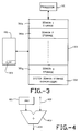
- Fig. 3 is a block diagram of the computer system of Fig. 1 when operating as a multi-domain system.
- Fig. 4 is a diagram illustrating the apparatus for translating domain address to absolute main memory address.
- Fig. 5 illustrates the load address modulation register (LAMR) operation of the computer system.
- Fig. 6. is a block diagram of the service processor connected to the computer system of Fig. 1.
- Fig. 1 illustrates a computer system 100 which is architecturally similar to the Amdahl 580 family of computers and the computer system described in the above-identified Doren et al application.
- Computer system 100 includes one or more processors 101a, 101b,..., 101n, and one or more input/output (I/O) channels 102a, 102b,..., 102m.
- a plurality of terminals 104a, 104b,..., 104k, including at least one operator terminal 104b, are connected to the computer system 100 via one or more of the channels 102a-102m.
- Each of the processors 101a-101n and channels 102a-102m is connected to the main memory 103.
- the computer system 100 is further connected to at least one service processor (SVP) 105.
- the service processor 105 is an independent processing unit that has its own memory, its own internal and external registers, and its own input and output ports.
- the interface 106 between the service processor 105 and the computer system 100 includes address, data, interrupt and control lines, whereby the service processor 105 scan and set latches of the computer system 100 and also storage locations of the main memory 103.
- the service processor 105 performs these functions using system control facilities that are similar to the SCAN and CIC facilities of the Amdahl 580 computers.
- the computer system 100 can signal the service processor 105 to perform certain functions, (e.g., taking a machine log or setting specific latches), by depositing a function code and required operands in an area called hardware storage area (HSA) 107, and by generating an interrupt signal to the service processor 105 in the interface 106.
- HSA hardware storage area
- the service processor 105 receives an interrupt from the computer system 100, it fetches the function code and associated operands or operand addresses from the hardware storage area (HSA) 107.
- the service processor then performs the functions according to the function code from the computer system.
- Fig. 2 illustrates the architecture of one of the processors 101a-101n of the computer system 100.
- Each of the processors 101a-101n in the computer system 100 is architecturally similar to the Amdahl 580 computer systems.
- Each such processor comprises an instruction unit (I-unit) 201, an execution unit (E-unit) 202 and a storage unit (S-unit) 203.
- the I-unit 201 is responsible for decoding an instruction and generating signals to control the execution of the instruction.
- An instruction supplied to the processor 101 is received by the I-unit 201, which generates a control store address in circuit 204 based upon the opcode of the instruction.
- the control store address is used to fetch a microprogram instruction from the control store 205.
- the fetched microprogram instruction is supplied to a decoder 206 wherein a plurality of control signals are generated.
- the control signals generated by the decoder 206 include address signals and control signals which are supplied to an effective address generator.
- the control signals causes the effective address generator to generate effective addresses of the operands based upon the respective address fields, such as a base field, an index field and a displacement field specified in the instruction.
- the I-unit 201 also generates control signals to the S-unit 203 which fetches the operands based upon the effective addresses generated from the E-unit 202.
- the I-unit 201 also generates control signals to the E-unit 202 which, in response to the control signals, performs an exception check on the operands, and/or predefined operations on the operands.
- control signals generated by the I-unit 201 include signals that load a function code into the HSA 107, as well as an interrupt signal to the service processor 105.
- the computer system 100 supports concurrent operation of multiple system control programs.
- Fig. 3 is a block diagram of the computer system 100 when it is operating under multiple system control programs.
- Each system control program runs in a separate one of a plurality of user domains 301a, 301b,..., 301g.
- Each user domain is assigned facilities, including a region in main memory 103, one or more of the channels 102a-102m, and time-multiplexed services of one or more of the processors 101a-101n, so that the resident system control program operates therein as though it has control of an individual computer.
- Each of the processors 101a-101n and the channels 102a-102m has two states of operation, a system state and a user state.
- the state of a processor or a channel is defined by a control bit "S".
- S When a processor enters the system state, it executes instructions residing in a region of the main memory 103 called the system domain memory 302.
- addresses used by the resident system control program will be logical. That is, the address will be relative to the beginning address of its assigned user domain memory.
- These logical addresses are mapped into absolute main storage address by a facility within each of the processor 101a-101n called a processor logical processor facility (not shown), and a facility within each channels 102a-102m called a logical processor facility (CLPF) 303.
- CLPF logical processor facility
- Each of the logical processor facilities adds a displacement equal to the starting address of a domain to the logical address (e.g. if a domain starts from memory location address 200,000, the displacement would be 200,000) to obtain the corresponding absolute main memory address.
- Fig. 4 shows part of the channel logical processor facility (CLPF) 303 whereby a logical address of an input/output operation is mapped into an absolute main memory address.
- the displacement i.e., the beginning address of a domain memory
- AMR address modulation register
- the content of the AMR 401 will be added to a logical address by adder 403 to generate an absolute main memory address 404.
- all the address modulation registers (AMR's) are initialized to an invalid value (e.g. all "FFF,FFF,FFF").
- a processor 101 performs the management and control functions by executing a "Hypervisor" program in the system state. Included as part of the Hypervisor functions are: domain switching, domain management, instruction emulation, adding a domain and removing a domain.
- domains are added or created during the initialization of the system.
- an interactive session is initiated between the Hypervisor and the system operator. This interactive session is initiated at the operator terminal 104b and may be initiated by either pressing a special key, or by entering a special command, at the terminal 104b.
- the characteristics of the required domain are defined. Included as part of the defined characteristics is the information given in the following Table 1.
- the Hypervisor When the Hypervisor receives the domain definition, it allocates a region of main memory 103 to the domain. The allocation is based upon the occupancy of the main memory 103, as well as the domain storage size defined during the interactive session. After the memory region has been allocated, the Hypervisor puts the domain beginning address into a location of the main memory 103. If several domains are initiated simultaneously, more than one address are put in consecutive locations of the memory 103.
- LAMR load address modulation register
- exemplary format of the LAMR instruction is: LAMR R1, R2, B, D
- R1 and R2 are addresses of the address modulation registers to be loaded
- B is a general purpose address register field
- D is a displacement field.
- the exemplary instruction specifies that the address modulation registers starting from R1 to R2 are to be loaded by operands stored in the main memory 103. The respective locations of the operands can be obtained by adding the displacement field D to the content of register B.
- other formats such as an IBM System/370 SI instruction format can also be used for the LAMR instruction.
- Fig. 5 illustrates the operation of the processor 101 when an LAMR instruction is executed.
- the I-unit 201 decodes the LAMR instruction (501) and generates a control store address.
- the control store address is supplied to the CSA 204 whereby a control word is accessed from the control store 205.
- the control word is loaded into the decoder 206 from which a plurality of control signals are generated.
- the control signals generated by the decoder 206 include control signals and the address signals (B and D) supplied to the effective address generator 207.
- Effective address generator 207 generates an effective address of the operands (block 502) from address signals.
- the S-unit 203 then uses this effective address to fetch the operands and supplies them to the E-unit 202 (block 503).
- the E-unit checks the validity of the operands (block 504). If the operands are valid, the effective address of the source data operand and the addresses of them target address modulator registers (AMR's) are deposited into the HSA 107. The processor 101 also deposits a predefined function code (block 505) in the HSA 107. The processor 101 then raises an interrupt signal to the SVP 105 (block 506) and waits for a release from the SVP 105 (block 507).
- the SVP 105 of Fig. 6 fetches the function code from the HSA 107 (block 509). Upon decoding the function code, the SVP 105 recognizes that a LAMR instruction is requested. Next, the SVP 105 accesses a key code that corresponds to the request.
- the key code can either be supplied by the processor 101 as part of the information deposited in the HSA 107, or it can be generated by the services processor 105. In the preferred embodiment, the key code is the number of domains already activated in the system 100. The key code is checked against an authorization code (block 510) which is the number of domains allowed to be activated concurrently in the system 100.
- the authorization code is stored in an read-only device.
- the read-only device can be located either as part of the computer system 100, or inside the service processor 105 (as block 604 illustrated in Fig. 6).
- the read-only device 604 can either be a switchable plug or a programmable read only memory device (PROM).
- PROM programmable read only memory
- the service processor accesses the read-only devices 604 as one of its external registers. Alternatively, however, the service processor 105 can access the read-only device 604 using the SCAN facility, that is the service processor can scan the read-only device 604 as one of the latches.
- the service processor 105 uses the effective addresses stored in the HSA to fetch the operands of the LAMR instruction (block 511). This operation is performed using the SCAN facility 603 of the service processor 105 in essentially the same way as in the Amdahl 580 systems. After the operands are fetched, the service processor 105 loads the specified address modulation registers with the operands (block 512). This operation is also performed using the SCAN facility 603 of the service processor 105 also in essentially the same way as in the Amdahl 580 systems. When finished, the service processor 105 sends a release signal to the processor 101 to take it out of the wait state (block 513).
- Table 2 A pseudo code program of the above service processor operation is listed in the following Table 2:
- the service processor 105 If the key code corresponding to the request is not good, (for example, when the maximum number of domains have already been activated], the service processor 105 returns a bad condition code to the processor 101 and releases it without loading the address modulation registers. Since the address modulation registers were initialized to an invalid value, the channels assigned to the corresponding domain cannot operate. As a result, the domain will become inoperative.
Landscapes
- Engineering & Computer Science (AREA)
- Theoretical Computer Science (AREA)
- Software Systems (AREA)
- Physics & Mathematics (AREA)
- General Engineering & Computer Science (AREA)
- General Physics & Mathematics (AREA)
- Computer Hardware Design (AREA)
- Multi Processors (AREA)
- Storage Device Security (AREA)
- Hardware Redundancy (AREA)
- Computer And Data Communications (AREA)
Description
- This invention relates to a data processing system that supports concurrent operation of multiple system control programs. Each system control program in the data processing system operates in a separate domain of facilities as though it had the control of an individual, logical computer. Specifically, the present invention relates to method and apparatus for controlling the initiation of a domain of facilities in such a data processing system.
- Doren et al, in an U. S. Patent application entitled "DATA PROCESSING SYSTEM WITH LOGICAL PROCESS FACILITY", filed November 12, 1986, and owned by the assignee of the present invention, disclose a multi-user data processing system wherein each user is given the control of a domain of facilities. The user operates within his domain as though he had control of a separate logical computer, so that the data processing system functions as multiple data processing systems.
- The features of a data processing system, such as, for example, its maximum memory size or the allowable types of its input/output channel operations, are often sold or leased as options. Therefore, it is often desirable to be able to control features of a data processing system. In data processing systems similar to that described by Doren et al, one such important feature is the number of domains that can be initiated concurrently in the system. Controlling the number of domains is desirable, for example, when a system installation is charged for the maximum number of domains that can be activated concurrently or when it is desirable to guarantee a minimum level of performance of the domains by regulating system resources contention.
- In typical prior art data processing systems, controlling a feature of a system is achieved by storing an authorization code in a "hidden" location of the main memory. (The authorization code may be, for example, the maximum number of domains that can be started concurrently.) To change the feature of the system, a key code (which, under the above example, will be the number of domains already activated in the system) will be checked against the authorization code. The feature operation will be changed when the check is successful.
- One disadvantage of the above-described method is that because the authorization code is stored in the main memory, it can easily be tampered with.
- EP-A-0099244 discloses a multi-processing system which is partitionable into different applications under software control while the subsystems of the system are permanently interconnected physically a subsystem access unit is provided to enable and disable the subsystem interconnections according to the required configuration. The subsystem access unit processor checks whether command sources issuing requests for partitioning are sources which are assigned to particular applications and on the basis of that check enables or disables interconnections to form partitions.
- The present invention provides a method for controlling the initiation of a domain in a computer system having at least one primary processing unit processing user tasks and an auxiliary processing unit servicing said at least one primary processing unit, said primary processing and having facilities, including processing and input/output devices, that allow concurrent operation of more than one system control program, each system control program being assigned a separate domain of facilities in which it operates as though it had control of an individual computer, said initiation being performed in response to a request signal, the method comprising the steps of:
disabling one or more facilities that will be assigned to a system control system;
providing an authorization code in a read-only device;
generating a key code in response to said request;
comparing said key code with said authorization code; and
enabling said disabled facilities if said comparison satisfies one or more predefined criteria;
characterized in that said authorization code is stored in said auxiliary processing unit (105) and is a function of the number of domains allowed to be initiated concurrently in the primary processing unit and said key code is a function of the number of domains already initiated in the primary processing unit. - The present invention also provides apparatus for controlling the initiation of a domain in a computer system having at least one primary processing unit processing user tasks and an auxiliary processing unit servicing said at least one primary processing unit said primary processing unit having facilities, including input/output channels, that allow concurrent operation of more than one system control program, each system control program being assigned a separate domain of facilities in which it operates as though it had control of an individual computer, said initiation being performed in response to a request signal, the apparatus comprising:
means coupled to said facilities for disabling one or more facilities that will be assigned to a system control system;
read-only storage means for storing an authorization code;
generating means for generating a key code in response to said request;
comparison means coupled to said read-only storage means and generating means for comparing said key code with said authorization code; and
means responsive to said comparison means for enabling said disabled facilities if said comparison satisfies one or more predefined criteria;
characterized in that said authorization code is stored in said auxiliary processing unit (105) and is a function of the number of domains allowed to be initiated concurrently in the primary processing unit and said key code is a function of the number of domains already initiated in the primary processing unit. - An advantage of this invention is the provision of a more secure method and apparatus for controlling the number of domains which can be initiated in a multi-domain system.
- Fig. 1 is a block diagram of a computer system wherein the present invention is embodied.
- Fig. 2 is a schematic block diagram of a processor in the computer system of Fig. 1.
- Fig. 3 is a block diagram of the computer system of Fig. 1 when operating as a multi-domain system.
- Fig. 4 is a diagram illustrating the apparatus for translating domain address to absolute main memory address.
- Fig. 5 illustrates the load address modulation register (LAMR) operation of the computer system.
- Fig. 6. is a block diagram of the service processor connected to the computer system of Fig. 1.
- Fig. 1 illustrates a
computer system 100 which is architecturally similar to the Amdahl 580 family of computers and the computer system described in the above-identified Doren et al application.Computer system 100 includes one ormore processors channels terminals operator terminal 104b, are connected to thecomputer system 100 via one or more of thechannels 102a-102m. Each of theprocessors 101a-101n andchannels 102a-102m is connected to themain memory 103. - The
computer system 100 is further connected to at least one service processor (SVP) 105. Theservice processor 105 is an independent processing unit that has its own memory, its own internal and external registers, and its own input and output ports. Theinterface 106 between theservice processor 105 and thecomputer system 100 includes address, data, interrupt and control lines, whereby theservice processor 105 scan and set latches of thecomputer system 100 and also storage locations of themain memory 103. Theservice processor 105 performs these functions using system control facilities that are similar to the SCAN and CIC facilities of the Amdahl 580 computers. - The
computer system 100 can signal theservice processor 105 to perform certain functions, (e.g., taking a machine log or setting specific latches), by depositing a function code and required operands in an area called hardware storage area (HSA) 107, and by generating an interrupt signal to theservice processor 105 in theinterface 106. When theservice processor 105 receives an interrupt from thecomputer system 100, it fetches the function code and associated operands or operand addresses from the hardware storage area (HSA) 107. The service processor then performs the functions according to the function code from the computer system. - Fig. 2 illustrates the architecture of one of the
processors 101a-101n of thecomputer system 100. Each of theprocessors 101a-101n in thecomputer system 100 is architecturally similar to the Amdahl 580 computer systems. Each such processor comprises an instruction unit (I-unit) 201, an execution unit (E-unit) 202 and a storage unit (S-unit) 203. - The I-
unit 201 is responsible for decoding an instruction and generating signals to control the execution of the instruction. An instruction supplied to theprocessor 101 is received by the I-unit 201, which generates a control store address incircuit 204 based upon the opcode of the instruction. The control store address is used to fetch a microprogram instruction from thecontrol store 205. The fetched microprogram instruction is supplied to adecoder 206 wherein a plurality of control signals are generated. - The control signals generated by the
decoder 206 include address signals and control signals which are supplied to an effective address generator. The control signals causes the effective address generator to generate effective addresses of the operands based upon the respective address fields, such as a base field, an index field and a displacement field specified in the instruction. - The I-
unit 201 also generates control signals to the S-unit 203 which fetches the operands based upon the effective addresses generated from theE-unit 202. - The I-
unit 201 also generates control signals to theE-unit 202 which, in response to the control signals, performs an exception check on the operands, and/or predefined operations on the operands. - For some instructions, the control signals generated by the I-
unit 201 include signals that load a function code into theHSA 107, as well as an interrupt signal to theservice processor 105. - The
computer system 100 supports concurrent operation of multiple system control programs. Fig. 3 is a block diagram of thecomputer system 100 when it is operating under multiple system control programs. Each system control program runs in a separate one of a plurality ofuser domains main memory 103, one or more of thechannels 102a-102m, and time-multiplexed services of one or more of theprocessors 101a-101n, so that the resident system control program operates therein as though it has control of an individual computer. - Each of the
processors 101a-101n and thechannels 102a-102m has two states of operation, a system state and a user state. The state of a processor or a channel is defined by a control bit "S". When a processor enters the system state, it executes instructions residing in a region of themain memory 103 called thesystem domain memory 302. When a processor is assigned to serve a user domain, it operates in the user state and executes instructions residing in an assigned user domain memory. - When
system 100 operates as a multi-domain system, addresses used by the resident system control program will be logical. That is, the address will be relative to the beginning address of its assigned user domain memory. These logical addresses are mapped into absolute main storage address by a facility within each of theprocessor 101a-101n called a processor logical processor facility (not shown), and a facility within eachchannels 102a-102m called a logical processor facility (CLPF) 303. Each of the logical processor facilities adds a displacement equal to the starting address of a domain to the logical address (e.g. if a domain starts from memory location address 200,000, the displacement would be 200,000) to obtain the corresponding absolute main memory address. - Fig. 4 shows part of the channel logical processor facility (CLPF) 303 whereby a logical address of an input/output operation is mapped into an absolute main memory address. When a channel is assigned to a domain, the displacement (i.e., the beginning address of a domain memory) is loaded into an address modulation register (AMR) 401 within the corresponding channel logical processor facility (CLPF) 303. During input and output operations, the content of the
AMR 401 will be added to a logical address byadder 403 to generate an absolutemain memory address 404. At system initialization, all the address modulation registers (AMR's) are initialized to an invalid value (e.g. all "FFF,FFF,FFF"). - Management and control of the domains are shared by the
processors 101a-101n. Aprocessor 101 performs the management and control functions by executing a "Hypervisor" program in the system state. Included as part of the Hypervisor functions are: domain switching, domain management, instruction emulation, adding a domain and removing a domain. - Usually, domains are added or created during the initialization of the system. To add a domain, an interactive session is initiated between the Hypervisor and the system operator. This interactive session is initiated at the
operator terminal 104b and may be initiated by either pressing a special key, or by entering a special command, at the terminal 104b. - During the interactive session, the characteristics of the required domain are defined. Included as part of the defined characteristics is the information given in the following Table 1.

- When the Hypervisor receives the domain definition, it allocates a region of
main memory 103 to the domain. The allocation is based upon the occupancy of themain memory 103, as well as the domain storage size defined during the interactive session. After the memory region has been allocated, the Hypervisor puts the domain beginning address into a location of themain memory 103. If several domains are initiated simultaneously, more than one address are put in consecutive locations of thememory 103. - As part of the routine to add a domain, the Hypervisor issues a "load address modulation register" (LAMR) instruction. Exemplary format of the LAMR instruction is:
LAMR R1, R2, B, D
In the exemplary instruction, R1 and R2 are addresses of the address modulation registers to be loaded, B is a general purpose address register field and D is a displacement field. The exemplary instruction specifies that the address modulation registers starting from R1 to R2 are to be loaded by operands stored in themain memory 103. The respective locations of the operands can be obtained by adding the displacement field D to the content of register B. It will be understood by those skilled in the art that other formats, such as an IBM System/370 SI instruction format can also be used for the LAMR instruction. - Fig. 5 illustrates the operation of the
processor 101 when an LAMR instruction is executed. The I-unit 201 decodes the LAMR instruction (501) and generates a control store address. The control store address is supplied to theCSA 204 whereby a control word is accessed from thecontrol store 205. The control word is loaded into thedecoder 206 from which a plurality of control signals are generated. - The control signals generated by the
decoder 206 include control signals and the address signals (B and D) supplied to theeffective address generator 207.Effective address generator 207 generates an effective address of the operands (block 502) from address signals. The S-unit 203 then uses this effective address to fetch the operands and supplies them to the E-unit 202 (block 503). - The E-unit checks the validity of the operands (block 504). If the operands are valid, the effective address of the source data operand and the addresses of them target address modulator registers (AMR's) are deposited into the
HSA 107. Theprocessor 101 also deposits a predefined function code (block 505) in theHSA 107. Theprocessor 101 then raises an interrupt signal to the SVP 105 (block 506) and waits for a release from the SVP 105 (block 507). - When the
SVP 105 of Fig. 6 is interrupted by the processor 101 (block 508), it fetches the function code from the HSA 107 (block 509). Upon decoding the function code, theSVP 105 recognizes that a LAMR instruction is requested. Next, theSVP 105 accesses a key code that corresponds to the request. The key code can either be supplied by theprocessor 101 as part of the information deposited in theHSA 107, or it can be generated by theservices processor 105. In the preferred embodiment, the key code is the number of domains already activated in thesystem 100. The key code is checked against an authorization code (block 510) which is the number of domains allowed to be activated concurrently in thesystem 100. - The authorization code is stored in an read-only device. The read-only device can be located either as part of the
computer system 100, or inside the service processor 105 (asblock 604 illustrated in Fig. 6). The read-only device 604 can either be a switchable plug or a programmable read only memory device (PROM). The service processor accesses the read-only devices 604 as one of its external registers. Alternatively, however, theservice processor 105 can access the read-only device 604 using the SCAN facility, that is the service processor can scan the read-only device 604 as one of the latches. - When the key code corresponding to the request is good, the
service processor 105 uses the effective addresses stored in the HSA to fetch the operands of the LAMR instruction (block 511). This operation is performed using theSCAN facility 603 of theservice processor 105 in essentially the same way as in the Amdahl 580 systems. After the operands are fetched, theservice processor 105 loads the specified address modulation registers with the operands (block 512). This operation is also performed using theSCAN facility 603 of theservice processor 105 also in essentially the same way as in the Amdahl 580 systems. When finished, theservice processor 105 sends a release signal to theprocessor 101 to take it out of the wait state (block 513). A pseudo code program of the above service processor operation is listed in the following Table 2:
- If the key code corresponding to the request is not good, (for example, when the maximum number of domains have already been activated], the
service processor 105 returns a bad condition code to theprocessor 101 and releases it without loading the address modulation registers. Since the address modulation registers were initialized to an invalid value, the channels assigned to the corresponding domain cannot operate. As a result, the domain will become inoperative.
Claims (5)
- A method for controlling the initiation of a domain in a computer system having at least one primary processing unit (101) processing user tasks and an auxiliary processing unit (105) servicing said at least one primary processing unit (101), said primary processing unit (105) having facilities, including input/output channels (102), that allow concurrent operation of more than one system control program, each system control program being assigned a separate domain of facilities (101) in which it operates as though it had control of an individual computer, said initiation being performed in response to a request signal, the method comprising the steps of:
disabling one or more facilities that will be assigned to a system control system;
providing an authorization code in a read-only device;
generating a key code in response to said request;
comparing said key code with said authorization code; and
enabling said disabled facilities if said comparison satisfies one or more predefined criteria;
characterized in that said authorization code is stored in said auxiliary processing unit (105) and is a function of the number of domains allowed to be initiated concurrently in the primary processing unit and said key code is a function of the number of domains already initiated in the primary processing unit. - A method as in claim 1, wherein said disabled facilities include the input and output capability of a system control program.
- A method as in claim 2, wherein said disable step includes the step of disabling address mapping in an input/output channel.
- Apparatus for controlling the initiation of a domain in a computer system having at least one primary processing unit (101) processing user tasks and an auxiliary processing unit (105) servicing said at least one primary processing unit (101), said primary processing unit having facilities, including input/output channels (102), that allow concurrent operation of more than one system control program, each system control program being assigned a separate domain of facilities (301) in which it operates as though it had control of an individual computer, said initiation being performed in response to a request signal, the apparatus comprising:
means coupled to said facilities for disabling one or more facilities that will be assigned to a system control system;
read-only storage means for storing an authorization code;
generating means for generating a key code in response to said request;
comparison means coupled to said read-only storage means and generating means for comparing said key code with said authorization code; and
means responsive to said comparison means for enabling said disabled facilities if said comparison satisfies one or more predefined criteria;
characterized in that said authorization code is stored in said auxiliary processing unit (105) and is a function of the number of domains allowed to be initiated concurrently in the primary processing unit and said key code is a function of the number of domains already initiated in the primary processing unit. - Apparatus as in claim 4, wherein said disabled facilities include input and output channels of the system.
Applications Claiming Priority (2)
| Application Number | Priority Date | Filing Date | Title |
|---|---|---|---|
| US20950588A | 1988-06-21 | 1988-06-21 | |
| US209505 | 1988-06-21 |
Publications (3)
| Publication Number | Publication Date |
|---|---|
| EP0348053A2 EP0348053A2 (en) | 1989-12-27 |
| EP0348053A3 EP0348053A3 (en) | 1992-04-08 |
| EP0348053B1 true EP0348053B1 (en) | 1995-08-16 |
Family
ID=22779002
Family Applications (1)
| Application Number | Title | Priority Date | Filing Date |
|---|---|---|---|
| EP89305542A Expired - Lifetime EP0348053B1 (en) | 1988-06-21 | 1989-06-01 | Controlling the initiation of logical systems in a data processing system with logical processor facility |
Country Status (7)
| Country | Link |
|---|---|
| US (1) | US5276884A (en) |
| EP (1) | EP0348053B1 (en) |
| JP (1) | JP3090452B2 (en) |
| KR (1) | KR0138798B1 (en) |
| AU (2) | AU3594189A (en) |
| CA (1) | CA1322603C (en) |
| DE (1) | DE68923829T2 (en) |
Families Citing this family (16)
| Publication number | Priority date | Publication date | Assignee | Title |
|---|---|---|---|---|
| DE69117498D1 (en) * | 1991-05-31 | 1996-04-04 | Ibm | Communication control device with line adapters that can be loaded with the user program |
| US7226494B1 (en) * | 1997-04-23 | 2007-06-05 | Neopost Technologies | Secure postage payment system and method |
| US6049845A (en) * | 1997-11-05 | 2000-04-11 | Unisys Corporation | System and method for providing speculative arbitration for transferring data |
| US6014709A (en) * | 1997-11-05 | 2000-01-11 | Unisys Corporation | Message flow protocol for avoiding deadlocks |
| US6052760A (en) * | 1997-11-05 | 2000-04-18 | Unisys Corporation | Computer system including plural caches and utilizing access history or patterns to determine data ownership for efficient handling of software locks |
| US6314501B1 (en) | 1998-07-23 | 2001-11-06 | Unisys Corporation | Computer system and method for operating multiple operating systems in different partitions of the computer system and for allowing the different partitions to communicate with one another through shared memory |
| US6665761B1 (en) | 1999-07-28 | 2003-12-16 | Unisys Corporation | Method and apparatus for routing interrupts in a clustered multiprocessor system |
| US6687818B1 (en) | 1999-07-28 | 2004-02-03 | Unisys Corporation | Method and apparatus for initiating execution of an application processor in a clustered multiprocessor system |
| US7530050B2 (en) * | 2000-03-14 | 2009-05-05 | Fusionops | Method and system for developing software using nodes |
| US7003771B1 (en) | 2000-06-08 | 2006-02-21 | International Business Machines Corporation | Logically partitioned processing system having hypervisor for creating a new translation table in response to OS request to directly access the non-assignable resource |
| US6892383B1 (en) * | 2000-06-08 | 2005-05-10 | International Business Machines Corporation | Hypervisor function sets |
| US20030061326A1 (en) * | 2001-09-25 | 2003-03-27 | Gilbert Gary L. | Managing one or more domains in a system |
| US7174465B2 (en) * | 2002-06-26 | 2007-02-06 | Lenovo Singapore Pte, Ltd | Secure method for system attribute modification |
| US7599938B1 (en) | 2003-07-11 | 2009-10-06 | Harrison Jr Shelton E | Social news gathering, prioritizing, tagging, searching, and syndication method |
| US8271541B2 (en) * | 2004-03-31 | 2012-09-18 | Fusionops Corporation | Method and apparatus for developing composite applications |
| US7987251B2 (en) * | 2005-09-16 | 2011-07-26 | Microsoft Corporation | Validation of domain name control |
Family Cites Families (14)
| Publication number | Priority date | Publication date | Assignee | Title |
|---|---|---|---|---|
| US3253262A (en) * | 1960-12-30 | 1966-05-24 | Bunker Ramo | Data processing system |
| US3641505A (en) * | 1969-06-25 | 1972-02-08 | Bell Telephone Labor Inc | Multiprocessor computer adapted for partitioning into a plurality of independently operating systems |
| US3812469A (en) * | 1972-05-12 | 1974-05-21 | Burroughs Corp | Multiprocessing system having means for partitioning into independent processing subsystems |
| US3832695A (en) * | 1972-11-06 | 1974-08-27 | Sperry Rand Corp | Partitioning circuit employing external interrupt signal |
| US4310720A (en) * | 1978-03-31 | 1982-01-12 | Pitney Bowes Inc. | Computer accessing system |
| US4184200A (en) * | 1978-04-26 | 1980-01-15 | Sperry Rand Corporation | Integrating I/O element |
| US4244049A (en) * | 1979-02-02 | 1981-01-06 | Burroughs Corporation | Method and apparatus for enhancing I/O transfers in a named data processing system |
| US4264782A (en) * | 1979-06-29 | 1981-04-28 | International Business Machines Corporation | Method and apparatus for transaction and identity verification |
| IL64675A0 (en) * | 1981-12-30 | 1982-03-31 | Greenberg Avigdor | Data verification system |
| US4458315A (en) * | 1982-02-25 | 1984-07-03 | Penta, Inc. | Apparatus and method for preventing unauthorized use of computer programs |
| US4484306A (en) * | 1982-03-22 | 1984-11-20 | Exide Electronics Corporation | Method and apparatus for controlling access in a data transmission system |
| US4484270A (en) * | 1982-07-07 | 1984-11-20 | Sperry Corporation | Centralized hardware control of multisystem access to shared and non-shared subsystems |
| US4621321A (en) * | 1984-02-16 | 1986-11-04 | Honeywell Inc. | Secure data processing system architecture |
| US4780821A (en) * | 1986-07-29 | 1988-10-25 | International Business Machines Corp. | Method for multiple programs management within a network having a server computer and a plurality of remote computers |
-
1989
- 1989-06-01 DE DE68923829T patent/DE68923829T2/en not_active Expired - Fee Related
- 1989-06-01 EP EP89305542A patent/EP0348053B1/en not_active Expired - Lifetime
- 1989-06-01 AU AU35941/89A patent/AU3594189A/en not_active Abandoned
- 1989-06-19 JP JP01156635A patent/JP3090452B2/en not_active Expired - Lifetime
- 1989-06-20 CA CA000603308A patent/CA1322603C/en not_active Expired - Fee Related
- 1989-06-20 KR KR1019890008507A patent/KR0138798B1/en not_active Expired - Fee Related
-
1991
- 1991-04-01 US US07/680,634 patent/US5276884A/en not_active Expired - Lifetime
-
1993
- 1993-01-04 AU AU31011/93A patent/AU662945B2/en not_active Ceased
Also Published As
| Publication number | Publication date |
|---|---|
| JP3090452B2 (en) | 2000-09-18 |
| AU662945B2 (en) | 1995-09-21 |
| KR0138798B1 (en) | 1998-06-15 |
| DE68923829T2 (en) | 1996-03-21 |
| KR900000770A (en) | 1990-01-31 |
| CA1322603C (en) | 1993-09-28 |
| DE68923829D1 (en) | 1995-09-21 |
| AU3101193A (en) | 1993-03-25 |
| JPH0296246A (en) | 1990-04-09 |
| AU3594189A (en) | 1990-01-04 |
| US5276884A (en) | 1994-01-04 |
| EP0348053A3 (en) | 1992-04-08 |
| EP0348053A2 (en) | 1989-12-27 |
Similar Documents
| Publication | Publication Date | Title |
|---|---|---|
| US5659756A (en) | Method and system for providing access to logical partition information on a per resource basis | |
| US5845129A (en) | Protection domains in a single address space | |
| EP0348053B1 (en) | Controlling the initiation of logical systems in a data processing system with logical processor facility | |
| US6542919B1 (en) | Operating system for use with protection domains in a single address space | |
| US5655146A (en) | Coexecution processor isolation using an isolation process or having authority controls for accessing system main storage | |
| US6711605B2 (en) | Multi OS configuration method and computer system | |
| US5317754A (en) | Method and apparatus for enabling an interpretive execution subset | |
| US5717903A (en) | Method and appartus for emulating a peripheral device to allow device driver development before availability of the peripheral device | |
| US5210832A (en) | Multiple domain emulation system with separate domain facilities which tests for emulated instruction exceptions before completion of operand fetch cycle | |
| US20020069335A1 (en) | Method of and apparatus for sharing dedicated devices between virtual machine guests | |
| JPH0769844B2 (en) | Apparatus and method for common access to data space | |
| US5339417A (en) | Computer system with two levels of guests | |
| US4785392A (en) | Addressing multiple storage spaces | |
| US5615327A (en) | Apparatus and method for controlling the initiating of a synchronization protocol for synchronizing a plurality of processors in a multi-processor system | |
| JP2539352B2 (en) | Hierarchical multi-computer system | |
| US5459872A (en) | Software control of hardware interruptions | |
| US5280592A (en) | Domain interlock | |
| JP3169624B2 (en) | Interprocessor communication method and parallel processor therefor | |
| CA1291271C (en) | High performance instruction emulation in a large scale data processing system | |
| EP0550285A2 (en) | Machine with two units of operation |
Legal Events
| Date | Code | Title | Description |
|---|---|---|---|
| PUAI | Public reference made under article 153(3) epc to a published international application that has entered the european phase |
Free format text: ORIGINAL CODE: 0009012 |
|
| AK | Designated contracting states |
Kind code of ref document: A2 Designated state(s): DE FR GB IT |
|
| PUAL | Search report despatched |
Free format text: ORIGINAL CODE: 0009013 |
|
| AK | Designated contracting states |
Kind code of ref document: A3 Designated state(s): DE FR GB IT |
|
| 17P | Request for examination filed |
Effective date: 19921008 |
|
| 17Q | First examination report despatched |
Effective date: 19940330 |
|
| GRAA | (expected) grant |
Free format text: ORIGINAL CODE: 0009210 |
|
| AK | Designated contracting states |
Kind code of ref document: B1 Designated state(s): DE FR GB IT |
|
| ITF | It: translation for a ep patent filed | ||
| REF | Corresponds to: |
Ref document number: 68923829 Country of ref document: DE Date of ref document: 19950921 |
|
| ET | Fr: translation filed | ||
| PLBE | No opposition filed within time limit |
Free format text: ORIGINAL CODE: 0009261 |
|
| STAA | Information on the status of an ep patent application or granted ep patent |
Free format text: STATUS: NO OPPOSITION FILED WITHIN TIME LIMIT |
|
| 26N | No opposition filed | ||
| PGFP | Annual fee paid to national office [announced via postgrant information from national office to epo] |
Ref country code: DE Payment date: 20010627 Year of fee payment: 13 |
|
| REG | Reference to a national code |
Ref country code: GB Ref legal event code: IF02 |
|
| PGFP | Annual fee paid to national office [announced via postgrant information from national office to epo] |
Ref country code: FR Payment date: 20020605 Year of fee payment: 14 |
|
| PG25 | Lapsed in a contracting state [announced via postgrant information from national office to epo] |
Ref country code: DE Free format text: LAPSE BECAUSE OF NON-PAYMENT OF DUE FEES Effective date: 20030101 |
|
| PG25 | Lapsed in a contracting state [announced via postgrant information from national office to epo] |
Ref country code: FR Free format text: LAPSE BECAUSE OF NON-PAYMENT OF DUE FEES Effective date: 20040227 |
|
| REG | Reference to a national code |
Ref country code: FR Ref legal event code: ST |
|
| PGFP | Annual fee paid to national office [announced via postgrant information from national office to epo] |
Ref country code: GB Payment date: 20040505 Year of fee payment: 16 |
|
| PG25 | Lapsed in a contracting state [announced via postgrant information from national office to epo] |
Ref country code: IT Free format text: LAPSE BECAUSE OF NON-PAYMENT OF DUE FEES;WARNING: LAPSES OF ITALIAN PATENTS WITH EFFECTIVE DATE BEFORE 2007 MAY HAVE OCCURRED AT ANY TIME BEFORE 2007. THE CORRECT EFFECTIVE DATE MAY BE DIFFERENT FROM THE ONE RECORDED. Effective date: 20050601 Ref country code: GB Free format text: LAPSE BECAUSE OF NON-PAYMENT OF DUE FEES Effective date: 20050601 |
|
| GBPC | Gb: european patent ceased through non-payment of renewal fee |
Effective date: 20050601 |