EP0347774B1 - An isolating circuit and dielectric filter for use therein - Google Patents
An isolating circuit and dielectric filter for use therein Download PDFInfo
- Publication number
- EP0347774B1 EP0347774B1 EP89110987A EP89110987A EP0347774B1 EP 0347774 B1 EP0347774 B1 EP 0347774B1 EP 89110987 A EP89110987 A EP 89110987A EP 89110987 A EP89110987 A EP 89110987A EP 0347774 B1 EP0347774 B1 EP 0347774B1
- Authority
- EP
- European Patent Office
- Prior art keywords
- conductive
- filter
- resonators
- dielectric block
- coupled
- Prior art date
- Legal status (The legal status is an assumption and is not a legal conclusion. Google has not performed a legal analysis and makes no representation as to the accuracy of the status listed.)
- Expired - Lifetime
Links
- 230000008878 coupling Effects 0.000 claims description 47
- 238000010168 coupling process Methods 0.000 claims description 47
- 238000005859 coupling reaction Methods 0.000 claims description 47
- 239000004020 conductor Substances 0.000 description 11
- 230000002238 attenuated effect Effects 0.000 description 8
- 239000011159 matrix material Substances 0.000 description 8
- 239000002131 composite material Substances 0.000 description 6
- RYGMFSIKBFXOCR-UHFFFAOYSA-N Copper Chemical compound [Cu] RYGMFSIKBFXOCR-UHFFFAOYSA-N 0.000 description 3
- 238000004891 communication Methods 0.000 description 3
- 229910052802 copper Inorganic materials 0.000 description 3
- 239000010949 copper Substances 0.000 description 3
- 239000003989 dielectric material Substances 0.000 description 3
- 229910052709 silver Inorganic materials 0.000 description 3
- 239000004332 silver Substances 0.000 description 3
- GWEVSGVZZGPLCZ-UHFFFAOYSA-N Titan oxide Chemical compound O=[Ti]=O GWEVSGVZZGPLCZ-UHFFFAOYSA-N 0.000 description 2
- 229910010293 ceramic material Inorganic materials 0.000 description 2
- 238000010586 diagram Methods 0.000 description 2
- 230000009191 jumping Effects 0.000 description 2
- 239000004743 Polypropylene Substances 0.000 description 1
- 239000003990 capacitor Substances 0.000 description 1
- 239000000919 ceramic Substances 0.000 description 1
- 239000003822 epoxy resin Substances 0.000 description 1
- 238000002955 isolation Methods 0.000 description 1
- 238000000034 method Methods 0.000 description 1
- 229920000515 polycarbonate Polymers 0.000 description 1
- 239000004417 polycarbonate Substances 0.000 description 1
- 229920000647 polyepoxide Polymers 0.000 description 1
- -1 polypropylene Polymers 0.000 description 1
- 229920001155 polypropylene Polymers 0.000 description 1
- 229920005989 resin Polymers 0.000 description 1
- 239000011347 resin Substances 0.000 description 1
Images


Classifications
-
- H—ELECTRICITY
- H01—ELECTRIC ELEMENTS
- H01P—WAVEGUIDES; RESONATORS, LINES, OR OTHER DEVICES OF THE WAVEGUIDE TYPE
- H01P1/00—Auxiliary devices
- H01P1/20—Frequency-selective devices, e.g. filters
- H01P1/213—Frequency-selective devices, e.g. filters combining or separating two or more different frequencies
- H01P1/2136—Frequency-selective devices, e.g. filters combining or separating two or more different frequencies using comb or interdigital filters; using cascaded coaxial cavities
-
- H—ELECTRICITY
- H01—ELECTRIC ELEMENTS
- H01P—WAVEGUIDES; RESONATORS, LINES, OR OTHER DEVICES OF THE WAVEGUIDE TYPE
- H01P1/00—Auxiliary devices
- H01P1/20—Frequency-selective devices, e.g. filters
- H01P1/201—Filters for transverse electromagnetic waves
- H01P1/205—Comb or interdigital filters; Cascaded coaxial cavities
- H01P1/2056—Comb filters or interdigital filters with metallised resonator holes in a dielectric block
Definitions
- the present disclosure relates to the subject matter disclosed in Japanese Patent Application Nos. 63-150136 filed on June 20th, 1988 and 63-218475 filed on September 2nd, 1988.
- the present invention relates to an isolating circuit and a pair of dielectric filters for use therein, more particularly an isolating circuit, such as a duplexer or an isolator, for isolating a first frquency signal in a first frequency range and a second frequency signal is a second frequency range which is higher than the first frequency range, and still more particularly a duplexer well adapted for a mobile telephone.
- an isolating circuit such as a duplexer or an isolator
- the transmitting frequency band and receiving frequency band have respectively extended from 825-845 MHz to 824-849 MHz and from 870-890 MHz to 869-894MHz.
- a duplexer is required so as to more effectively isolate the transmitter and the receiver to permit simultaneous operation since the transmitting and receiving frequencies are more closely spaced.
- the dielectric filters which may be used in such duplexer are disclosed in Japanese laid-open patent publication Nos. 62-77703 (published on April 9th, 1987) and 62-157402 (published on July 13th, 1987).
- a dielectric filter disclosed in Japanese laid-open patent publication No. 62-77703, has six dielectric resonators therein and a reactance circuit formed by a capacitor or a inductor.
- the reactance circuit jumping over at least one resonator, connect two resonators out of the remaining resonators of the dielectric filter.
- the dielectric filters each have an attenuation pole.
- a dielectric filter disclosed in Japanese laid-open patent publication No. 62-157402, has four dielectric resonators therein and a coaxial cable having two edge portions.
- the coaxial cable jumping over two resonators, couple the two remaining resonators of the dielectric filter through two reactance components, respectively connected to two edge portions thereof.
- the dielectric filters have two attenuation poles which are asymnetric relative to the center frequency.
- Another dielectric filter is disclosed in Japanese laid-open patent JP-A-62239701 which relates to a method and a device for phase adjustment of a dielectric filter.
- the disclosed device comprises a dielectric block having three trough-holes forming a three-stage dielectric filter and an additional through-hole which allows for phase adjustment of the filter.
- the phase-adjustment hole and the filter are interconnected by a h-shaped conductive part.
- a further radio frequency filter is known from GB-A-2 165 098 which comprises a ceramic filter block covered with conductive material and includes two holes beeing surrounded by capacitive strips. The signal is input and output via electrodes being isolated from ground.
- a dielectric filter in accordance with another aspect of the invention, includes a dielectric block having top, bottom, side surfaces and further a plurality of interior surfaces difining respective holes each extending from the top to bottom surfaces thereof.
- the filter has a side conductive layer covering the side surface, a bottom conductive layer covering said bottom surface electrically connected to the side layer, and first, second, third and fourth inner conductive layers respectively covering the interior surfaces and electrically connected to the bottom layer.
- the second inner layer is provided between the first and third inner layers and next to the first inner layer.
- the third inner layer is provided between the second and fourth inner layers and next to the fourth inner layer.
- the filter further has a first coupling terminal inductively and capacitively couples the first inner layer to the second inner layer.
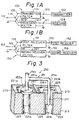
- FIGs. 1A and 1B there are respectively illustrated schematic diagrams of a duplexer 100 and an isolator 150 as two types of isolating circuits.
- the duplexer 100 comprises a transmitter filter 101 having an input terminal 103 and an output terminal 105, and a receiver filter 107 having an input terminal 109 and an output terminal 111.
- the output terminal 105 of the transmitter filter and the input terminal 109 of the receiver filter 107 are commonly coupled to an antenna terminal 113 through a connecting point 115.
- the transmitter filter 101 and receiver filter 107 are respectively supplied with the ground potential.
- the input terminal 103 of the transmitter filter 101, connected to a transmitter 102, and the output terminal 111 of the receiver filter 107, connected to a receiver 108, may be grounded through respective terminal resistors (not shown).
- the duplexer 100 In duplex operation of the transmitter 102 and the receiver 108 connected to a common antenna (not shown), the duplexer 100 is required so as to effectively isolate the transmitter 102 and the receiver 108 to permit simultaneous operation, especially, where the transmitting and receiving frequency signals are closely spaced.
- the transmitter filter 101 of the duplexer 100 is coupled to the transmitting frequency signals in a first frequency range from 824 HMz to 849 HMz and attenuates the other frequency signals in the other frequency range either below 824 MHz or above 849 MHz, while the receiver filter 107 is coupled to the receiving frequency signals in a second frequency range from 869 MHz to 894 HMz and attenuates the other frequency signals either below 869 HMz or above 894 HMz. Therefore, the duplexer 100 transmits the transmitting frequency signals from the transmitter 102 only into the antenna terminal 113 through the transmitter filter 101, and also transmits the receiving frequency signals from the antenna terminal 113 only into the receiver 108 through the receiver filter 107.
- the isolator 150 in Fig. 1B comprises a first receiver filter 151 having an input terminal 153 and an output terminal 155, and a second receiver filter 157 having an input terminal 159 and an output terminal 161.
- the input terminal 153 of the first receiver filter 151 and the input terminal 159 of the second receiver filter 157 are commonly coupled to an antenna terminal 163 through a connecting point 165.
- the first and second receiver filters 151 and 157 are respectively supplied with the ground potential.
- the respective output terminals 155 and 161 of the first and second receiver filters 151 and 157, respectively connected to first and second receiver, may be grounded through respective terminal resistors (not shown).
- the first receiver filter 151 is coupled to the first receiving frequency signals in a first frequency range and attenuates the other frequency signals in the other frequency range, while the second receiver filter 157 is coupled to the second receiving frequency signals in a second frequency range, higher than the first frequency range, and attenuates the other frequency signals. Therefore, the isolator 150 transmits the first receiving frequency signals from the antenna terminal 163 only into the first receiver 152 through the first receiver filter 151, and also transmits the second receiving frequency signals from the antenna terminal 163 only into the second receiver 158 through the second receiver filter 157.
- a first dielectric filter 200 which is applicable to either the transmitter filter 101 in Fig. 1A or the first receiver filter 151 in Fig. 1B.
- the first dielectric filter 200 includes a substantially rectangularly shaped block 210 of ceramic materials, primarily BaO and TiO2.
- the block has a top surface 211, a bottom surface 213, a pair of mutually parallel first side surfaces 215a and 215b and a pair of mutually parallel second side surfaces 217a and 217b.
- the block 210 further has four cylindrical interior surfaces therein which respectively define corresponding holes 219a, 219b, 219c and 219d each extending from the top surface 211 to the bottom surface 213 and arranged in a vertical plane to the first side surface 215a and 215b.
- Each of the interior surfaces in the block 210 is entirely covered with a layer of a conductive material such as silver or copper so as to form inner conductive layers 221a, 221b, 221c and 221d.
- FIG. 3 there is illustrated a partially cross section of the first dielectric filter 200 shown in Fig. 2, substantially taken along lines A-A′.
- the inner conductive layers 221a-221d are electrically connected with one another by means of a bottom conductive layer 223 which may also be formed of silver or copper on the bottom surface 213 of the block 210.
- the bottom conductive layer 223 is electrically connected with similarly formed side conductive layers 225 provided on the side surfaces 215a, 215b, 217a and 217b.
- the first, second, third and fourth resonators 235a, 235b, 235c and 235d have respective top conductive layers 231a, 231b, 231c and 231d, shown in Figs 2 and 3.
- the top conductive layers 231a-231d respectively form collars covering the portions of the top surface 211 surrounding the four holes 219a-219d and are respectively connected to the corresponding inner conductive layers 221a- 221d.
- the block 210 further has first, second and third coupling conductive layers 241, 243 and 245 provided on the top surface 211 thereof.
- the second coupling conductive layer 243 connected to the side conductive layer 225 covering the first side surface 215a and 215b, is spaced from and provided between the top conductive layers 231c and 231d of the third an fourth resonators 235c and 235d in order to adjust the coupling frequencies between the third and fourth resonators 235c and 235d.
- each of the conductive layers 221, 223, 225, 231, 241, 243 and 245 is about 2 microns.
- the first dielectric filter 200 in Fig. 2 further employs first and second coupling terminals 250 and 260.
- the first and second coupling terminals 250 and 260 respectively have first and second "h"-shaped conductive parts 251 and 261 whose arms 251a and 261a respectively form the input and output terminals of either the transmitter filter 101 in Fig. 1A or the first receiver filter 151 in Fig. 1B.
- the first and second coupling terminals 250 and 260 each further includes two bushings 253a, 253b, 263a and 263b, made of dielectric materials such as polypropylene, polycarbonate, epoxy resin or ABC′ resin, and each having a thin round recess 271 therein.
- the legs 251b, 251c, 261b and 261c of the first and second conductive parts 251 and 261 are respectively fitted into the respective recesses 271 of bushings 253a, 253b, 263a and 263b.
- the bushings 253a, 253b, 263a and 263b are respectively fitted into the corresponding holes 219a, 219b, 219c and 219d so that the legs 251b, 251c, 261b and 261c of the first and second conductive parts 251 and 261 are respectively coupled with the corresponding inner conductive layers 221a, 221b, 221c and 221d.
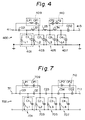
- FIG. 4 there is illustrated an equivalent circuit 400 of the dielectric filter 200 shown in Fig. 2.
- the equivalent circuit 400 has input and output terminals 411 and 413 formed by the respective arms 251a and 261a of the conductive parts 251 and 261 in Fig. 2, and first second, third and fourth resonator circuits 401, 403, 405 and 407 corresponding to the first, second, third and forth resonators 235a, 235b, 235c and 235d.
- Each resonator circuits 401, 403, 405 and 407 respectively formed by respective capacitances C1, C2, C3 and C4 and inductances L1, L2, L3 and L4, coupled to adjacent resonators by means of inductances L12, L23, L34 set up by the respective first, second and third coupling conductive layers 241, 243 and 245.
- the input terminal 411 is coupled to the first resonator circuit 401 through a capacitance C01 set up between the legs 251b of the first conductive part 251 and the inner conductor 221a through the bushing 253a, and further coupled to the second resonator circuit 403 through a inductor Lp1, set up by the first conductive part 251, and a composite capacitance Cp1 which is composed of the capacitance C01 and a capacitance set up between the legs 251c of the first conductive part 251 and the inner conductor 221b through the bushing 253b.
- While the output terminal 413 is coupled to the fourth resonator circuit 407 through a capacitance C02 set up between the legs 261b of the second conductive part 261 and the inner conductor 221d through the bushing 263a, and further coupled to the third resonator circuit 405 through a inductor Lp2, set up by the second conductive part 261, and a composite capacitance Cp2 which is composed of the capacitance C02 and a capacitance set up between the legs 261c of the second conductive part 261 and the inner conductor 221c through the bushing 263b.
- First and second coupling terminal circuits 409 and 410 composed of Cp1, Lp1, Cp2 and Lp2, are set up by the respective first and second coupling terminals 250 and 260.
- the above mentioned circuit 400 has first and second maximum values of the attenuation at first and second maximum attenuated frequency f ⁇ 1 and f ⁇ 2 near the first frequency range, that is, the pass band of the circuit 400 by means of the respective inductances L p 1 and L p 2 and composite capacitances C p 1 and C p 2, respectively set up by the first and second coupling terminal circuits 409 and 410 in Fig. 4.
- the first maximum value of the attenuation against the first maximum attenuated frequency f ⁇ 1 set up by the first coupling terminal circuit 409 can be calculated in the following manner:
- the matrix F composed of the first resonator 401 and the first coupling terminal circuit 409 is expressed by the following matrix (1):
- A B2 + 1 S*C p 1 (1 + C1 C01 + 1 S2*L1*C01 )
- B [L1 + L12 + S2 * L1 * L12 * (C01+C1)] S2 * L1 * C01 + C p 1
- C C1 C01 + L12 L1 + C1 C1 + 1 S2*L1 * ( 1 C01 + 1 C p 1 ) + S2 * L12 * C1
- D B2 + 1 S*C p 1 * (1 + L12 L1 + S2 * L12 * C1)
- B2 [L1 + L12 + S2 * L1 * L12 * (C01 + C1)] S * L12 * C01
- K1 1 S*C p 1 + B2
- the first dielectric filter 200 having the equivalent circuit 400 has at least two maximum values of the attenuation above the center frequency f01 of the first frequency range (the pass band thereof).
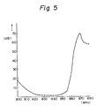
- Fig. 5 there is shown the attenuation volume according to the first dielectric filter 200 shown in Fig. 2 in the frequency range from 800 MHz to 880 MHz.
- the attenuation by the first dielectric filter 200 is significantly low level in the first frequency range from 824 MHz to 849 MHz, that is, the first dielectric filter 200 is coupled to the first signals in the first frequency range.
- the attenuation is increased at a first attenuation rate, while in the fourth frequency range above the first frequency range the attenuation is suddenly increased at a second attenuation rate which is greater than the first attenuation rate by means of the first and second coupling terminals 250 and 260 so as to significantly isolate the second frequency signals, coupled to another filter, in the second frequency range from 869 MHz to 894 MHz.
- a second dielectric filter 600 which is applicable to either the receiver filter 107 in Fig. 1A or the second receiver filter 157 in Fig. 1B.
- the second dielectric filter 600 being alike to the first dielectric filter 200 in Fig. 2 except for first, second and third coupling conductive layer 641, 643 and 645, includes a block 610 of ceramic materials.
- the block 610 has a top surface 611, a bottom surface 613, first side surfaces 615a and 615b, second side surfaces 617a and 617b and, further, tour cylindrical interior surfaces therein which respectively define corresponding holes 619a, 619b, 619c and 619d each extending from the top surface 611 to the bottom surface 613.
- Each of the interior surfaces in the block 610 is entirely covered with a layer or a conductive material such as a silver or copper so as to form inner conductive layers 621a, 621b, 621c and 621d.
- the inner conductive layers 621a-621d are also electrically connected with one another by means of a bottom conductive layer 623 on the bottom surface 613.
- the bottom conductive layer 623 is electrically connected with a side conductive layer 625 provided on the side surfaces 615a, 615b, 617a and 617d.
- the first, second, third and fourth resonators 635a-635d have respective top conductive layers 631a, 631b, 631c and 631d, respectively connected with the corresponding inner conductive layers 621a-621d on the top surface 611.
- the block 610 further has the first, second and third coupling conductive layers 641, 643 and 645 spaced from the provided between the side conductive layer 625 covering the first side surfaces 615a and 615b on the top surface 611 thereof.
- the first coupling conductive layer 641 is spaced from and provided between the top conductive layers 631a and 631b in order to adjust the coupling frequencies between the first and second resonators 635a and 635b.
- the second conductive layer 643 is spaced from and provided between the top conductive layers 231b and 231c of the second and third resonators 635b and 635c in order to adjust the coupling frequencies between the second and third resonators.
- the third coupling conductive layer 645 is also spaced from and provided between the top conductive layers 631c and 631d of the third and fourth resonators 635c and 635d in order to adjust the coupling frequencies between the third and fourth resonators 635c and 635d.
- the second dielectric filter 600 in Fig. 6 further employs first and second coupling terminals 650 and 660.
- the first and second coupling terminals 650 and 660 respectively have first and second "h"-shaped conductive parts 650 and 661 whose arms 651a and 661a respectively form the input and output terminals of either the receiver filter 107 in Fig. 1A or the second receiver filter 157 in Fig. 1B.
- the first and second coupling terminals 650 and 660 each further includes two bushings 653a, 653b, 663a and 663b each having a thin round recess 671 therein.
- the legs 651b, 651c, 661b and 661c of the first and second conductive parts 651 and 661 are respectively fitted into the respective recesses 671 of bushings 653a, 653b, 663a and 663b.
- the bushings 653a, 653b, 663a and 663b are further respectively fitted into the corresponding holes 619a, 619b, 619c and 619d so that the legs 651b, 651c, 661b and 661c of the first and second conductive parts 651 and 661 are respectively coupled with the corresponding inner conductive layers 621a-621d.
- FIG. 7 there is illustrated an equivalent circuit 700 of the second dielectric filter 600 shown in Fig. 6.
- the equivalent circuit 700 has input and output terminals 711 and 713 formed by the respective arms 651a and 661a of the conductive parts 651 and 661 in Fig. 6, and first, second, third and fourth resonator circuits 701, 703, 705 and 707 corresponding to the first, second, third and fourth resonators 635a, 635b, 635c and 635d.
- Each resonator circuits 701, 703, 705 and 707 respectively formed by respective capacitances C1 , C2, C3 and C4 and inductances L1, L2, L3 and L4, coupled to adjacent resonators by means of capacitance C12, C23, C34 set up by the respective first, second and third coupling conductive layers 241, 243 and 245.
- the input terminal 711 is coupled to the first resonator circuit 701 through a capacitance C01 set up between the legs 651b of the first conductive part 651 and the inner conductor 621a through the bushing 653a, and further coupled to the second resonator circuit 403 through a inductor L p 1, set up by the first conductive part 651, and a composite capacitance C p 1 which is composed of the capacitance C01 and a capacitance set up between the legs 651c of the first conductive part 651 and the inner conductor 621b through the bushing 653b.
- While the output terminal 713 is coupled to the fourth resonator circuit 707 through a capacitance C02 set up between the legs 661b of the second conductive part 661 and the inner conductor 621d through the bushing 663a, and further coupled to the third resonator circuit 705 through a inductor L p 2, set up by the second conductive part 661, and a composite capacitance C p 2 which is composed of the capacitance C02 and a capacitance set up between the legs 661c of the second conductive part 661 and the inner conductor 621c through the bushing 663b.
- First and second coupling terminal circuits 709 and 710 composed of L p 1, C p 1, L p 2 and C p 2, is set up by the respective first and second coupling terminals 650 and 660.
- the above mentioned circuit 700 has first and second maximum values of the attenuation near the second frequency range, that is the pass band of the circuit 700 by means of the respective inductances L p 1 and L p 2 and composite capacitances C p 1 and C p 2, respectively set up by the first and second coupling terminal circuits 709 and 710 in Fig. 7.
- the first maximum value of the attenuation set up by the first coupling terminal circuit 709 can be calculated in the following manner:
- the second dielectric filter 600 having the equivalent circuit 700 has at least two maximum values of the attenuation below the center frequency f02 of the second frequency range (the pass band thereof).
- Fig. 8 there is shown the attenuation volume according to the second dielectric filter 600 shown in Fig. 6 in the frequency range from 820 HMz to 900 lfHMz.
- the attenuation by the second dielectric filter 600 is significantly low level in the second frequency range from 863 HMz to 894 HMz, that is, the second dielectric filter 600 is coupled to the second signals in the second frequency range.
- the attenuation is suddenly increased at a third attenuation rate, while in the sixth frequency range above the second frequency range the attenuation is increased at a fourth attenuation rate.
- the third attenuation rate is greater than the fourth attenuation rate by means of the first and second coupling terminals 650 and 660 so as to significantly isolate the first frequency signals, coupled to the first dielectric filter, in the first frequency range from 824 MHz to 849 HMz.
- both of the first and second dielectric filter 200 and 600 can respectively have at least one maximum value of attenuation in the range above the first frequency range and below the second frequency range if each of the first and second dielectric filter 200 and 600 has at least one coupling terminals which couples either the first resonator to the second (adjacent) resonator or the fourth (final) resonator to the third (adjacent) resonator.
- the isolating circuit, composed of such first and second dielectric filter should sufficiently isolate the first and second frequency signals.
Landscapes
- Physics & Mathematics (AREA)
- Electromagnetism (AREA)
- Control Of Motors That Do Not Use Commutators (AREA)
Description
- The present disclosure relates to the subject matter disclosed in Japanese Patent Application Nos. 63-150136 filed on June 20th, 1988 and 63-218475 filed on September 2nd, 1988.
- The present invention relates to an isolating circuit and a pair of dielectric filters for use therein, more particularly an isolating circuit, such as a duplexer or an isolator, for isolating a first frquency signal in a first frequency range and a second frequency signal is a second frequency range which is higher than the first frequency range, and still more particularly a duplexer well adapted for a mobile telephone.
- The demand for services of the mobile telephone in large cities such as New York, London, Tokyo etc. has suddenly been expanded more than the initiate estimation thereof and, therefore, has caused a shortage of the number of channels for communication services. In order to solve this shortage, there are mobile telephone service corporations planning or having carried out a channel number increase, for example, from 666 channels to 832 channels in the U. S. and from 600 channels to 1320 channels in the U.K., as described in the Publication, Tomokazu Komazaki et al. "Dielectric Filter with Attenuation Pole for Mobile Radio", Electron Information Communication Society, CAS88-10, dated on June 23rd, 1988.
- In accordance with the channel number increase, it is necessary to extend the bandwidth for radio communications. In the U. S., the transmitting frequency band and receiving frequency band have respectively extended from 825-845 MHz to 824-849 MHz and from 870-890 MHz to 869-894MHz. As a consequence, a duplexer is required so as to more effectively isolate the transmitter and the receiver to permit simultaneous operation since the transmitting and receiving frequencies are more closely spaced. The dielectric filters which may be used in such duplexer are disclosed in Japanese laid-open patent publication Nos. 62-77703 (published on April 9th, 1987) and 62-157402 (published on July 13th, 1987).
- A dielectric filter, disclosed in Japanese laid-open patent publication No. 62-77703, has six dielectric resonators therein and a reactance circuit formed by a capacitor or a inductor. The reactance circuit, jumping over at least one resonator, connect two resonators out of the remaining resonators of the dielectric filter. As a result the dielectric filters each have an attenuation pole.
- A dielectric filter, disclosed in Japanese laid-open patent publication No. 62-157402, has four dielectric resonators therein and a coaxial cable having two edge portions. The coaxial cable, jumping over two resonators, couple the two remaining resonators of the dielectric filter through two reactance components, respectively connected to two edge portions thereof. As a result the dielectric filters have two attenuation poles which are asymnetric relative to the center frequency.
- Another dielectric filter is disclosed in Japanese laid-open patent JP-A-62239701 which relates to a method and a device for phase adjustment of a dielectric filter. The disclosed device comprises a dielectric block having three trough-holes forming a three-stage dielectric filter and an additional through-hole which allows for phase adjustment of the filter. The phase-adjustment hole and the filter are interconnected by a h-shaped conductive part.
- A further radio frequency filter is known from GB-
A-2 165 098 which comprises a ceramic filter block covered with conductive material and includes two holes beeing surrounded by capacitive strips. The signal is input and output via electrodes being isolated from ground. -
- It is an object of the present invention to provide an improved isolating circuit composed of at least two different types of filters, more secifically, the combination of the two different types of filters in order to more effectively seperate a first frequency signal in a first frequency range and a second frequency signal in a second frequency range which is higher than the first frequency range. This object is achieved with an isolating circuit according to claim 1.
- It is another object of the present invention to provide an improved dielectric filter for use in the above mentioned isolating circuit. This object is achieved with a dielectric filter according to claim 5.
- In accordance with this invention, it is relatively easy to design an isolation circuit which meet the strict restriction of isolating the first and second frequency signals more closely spaced as discussed in the column of BACKGROUND OF THE INVENTION since it is only required to partly change each of the attenuation frequency character of the first and second filter.
- In accordance with another aspect of the invention, a dielectric filter includes a dielectric block having top, bottom, side surfaces and further a plurality of interior surfaces difining respective holes each extending from the top to bottom surfaces thereof. The filter has a side conductive layer covering the side surface, a bottom conductive layer covering said bottom surface electrically connected to the side layer, and first, second, third and fourth inner conductive layers respectively covering the interior surfaces and electrically connected to the bottom layer. The second inner layer is provided between the first and third inner layers and next to the first inner layer. The third inner layer is provided between the second and fourth inner layers and next to the fourth inner layer. The filter further has a first coupling terminal inductively and capacitively couples the first inner layer to the second inner layer.
- These and other features and advantages of the invention will be more completely understood from the following detailed description of the preferred embodiments with reference to the accompany drawings in which:
- Figs. 1A and 1B are respectively schematic diagrams of a
duplexer 100 and anisolator 150; - Fig. 2 is a perspective view of a first dielectric filter 200;
- Fig. 3 is a partial cross section of the first dielectric filter 200 shown in Fig. 2, taken along lines A-A′;
- Fig. 4 is a schematic equivalent circuit of the first dielectric filter 200;
- Fig. 5 is a graph illustrating the attenuation frequency character of the
second filter 600; - Fig. 6 is a perspective view of a second
dielectric filter 600; - Fig. 7 is a schematic equivalent circuit of the second
dielectric filter 600; and - Fig. 8 is a graph illustrating the attenuation frequency character of the second
dielectric filter 600. - Referring to Figs. 1A and 1B, there are respectively illustrated schematic diagrams of a
duplexer 100 and anisolator 150 as two types of isolating circuits. - The
duplexer 100 comprises atransmitter filter 101 having aninput terminal 103 and anoutput terminal 105, and areceiver filter 107 having aninput terminal 109 and anoutput terminal 111. Theoutput terminal 105 of the transmitter filter and theinput terminal 109 of thereceiver filter 107 are commonly coupled to anantenna terminal 113 through aconnecting point 115. Thetransmitter filter 101 andreceiver filter 107 are respectively supplied with the ground potential. Theinput terminal 103 of thetransmitter filter 101, connected to atransmitter 102, and theoutput terminal 111 of thereceiver filter 107, connected to areceiver 108, may be grounded through respective terminal resistors (not shown). - In duplex operation of the
transmitter 102 and thereceiver 108 connected to a common antenna (not shown), theduplexer 100 is required so as to effectively isolate thetransmitter 102 and thereceiver 108 to permit simultaneous operation, especially, where the transmitting and receiving frequency signals are closely spaced. Thetransmitter filter 101 of theduplexer 100 is coupled to the transmitting frequency signals in a first frequency range from 824 HMz to 849 HMz and attenuates the other frequency signals in the other frequency range either below 824 MHz or above 849 MHz, while thereceiver filter 107 is coupled to the receiving frequency signals in a second frequency range from 869 MHz to 894 HMz and attenuates the other frequency signals either below 869 HMz or above 894 HMz. Therefore, theduplexer 100 transmits the transmitting frequency signals from thetransmitter 102 only into theantenna terminal 113 through thetransmitter filter 101, and also transmits the receiving frequency signals from theantenna terminal 113 only into thereceiver 108 through thereceiver filter 107. - Meanwhile, the
isolator 150 in Fig. 1B comprises afirst receiver filter 151 having aninput terminal 153 and anoutput terminal 155, and asecond receiver filter 157 having aninput terminal 159 and anoutput terminal 161. Theinput terminal 153 of thefirst receiver filter 151 and theinput terminal 159 of thesecond receiver filter 157 are commonly coupled to anantenna terminal 163 through aconnecting point 165. The first andsecond receiver filters respective output terminals second receiver filters first receiver filter 151 is coupled to the first receiving frequency signals in a first frequency range and attenuates the other frequency signals in the other frequency range, while thesecond receiver filter 157 is coupled to the second receiving frequency signals in a second frequency range, higher than the first frequency range, and attenuates the other frequency signals. Therefore, theisolator 150 transmits the first receiving frequency signals from theantenna terminal 163 only into thefirst receiver 152 through thefirst receiver filter 151, and also transmits the second receiving frequency signals from theantenna terminal 163 only into thesecond receiver 158 through thesecond receiver filter 157. - As to the preferable connection among the antenna terminal and filters in Figs. 1A and 1B, there is disclosed in more detail in co-owned pending application of serial number 7-237673, filed on August 26th, 1988.
- Referring to Fig. 2, there is illustrated a first dielectric filter 200 which is applicable to either the
transmitter filter 101 in Fig. 1A or thefirst receiver filter 151 in Fig. 1B. - The first dielectric filter 200 includes a substantially rectangularly shaped
block 210 of ceramic materials, primarily BaO and TiO₂. The block has atop surface 211, abottom surface 213, a pair of mutually parallelfirst side surfaces 215a and 215b and a pair of mutually parallelsecond side surfaces block 210 further has four cylindrical interior surfaces therein which respectively define correspondingholes top surface 211 to thebottom surface 213 and arranged in a vertical plane to thefirst side surface 215a and 215b. Each of the interior surfaces in theblock 210 is entirely covered with a layer of a conductive material such as silver or copper so as to form innerconductive layers - Referring to Fig. 3, there is illustrated a partially cross section of the first dielectric filter 200 shown in Fig. 2, substantially taken along lines A-A′.
- The inner
conductive layers 221a-221d are electrically connected with one another by means of a bottomconductive layer 223 which may also be formed of silver or copper on thebottom surface 213 of theblock 210. The bottomconductive layer 223 is electrically connected with similarly formed sideconductive layers 225 provided on theside surfaces - The four inner
conductive layers 221a-221d, surrounded by the dielectric material enclosed in the side and bottom conductive layer, respectively act as first, second, third and fourthdielectric resonator - The first, second, third and
fourth resonators conductive layers conductive layers 231a-231d respectively form collars covering the portions of thetop surface 211 surrounding the four holes 219a-219d and are respectively connected to the corresponding innerconductive layers 221a- 221d. - The
block 210 further has first, second and third couplingconductive layers top surface 211 thereof. The first couplingconductive layer 241, connected to the sideconductive layer 225 covering thefirst side surfaces 215a and 215b, is spaced from and provided between the topconductive layers second resonator second resonators conductive layer 243, connected to the sideconductive layer 225 covering thefirst side surface 215a and 215b, is spaced from and provided between the topconductive layers fourth resonators fourth resonators conductive layer 245, which is extended from the first side surface 215a to the middle portion of the top surface and connected to the sideconductive layer 225 covering the first side surface 215a, is spaced from and provided between the topconductive layers third resonators - The thickness of each of the
conductive layers - The above mentioned structure of the dielectric filter 200 is disclosed in more detail in co-owned pending application of serial number 7-227874, filed on August 3rd, 1988.
- The first dielectric filter 200 in Fig. 2 further employs first and
second coupling terminals second coupling terminals conductive parts arms transmitter filter 101 in Fig. 1A or thefirst receiver filter 151 in Fig. 1B. The first andsecond coupling terminals bushings thin round recess 271 therein. Thelegs conductive parts respective recesses 271 ofbushings bushings holes legs conductive parts conductive layers - Referring to Fig. 4, there is illustrated an
equivalent circuit 400 of the dielectric filter 200 shown in Fig. 2. - The
equivalent circuit 400 has input andoutput terminals 411 and 413 formed by therespective arms conductive parts fourth resonator circuits resonators resonator circuits conductive layers first resonator circuit 401 through a capacitance C01 set up between the legs 251b of the firstconductive part 251 and theinner conductor 221a through the bushing 253a, and further coupled to thesecond resonator circuit 403 through a inductor Lp1, set up by the firstconductive part 251, and a composite capacitance Cp1 which is composed of the capacitance C01 and a capacitance set up between thelegs 251c of the firstconductive part 251 and theinner conductor 221b through thebushing 253b. While theoutput terminal 413 is coupled to thefourth resonator circuit 407 through a capacitance C02 set up between thelegs 261b of the secondconductive part 261 and theinner conductor 221d through thebushing 263a, and further coupled to thethird resonator circuit 405 through a inductor Lp2, set up by the secondconductive part 261, and a composite capacitance Cp2 which is composed of the capacitance C02 and a capacitance set up between thelegs 261c of the secondconductive part 261 and the inner conductor 221c through thebushing 263b. First and secondcoupling terminal circuits second coupling terminals - The above mentioned
circuit 400 has first and second maximum values of the attenuation at first and second maximum attenuated frequency f ∞ ₁ and f ∞ ₂ near the first frequency range, that is, the pass band of thecircuit 400 by means of the respective inductances Lp1 andL p2 and composite capacitances Cp1 andC p2, respectively set up by the first and secondcoupling terminal circuits - The first maximum value of the attenuation against the first maximum attenuated frequency f∞₁ set up by the first
coupling terminal circuit 409 can be calculated in the following manner: - The matrix F composed of the
first resonator 401 and the firstcoupling terminal circuit 409 is expressed by the following matrix (1):
Wherein


s = j*ωx (j is an imaginary unit, ω x = 2πfx, fx is a frequency), and
herein the value of L₁ of the firstcoupling terminal circuit 409 is ignored since generally | Lp1 | << | 1/ωCp1 | , that is, the impedance of the capacitance Cp1 is significantly larger than that of the inductance Lp₁. - Since the frequency fx of the above matrix (1) is the first maximum attenuated frequency f ∞₁ at the time of K1=0, according to the matrix (1) the first maximum attenuated frequency f ∞ ₁(=ω ₁/2π) can be expressed by the following equation (2):


Meanwhile, the center frequency f₀₁ (= ω 01/2 π) of the first frequency range of the above mentionedcircuit 400 can be expressed by the following equiation (4):
Therefore, the equations (3) and (4) show f ∞ ₁ > f₀₁ since µ∞1 > ω₀₁. Similarly the second maximum value of the attenuation against the second maximum attenuated frequency f ∞ ₂ can be calculated and will be found that f ∞ ₂ > f₀₁. - As a consequence of the foregoing calculation, the first dielectric filter 200 having the
equivalent circuit 400 has at least two maximum values of the attenuation above the center frequency f₀₁ of the first frequency range (the pass band thereof). - Now referring to Fig. 5, there is shown the attenuation volume according to the first dielectric filter 200 shown in Fig. 2 in the frequency range from 800 MHz to 880 MHz.
- As shown in Fig. 5, the attenuation by the first dielectric filter 200 is significantly low level in the first frequency range from 824 MHz to 849 MHz, that is, the first dielectric filter 200 is coupled to the first signals in the first frequency range. In a third frequency range below the first frequency range, the attenuation is increased at a first attenuation rate, while in the fourth frequency range above the first frequency range the attenuation is suddenly increased at a second attenuation rate which is greater than the first attenuation rate by means of the first and
second coupling terminals - Referring to Fig. 6, there is illustrated a second
dielectric filter 600 which is applicable to either thereceiver filter 107 in Fig. 1A or thesecond receiver filter 157 in Fig. 1B. - The second
dielectric filter 600, being alike to the first dielectric filter 200 in Fig. 2 except for first, second and third couplingconductive layer block 610 of ceramic materials. Theblock 610 has atop surface 611, abottom surface 613,first side surfaces second side surfaces holes top surface 611 to thebottom surface 613. Each of the interior surfaces in theblock 610 is entirely covered with a layer or a conductive material such as a silver or copper so as to form innerconductive layers - The inner
conductive layers 621a-621d are also electrically connected with one another by means of a bottomconductive layer 623 on thebottom surface 613. The bottomconductive layer 623 is electrically connected with a sideconductive layer 625 provided on theside surfaces - The four inner
conductive layers 621a-621d, surrounded by the dielectric material enclosed in the side and bottomconductive layers fourth resonators - The first, second, third and
fourth resonators 635a-635d have respective topconductive layers conductive layers 621a-621d on thetop surface 611. - The
block 610 further has the first, second and third couplingconductive layers conductive layer 625 covering thefirst side surfaces top surface 611 thereof. The first couplingconductive layer 641 is spaced from and provided between the topconductive layers second resonators conductive layer 643 is spaced from and provided between the topconductive layers third resonators conductive layer 645 is also spaced from and provided between the topconductive layers fourth resonators fourth resonators - The second
dielectric filter 600 in Fig. 6 further employs first andsecond coupling terminals second coupling terminals conductive parts arms 651a and 661a respectively form the input and output terminals of either thereceiver filter 107 in Fig. 1A or thesecond receiver filter 157 in Fig. 1B. The first andsecond coupling terminals bushings thin round recess 671 therein. Thelegs conductive parts respective recesses 671 ofbushings bushings holes legs conductive parts conductive layers 621a-621d. - Referring to Fig. 7, there is illustrated an
equivalent circuit 700 of the seconddielectric filter 600 shown in Fig. 6. - The
equivalent circuit 700 has input andoutput terminals respective arms 651a and 661a of theconductive parts fourth resonator circuits fourth resonators resonator circuits conductive layers input terminal 711 is coupled to thefirst resonator circuit 701 through a capacitance C01 set up between thelegs 651b of the firstconductive part 651 and theinner conductor 621a through thebushing 653a, and further coupled to thesecond resonator circuit 403 through a inductor Lp1, set up by the firstconductive part 651, and a composite capacitance Cp1 which is composed of the capacitance C01 and a capacitance set up between thelegs 651c of the firstconductive part 651 and theinner conductor 621b through thebushing 653b. While theoutput terminal 713 is coupled to thefourth resonator circuit 707 through a capacitance C02 set up between thelegs 661b of the secondconductive part 661 and the inner conductor 621d through thebushing 663a, and further coupled to thethird resonator circuit 705 through ainductor L p2, set up by the secondconductive part 661, and acomposite capacitance C p2 which is composed of the capacitance C02 and a capacitance set up between thelegs 661c of the secondconductive part 661 and theinner conductor 621c through thebushing 663b. First and secondcoupling terminal circuits L p2 andC p2, is set up by the respective first andsecond coupling terminals - The above mentioned
circuit 700 has first and second maximum values of the attenuation near the second frequency range, that is the pass band of thecircuit 700 by means of the respective inductances Lp1 andL p2 and composite capacitances Cp1 andC p2, respectively set up by the first and secondcoupling terminal circuits - The first maximum value of the attenuation set up by the first
coupling terminal circuit 709 can be calculated in the following manner: - The matrix F composed of the
first resonator 701 and the firstcoupling terminal circuit 709 is expressed by the following matrix (5):
wherein


s = j*ωx (j is an imaginary unit, ω x = 2πfx, fx is a frequency), and
herein the value of Lp1 of the firstcoupling terminal circuit 709 is ignored since generally | Lp1 | << | 1/ωCp1 | , that is, the impedance of the capacitance Cp1 is significantly larger than that of the inductance Lp1. - Since the frequency fx of the above matrix (5) is the first maximum attenuated frequency f ∞ ₁ at the time of K2=0, according to the matrix (5) the first maximum attenuated frequency f ∞ ₁ (=ω∞₁/2π) can be expressed by the following equation (6):

Meanwhile, the center frequency f₀₂ (=ω₀₂/2π) of the second frequency range of the above mentionedcircuit 700 can be expressed by the following equation (7):
Therefore, the equations (6) and (7) show f ∞ ₁ < f₀₁ since 1/ω∞1 > 1/ω∞01. Similarly the second maximum value of the attenuation against the second maximum attenuated frequency f ∞ ₂ can be calculated and will be found that f ∞ ₂ < f₀₂. - As a consequence of the foregoing calculation, the second
dielectric filter 600 having theequivalent circuit 700 has at least two maximum values of the attenuation below the center frequency f₀₂ of the second frequency range (the pass band thereof). - Now referring to Fig. 8, there is shown the attenuation volume according to the second
dielectric filter 600 shown in Fig. 6 in the frequency range from 820 HMz to 900 lfHMz. - As shown in Fig. 8, the attenuation by the second
dielectric filter 600 is significantly low level in the second frequency range from 863 HMz to 894 HMz, that is, the seconddielectric filter 600 is coupled to the second signals in the second frequency range. In a fifth frequency range below the second frequency range, the attenuation is suddenly increased at a third attenuation rate, while in the sixth frequency range above the second frequency range the attenuation is increased at a fourth attenuation rate. The third attenuation rate is greater than the fourth attenuation rate by means of the first andsecond coupling terminals - For example, both of the first and second
dielectric filter 200 and 600 can respectively have at least one maximum value of attenuation in the range above the first frequency range and below the second frequency range if each of the first and seconddielectric filter 200 and 600 has at least one coupling terminals which couples either the first resonator to the second (adjacent) resonator or the fourth (final) resonator to the third (adjacent) resonator. As a consequence, the isolating circuit, composed of such first and second dielectric filter should sufficiently isolate the first and second frequency signals.
Claims (10)
- Isolating circuit (100) for separating a first frequency signal in a first frequency range and a second frequency signal in a second frequency range, said isolating circuit comprising:- a first filter (101, 200) for separating said first frequency signal, said first filter having a first input terminal (103, 250) and a first output terminal (105, 260) for being coupled to first input signal including the first frequency signal at said first input terminal and for attenuating first frequency components of the first input signal below the first frequency range at a first attenuation rate and second frequency components of the first input signal above the first frequency range at a second attenuation rate,- two first conductive parts (251, 261), said first conductive parts are used for setting the first and second attenuation rate so that the second attenuation rate is greater than the first attenuation rate, and- elements forming a plurality of first resonators (235a-235d), wherein two (235a, 235b) of said first resonators are coupled to said first input terminal (103, 250) via a first one (251) of said conductive parts (251, 261), wherein two others (235c, 235d) of said first resonators are coupled to said first output terminal (105, 260) via a second one (261) of said first conductive parts (251, 261), characterized in that
each said two first conductive parts (251, 261) include a respective first leg (251b, 261b) and a respective second leg (251c, 261c) forming impedances (C01, Cp1+Lp1; C02, Cp2+Lp2) coupling the first input and output terminal to the respective first resonators,- a second filter (107, 600) for separating said second frequency signal,- said second filter having a second input terminal (109, 650) and a second output terminal (111, 660) for being coupled to second input signal including the second frequency signal at said second input terminal and for attenuating third frequency components of the second input signal below the second frequency range at a third attenuation rate and fourth frequency components of the second input signal above the first frequency range at a fourth attenuation rate,
two second conductive parts (651, 661), said second conductive parts are used for setting the third and fourth attenuation rate so that the third attenuation rate is greater than the fourth attenuation rate, and- elements forming a plurality of second resonators (635a-635d), wherein two (635a, 635b) of said second resonators are coupled to said second input terminal (109, 650) via a first one (651) of said second conductive parts (651, 661), wherein two others (635c, 635d) of said first resonators are coupled to said second output terminal (111, 660), via a second one (661) of said second conductive parts (651, 661) and wherein each said two second conductive parts (651, 661) include a respective third leg (651b, 661b) and a respective fourth leg (651c, 661c) forming impedances (C01, Cp1+Lp1; C02, Cp2+Lp2) coupling the second input and output terminal to the respective second resonators;- an antenna terminal (113) coupled to one of the first input and output terminals of the first filter and one of the second input and output terminals of the second filter. - Isolating circuit according to claim 1,
wherein said first filter (101, 200) further comprises at least one first insulating bushing (253a, 253b) having a recess (271) and at least one second insulating bushing (263a, 263b) having a recess (271);
wherein said elements forming a plurality of first resonators (235a-235d) includes
a first dielectric block (210) having a top surface (211), a bottom surface (213), and side surfaces (215,217), said first dielectric block further having interior surfaces defining holes (219a-219d) extending from the top surface to the bottom surface,
a side conductive layer (225) covering said side surfaces (215,217),
a bottom conductive layer (223) covering the bottom surface (213) and electrically connected to said side conductive layer (225), and
inner conductive layers (221a-221d) covering said interior surfaces, said inner conductive layers being electrically connected to said bottom conductive layer (223) and spaced from said side layer (225) at said top surface (211), and
wherein said first and second legs (251b, 251c, 261b, 261c) of each said two first conductive parts (251, 261) are inserted into recess (271) of respective first and second insulating bushings (253a, 253b, 263a, 263b) which are disposed in respective first resonators (235a-235d) of said first filter. - Isolating circuit according to claim 2,
wherein said second filter further (107, 600) comprises at least one third insulating bushing (653a, 653b) having a recess and at least one fourth insulating bushing (663a, 663b) having a recess;
wherein said elements for forming a plurality of second resonators (635a-635d) includes
a second dielectric block (610) having a top surface (611), a bottom surface; and side surface (615,617), said second dielectric block further having interior surfaces defining holes (619a-619d) extending from the top surface to the bottom surface of said second dielectric block, a side conductive layer (665) covering said side surfaces (615,627) of said second dielectric block,
a bottom conductive layer (623) covering the bottom surface (613) of said second dielectric block and electrically connected to said side conductive layer on said second dielectric block, and
inner conductive layers (621a-621d) covering said interior surfaces of said second dielectric block, said inner conductive layers being electrically connected to said bottom conductive layer (623) on said second dielectric block and spaced from said side layer (625) on said second dielectric block at said top surface (611) of said second dielectric block; and
wherein said third and fourth legs (651b, 651c, 661b, 661c) of each said two first conductive parts (651, 661) are inserted into recess (671) of respective third and fourth insulating bushings (653a, 653b, 663a, 663b) which are disposed in respective second resonators (635a-635d) of said second filter. - Isolating circuit according to claim 3,
wherein said first filter further has at least one first coupling layer (241, 243, 245) on said top surface (211) of said first dielectric block and electrically connected to said side conductive layer (225) on said first dielectric block,
said at least one first coupling layer being spaced from and provided between each two first resonators (235) coupled by said two first conductive parts (251, 261); and
wherein said second filter further has at least one second coupling layer (641,643,645) on said top surface (211) of said second dielectric block, said at least one second coupling layer being spaced from and provided between each two second resonators (635) coupled by said two second conductive parts (651, 661). - Dielectric filter (200, 600) comprising:
a dielectric block (210, 610) having a top surface (211, 611), a bottom surface (213, 613), and side surfaces (215a, 215b, 217a, 217b, 615a, 615b, 617a, 617b), said dielectric block further having four interior surfaces defining respective holes (219a-219d,619a-619d) extending from the top surface to the bottom surface;
a side conductive layer (225, 625) covering said side surfaces (215a, 215b, 217a, 217b, 615a, 615b, 617a, 617b);
a bottom conductive layer (223, 623) covering said bottom surface (213, 613) and electrically connected to said side conductive layer (225, 625);
four innner conductive layers (221a-221d, 621a-621d) covering said interior surfaces;
input means (250, 650) for introducing a signal which is to be filtered by said dielectric filter, said input means (250, 650) including a conductive part (251, 651) having first and second legs (251b, 251c, 651b, 651c), output means (260, 660) for extracting the filtered signal from said dielectric filter, said output means (260, 660) including another conductive part (261, 661) with first and second legs (261b, 261c, 661b, 661c),
characterized in that
coupling layers (241,243,245, 641,643,645) are provided on said top surface of said dielectric block, each coupling layer being spaced and provided between two holes (219a-219d, 619a-619d);
said inner conductive layers being electrically connected to said bottom conductive layer (223, 623) and spaced from said side layer (225, 625) at said top surface (211, 611);
said first leg (251b, 651b) of said conductive part (251, 651) being capacitively coupled to one of said inner conductive layers (221a-221d, 621a-621d) and said second leg (251c, 651c) of said conductive part (251, 651) being capacitively coupled to an adjacent inner conductive layer; and
said first leg (261b, 661b) of said another conductive part (261, 661) being capacitively coupled to a further one of said inner conductive layers (221a-221d, 621a-621d) and said second leg (261c, 661c) of said another conductive part (261, 661) being capacitively coupled to an inner conductive layer which is adjacent said further one of said inner conductive layers (221a-221d, 621a-621d). - Dielectric filter according to claim 5, wherein said input means (250, 650) further includes a first insulating bushing (253a, 653a) having a recess (271, 671) and a second insulating bushing (253b, 653b) having a recess (271, 671), and wherein said first and second legs (251b, 251c, 651b, 651c) of said conductive part (251, 651) of said input means (250, 650) are inserted into said recess (271, 671) of said first and second insulating bushings (253a, 253b, 653a, 653b) which are disposed in respective holes (219a-219d, 619a-619d).
- Dielectric filter according to claim 5 or 6, wherein said coupling layers (241,243,245) are electrically connected to said side conductive layer (225).
- Dielectric filter according to claim 7, wherein said one (245) of said coupling layers (241,243,245) extends from the side surface (215a) to the middle portion of the top surface (211).
- Dielectric filter according to any of the claims 5 - 8, wherein said first and second legs (251b, 251c, 651b, 651c) of said conductive part (250, 650) are parallel legs and wherein said first and second legs (261b, 261c, 661b, 661c) of said another conductive part (261, 661) are parallel legs.
- Dielectric filter according to any of the claims 5 - 9, wherein said holes (219a-219d, 619a-619d) are disposed in a row, the first leg (251b, 651b) of the conductive part (251, 651) being coupled to the inner conductive layer (221a, 621a) covering the interior surface of the hole (219a, 619a) at one end of the row and the first leg (261b, 661b) of the another conductive part (261, 661) being coupled to the inner conductive layer (221d, 621d) covering the interior surface of the hole (219d, 619d) at the other end of the row.
Applications Claiming Priority (4)
| Application Number | Priority Date | Filing Date | Title |
|---|---|---|---|
| JP150136/88 | 1988-06-20 | ||
| JP15013688A JPH01318401A (en) | 1988-06-20 | 1988-06-20 | Polarized dielectric filter |
| JP218475/88 | 1988-09-02 | ||
| JP21847588A JPH0267801A (en) | 1988-09-02 | 1988-09-02 | Polarized dielectric filter |
Publications (3)
| Publication Number | Publication Date |
|---|---|
| EP0347774A2 EP0347774A2 (en) | 1989-12-27 |
| EP0347774A3 EP0347774A3 (en) | 1990-11-22 |
| EP0347774B1 true EP0347774B1 (en) | 1995-11-22 |
Family
ID=26479833
Family Applications (1)
| Application Number | Title | Priority Date | Filing Date |
|---|---|---|---|
| EP89110987A Expired - Lifetime EP0347774B1 (en) | 1988-06-20 | 1989-06-16 | An isolating circuit and dielectric filter for use therein |
Country Status (3)
| Country | Link |
|---|---|
| US (1) | US5015974A (en) |
| EP (1) | EP0347774B1 (en) |
| DE (1) | DE68924873T2 (en) |
Families Citing this family (8)
| Publication number | Priority date | Publication date | Assignee | Title |
|---|---|---|---|---|
| US5227747A (en) * | 1989-06-15 | 1993-07-13 | Oki Electric Industry Co., Ltd. | Dielectric filter having coupling amount adjusting patterns |
| JPH03236603A (en) * | 1990-02-14 | 1991-10-22 | Oki Electric Ind Co Ltd | Dielectric filter |
| US5229729A (en) * | 1989-12-14 | 1993-07-20 | Murata Manufacturing Co., Ltd. | Radio frequency signal combining/sorting apparatus |
| FI88441C (en) * | 1991-06-25 | 1993-05-10 | Lk Products Oy | TEMPERATURKOMPENSERAT DIELEKTRISKT FILTER |
| JP2000174503A (en) * | 1998-12-10 | 2000-06-23 | Ngk Spark Plug Co Ltd | Dielectric filter and method for adjusting frequency bandwidth of the filter |
| US7903679B1 (en) * | 2006-04-11 | 2011-03-08 | Altera Corporation | Power supply filtering for programmable logic device having heterogeneous serial interface architecture |
| CN109845027A (en) | 2016-09-23 | 2019-06-04 | Cts公司 | Ceramic RF filter with the structure for stopping RF signal to couple |
| WO2021258043A1 (en) | 2020-06-18 | 2021-12-23 | Ideal Industries, Inc. | Conductor terminal |
Family Cites Families (17)
| Publication number | Priority date | Publication date | Assignee | Title |
|---|---|---|---|---|
| JPS5657302A (en) * | 1979-10-15 | 1981-05-19 | Murata Mfg Co Ltd | Microwave device using coaxial resonator |
| JPS5679502A (en) * | 1979-11-30 | 1981-06-30 | Matsushita Electric Ind Co Ltd | Band block filter and antenna duplexer |
| JPS60114004A (en) * | 1983-11-25 | 1985-06-20 | Murata Mfg Co Ltd | Dielectric coaxial resonator |
| US4742562A (en) * | 1984-09-27 | 1988-05-03 | Motorola, Inc. | Single-block dual-passband ceramic filter useable with a transceiver |
| GB2165098B (en) * | 1984-09-27 | 1988-05-25 | Motorola Inc | Radio frequency filters |
| US4768003A (en) * | 1984-09-28 | 1988-08-30 | Oki Electric Industry Co., Inc. | Microwave filter |
| JPS61214625A (en) * | 1985-03-19 | 1986-09-24 | Tokyo Electric Co Ltd | antenna coupling circuit |
| JPS6218801A (en) * | 1985-07-17 | 1987-01-27 | Murata Mfg Co Ltd | Dielectric filter |
| JPS62157402A (en) * | 1985-12-27 | 1987-07-13 | Murata Mfg Co Ltd | Dielectric filter |
| JPS6277703A (en) * | 1985-09-30 | 1987-04-09 | Murata Mfg Co Ltd | Dielectric filter |
| US4740765A (en) * | 1985-09-30 | 1988-04-26 | Murata Manufacturing Co., Ltd. | Dielectric filter |
| JPH0793522B2 (en) * | 1986-04-12 | 1995-10-09 | ティーディーケイ株式会社 | Phase adjuster for dielectric filter |
| JPS63961A (en) * | 1986-06-18 | 1988-01-05 | Matsushita Electric Ind Co Ltd | Organic electrolyte cell |
| US4692726A (en) * | 1986-07-25 | 1987-09-08 | Motorola, Inc. | Multiple resonator dielectric filter |
| JPS6342201A (en) * | 1986-08-07 | 1988-02-23 | Alps Electric Co Ltd | Microwave branching filter |
| JPS63124601A (en) * | 1986-11-14 | 1988-05-28 | Oki Electric Ind Co Ltd | Dielectric filter |
| JPS63174402A (en) * | 1987-01-13 | 1988-07-18 | Murata Mfg Co Ltd | Dielectric filter device |
-
1989
- 1989-06-15 US US07/366,516 patent/US5015974A/en not_active Expired - Fee Related
- 1989-06-16 EP EP89110987A patent/EP0347774B1/en not_active Expired - Lifetime
- 1989-06-16 DE DE68924873T patent/DE68924873T2/en not_active Expired - Fee Related
Non-Patent Citations (1)
| Title |
|---|
| & JP-A- 62 198201 (TDK CORP.) 01 September 1987, * |
Also Published As
| Publication number | Publication date |
|---|---|
| US5015974A (en) | 1991-05-14 |
| DE68924873T2 (en) | 1996-05-02 |
| DE68924873D1 (en) | 1996-01-04 |
| EP0347774A3 (en) | 1990-11-22 |
| EP0347774A2 (en) | 1989-12-27 |
Similar Documents
| Publication | Publication Date | Title |
|---|---|---|
| US7116188B2 (en) | Laminated dielectric filter, and antenna duplexer and communication equipment using the same | |
| US6542050B1 (en) | Transmitter-receiver | |
| EP0506340A2 (en) | A dielectric filter | |
| US6222426B1 (en) | Branching filter with a composite circuit of an LC circuit and a serial arm saw resonator | |
| CA2116375A1 (en) | Radio frequency filter | |
| US20030043759A1 (en) | LC filter circuit, laminated LC composite component, multiplexer, and radio communication device | |
| US5686873A (en) | Antenna duplexer having transmit and receive portion formed in a single dielectric block | |
| US5015973A (en) | Duplexer with an isolating circuit on a dielectric plate | |
| EP0347774B1 (en) | An isolating circuit and dielectric filter for use therein | |
| US5486799A (en) | Strip line filter and duplexer filter using the same | |
| US20020135438A1 (en) | Filter unit and duplexer comprising such filter units | |
| US6989725B2 (en) | Dielectric resonator, dielectric filter, dielectric duplexer, and communication apparatus incorporating the same | |
| JPH08191230A (en) | Duplexer | |
| US5712604A (en) | Dielectric filter including at least one band elimination filter | |
| US6008707A (en) | Antenna duplexer | |
| US7183878B2 (en) | Surface acoustic wave filter | |
| CN100426587C (en) | Dielectric substance resonance device, dielectric filter and dielectric duplexer | |
| US6504452B2 (en) | Low-pass filter and mobile communication device using the same | |
| KR100449226B1 (en) | Dielectric Duplexer | |
| EP0704924B1 (en) | Dielectric filter | |
| JP3951960B2 (en) | Dielectric filter | |
| KR100401966B1 (en) | Composite dielectric filter device and communication apparatus incorporating the same | |
| US5369382A (en) | Two-pole monolithic crystal filter including shunt resonator stages | |
| JPH08111604A (en) | Dielectric filter | |
| KR100388051B1 (en) | A monoblock dual-band duplexer |
Legal Events
| Date | Code | Title | Description |
|---|---|---|---|
| PUAI | Public reference made under article 153(3) epc to a published international application that has entered the european phase |
Free format text: ORIGINAL CODE: 0009012 |
|
| AK | Designated contracting states |
Kind code of ref document: A2 Designated state(s): DE FR GB SE |
|
| PUAL | Search report despatched |
Free format text: ORIGINAL CODE: 0009013 |
|
| AK | Designated contracting states |
Kind code of ref document: A3 Designated state(s): DE FR GB SE |
|
| 17P | Request for examination filed |
Effective date: 19901228 |
|
| 17Q | First examination report despatched |
Effective date: 19930405 |
|
| GRAA | (expected) grant |
Free format text: ORIGINAL CODE: 0009210 |
|
| AK | Designated contracting states |
Kind code of ref document: B1 Designated state(s): DE FR GB SE |
|
| ET | Fr: translation filed | ||
| REF | Corresponds to: |
Ref document number: 68924873 Country of ref document: DE Date of ref document: 19960104 |
|
| PLBE | No opposition filed within time limit |
Free format text: ORIGINAL CODE: 0009261 |
|
| STAA | Information on the status of an ep patent application or granted ep patent |
Free format text: STATUS: NO OPPOSITION FILED WITHIN TIME LIMIT |
|
| 26N | No opposition filed | ||
| PGFP | Annual fee paid to national office [announced via postgrant information from national office to epo] |
Ref country code: GB Payment date: 19980608 Year of fee payment: 10 |
|
| PGFP | Annual fee paid to national office [announced via postgrant information from national office to epo] |
Ref country code: FR Payment date: 19980609 Year of fee payment: 10 |
|
| PGFP | Annual fee paid to national office [announced via postgrant information from national office to epo] |
Ref country code: SE Payment date: 19980616 Year of fee payment: 10 |
|
| PGFP | Annual fee paid to national office [announced via postgrant information from national office to epo] |
Ref country code: DE Payment date: 19980622 Year of fee payment: 10 |
|
| PG25 | Lapsed in a contracting state [announced via postgrant information from national office to epo] |
Ref country code: GB Free format text: LAPSE BECAUSE OF NON-PAYMENT OF DUE FEES Effective date: 19990616 |
|
| PG25 | Lapsed in a contracting state [announced via postgrant information from national office to epo] |
Ref country code: SE Free format text: THE PATENT HAS BEEN ANNULLED BY A DECISION OF A NATIONAL AUTHORITY Effective date: 19990629 |
|
| PG25 | Lapsed in a contracting state [announced via postgrant information from national office to epo] |
Ref country code: FR Free format text: THE PATENT HAS BEEN ANNULLED BY A DECISION OF A NATIONAL AUTHORITY Effective date: 19990630 |
|
| GBPC | Gb: european patent ceased through non-payment of renewal fee |
Effective date: 19990616 |
|
| EUG | Se: european patent has lapsed |
Ref document number: 89110987.8 |
|
| PG25 | Lapsed in a contracting state [announced via postgrant information from national office to epo] |
Ref country code: DE Free format text: LAPSE BECAUSE OF NON-PAYMENT OF DUE FEES Effective date: 20000503 |
|
| REG | Reference to a national code |
Ref country code: FR Ref legal event code: ST |