EP0347258B1 - Logic device using ceramic superconducting element - Google Patents
Logic device using ceramic superconducting element Download PDFInfo
- Publication number
- EP0347258B1 EP0347258B1 EP89306161A EP89306161A EP0347258B1 EP 0347258 B1 EP0347258 B1 EP 0347258B1 EP 89306161 A EP89306161 A EP 89306161A EP 89306161 A EP89306161 A EP 89306161A EP 0347258 B1 EP0347258 B1 EP 0347258B1
- Authority
- EP
- European Patent Office
- Prior art keywords
- current
- magnetic field
- ceramic
- superconducting
- superconducting element
- Prior art date
- Legal status (The legal status is an assumption and is not a legal conclusion. Google has not performed a legal analysis and makes no representation as to the accuracy of the status listed.)
- Expired - Lifetime
Links
- 239000000919 ceramic Substances 0.000 title claims description 84
- 239000000758 substrate Substances 0.000 claims description 18
- 239000000463 material Substances 0.000 claims description 8
- 239000010408 film Substances 0.000 description 16
- 238000004519 manufacturing process Methods 0.000 description 10
- 238000000034 method Methods 0.000 description 10
- 238000009413 insulation Methods 0.000 description 8
- 230000000694 effects Effects 0.000 description 7
- 230000008859 change Effects 0.000 description 6
- 239000002887 superconductor Substances 0.000 description 6
- 230000008878 coupling Effects 0.000 description 5
- 238000010168 coupling process Methods 0.000 description 5
- 238000005859 coupling reaction Methods 0.000 description 5
- 239000013078 crystal Substances 0.000 description 5
- 230000008569 process Effects 0.000 description 5
- 239000010409 thin film Substances 0.000 description 4
- 230000000875 corresponding effect Effects 0.000 description 3
- 238000005516 engineering process Methods 0.000 description 3
- 230000005668 Josephson effect Effects 0.000 description 2
- NBIIXXVUZAFLBC-UHFFFAOYSA-N Phosphoric acid Chemical compound OP(O)(O)=O NBIIXXVUZAFLBC-UHFFFAOYSA-N 0.000 description 2
- VYPSYNLAJGMNEJ-UHFFFAOYSA-N Silicium dioxide Chemical compound O=[Si]=O VYPSYNLAJGMNEJ-UHFFFAOYSA-N 0.000 description 2
- 239000000956 alloy Substances 0.000 description 2
- 229910045601 alloy Inorganic materials 0.000 description 2
- 229910010293 ceramic material Inorganic materials 0.000 description 2
- 230000004048 modification Effects 0.000 description 2
- 238000012986 modification Methods 0.000 description 2
- 229910052758 niobium Inorganic materials 0.000 description 2
- 239000010955 niobium Substances 0.000 description 2
- GUCVJGMIXFAOAE-UHFFFAOYSA-N niobium atom Chemical compound [Nb] GUCVJGMIXFAOAE-UHFFFAOYSA-N 0.000 description 2
- 229910017610 Cu(NO3) Inorganic materials 0.000 description 1
- 229910002651 NO3 Inorganic materials 0.000 description 1
- NHNBFGGVMKEFGY-UHFFFAOYSA-N Nitrate Chemical compound [O-][N+]([O-])=O NHNBFGGVMKEFGY-UHFFFAOYSA-N 0.000 description 1
- 229910003101 Y(NO3)3·6H2O Inorganic materials 0.000 description 1
- 238000004220 aggregation Methods 0.000 description 1
- 230000002776 aggregation Effects 0.000 description 1
- 229910000147 aluminium phosphate Inorganic materials 0.000 description 1
- IWOUKMZUPDVPGQ-UHFFFAOYSA-N barium nitrate Inorganic materials [Ba+2].[O-][N+]([O-])=O.[O-][N+]([O-])=O IWOUKMZUPDVPGQ-UHFFFAOYSA-N 0.000 description 1
- 230000008901 benefit Effects 0.000 description 1
- 239000003795 chemical substances by application Substances 0.000 description 1
- 229910052681 coesite Inorganic materials 0.000 description 1
- 238000010276 construction Methods 0.000 description 1
- 238000007796 conventional method Methods 0.000 description 1
- 230000002596 correlated effect Effects 0.000 description 1
- 229910052906 cristobalite Inorganic materials 0.000 description 1
- 230000007423 decrease Effects 0.000 description 1
- 230000001419 dependent effect Effects 0.000 description 1
- 238000000151 deposition Methods 0.000 description 1
- 230000008021 deposition Effects 0.000 description 1
- 230000005684 electric field Effects 0.000 description 1
- 238000005566 electron beam evaporation Methods 0.000 description 1
- 238000005530 etching Methods 0.000 description 1
- 239000011810 insulating material Substances 0.000 description 1
- 239000012212 insulator Substances 0.000 description 1
- 239000011133 lead Substances 0.000 description 1
- 238000002488 metal-organic chemical vapour deposition Methods 0.000 description 1
- 239000000203 mixture Substances 0.000 description 1
- 238000000206 photolithography Methods 0.000 description 1
- 229920002120 photoresistant polymer Polymers 0.000 description 1
- 229920001721 polyimide Polymers 0.000 description 1
- 239000009719 polyimide resin Substances 0.000 description 1
- 239000000377 silicon dioxide Substances 0.000 description 1
- 235000012239 silicon dioxide Nutrition 0.000 description 1
- 238000005118 spray pyrolysis Methods 0.000 description 1
- 238000004544 sputter deposition Methods 0.000 description 1
- 229910002076 stabilized zirconia Inorganic materials 0.000 description 1
- 229910052682 stishovite Inorganic materials 0.000 description 1
- 238000003860 storage Methods 0.000 description 1
- 229910052905 tridymite Inorganic materials 0.000 description 1
Images



Classifications
-
- G—PHYSICS
- G11—INFORMATION STORAGE
- G11C—STATIC STORES
- G11C11/00—Digital stores characterised by the use of particular electric or magnetic storage elements; Storage elements therefor
- G11C11/21—Digital stores characterised by the use of particular electric or magnetic storage elements; Storage elements therefor using electric elements
- G11C11/44—Digital stores characterised by the use of particular electric or magnetic storage elements; Storage elements therefor using electric elements using super-conductive elements, e.g. cryotron
-
- H—ELECTRICITY
- H10—SEMICONDUCTOR DEVICES; ELECTRIC SOLID-STATE DEVICES NOT OTHERWISE PROVIDED FOR
- H10N—ELECTRIC SOLID-STATE DEVICES NOT OTHERWISE PROVIDED FOR
- H10N60/00—Superconducting devices
- H10N60/30—Devices switchable between superconducting and normal states
- H10N60/35—Cryotrons
Definitions
- the present invention relates to logic devices employing a superconducting element.
- Josephson device is one of well-known logic devices which use the characteristics of superconductors.
- the logic device utilizing the Josephson effect herein referred to as a Josephson device, according to prior art has such a structure that an extremely thin insulation film is sandwiched between layers made of superconducting materials, such as niobium, lead, or their alloys.
- the insulation film in a Josephson device of the above type requires a thickness of the order of ten angstroms. Production of such a thin insulation film, however, requires advanced thin film manufacturing technologies, and actual production is difficult. In addition, although one technical advantage of the Josephson device is its extremely fast operating speed, the output level change is very small. Thus, the Josephson device is not applicable to logic circuits from a practical viewpoint.
- Josephson devices have been conventionally used for storing data by utilizing the characteristics of superconductivity. In such devices, the presence or absence of fluxoid quantum travelling through a loop connected to the Josephson device was correlated to storage states "1" and "0.”
- Josephson devices such as those used in conventional superconducting memory devices is typically layered, specifically one in which a thin film insulation layer is sandwiched between superconductor layers of niobium, lead, alloys thereof, or other materials.
- the interposed insulation film must be formed of the order of ten angstroms in order to achieve the tunnel effect enabling superconductivity. That production of such a thin insulation film, however, requires advanced thin film manufacturing technologies and actual production is difficult, that the output level is low, and that use is only possible at very low temperatures has prevented the practical application of such devices.
- the present invention has been developed in consideration of the above described points.
- the object of the present invention is to provide an improved logic device employing a ceramic superconducting element which can perform the IMPLICATION or EQUIVALENCE gate operation.
- the present invention provides a logic device comprising: a superconducting element having magneto-resistive characteristics, provided on a substrate; electrode means arranged adjacent to said superconducting element; and means for supplying current to said electrode means so as to apply to said element a selected magnetic field to determine the conductive state of the element, characterised in that: said superconducting element comprises ceramic superconductive material; said electrode means is provided on said substrate co-planar with said element; and said means for supplying current comprises: a first current source which supplies a first current to said electrode means; a second current source which is switchably connected to supply a second current to said electrode means; and a third current source which is switchably connected to supply a third current to said electrode means; said first and second currents, in combination, generating a net magnetic field which establishes a superconductive state of said element; said first and third currents, in combination, generating a net magnetic field which establishes a magneto-resistive state of said
- an IMPLICATION logic device is realised.
- the present invention provides a logic device comprising: a superconducting element having magneto-resistive characteristics, provided on a substrate; electrode means arranged adjacent to said superconducting element; and means for supplying current to said electrode means so as to apply to said element a selected magnetic field to determine the conductive state of the element, characterised in that: said superconducting element comprises ceramic superconductive material; said electrode means is provided on said substrate co-planar with said element; and said means for supplying current comprises: a first current source which supplies a first current to said electrode means; a second current source which is switchably connected to supply a second current to said electrode means; and a third current source which is switchably connected to supply a third current to said electrode means; said first and second currents, in combination, generating a net magnetic field which establishes a superconductive state of said element; said first and third currents, in combination, generating a net magnetic field which establishes a superconductive state of said element; said first, third currents, in combination, generating a
- an EQUIVALENCE logic device is realised.
- the ceramic superconducting element shows a superconductive characteristics below a certain temperature, such as 77K, provided that no magnetic field is applied to the ceramic superconducting element.
- a threshold level H0 the ceramic superconducting element continues to show the superconductive characteristics, as shown in Fig. 1.
- the magnetic field applied to the superconducting element becomes equal to the threshold level H0, the superconducting element looses its superconductivity and suddenly shows magneto-resistance which increases at a high rate relative to the increase of the magnetic field.
- the magnetic field is reduced to the threshold level H0, the magneto-resistance is also reduced to zero, again showing the superconductive characteristics.
- the same phenomenon is observed when the magnetic field is increased in the opposite polarity, as shown in Fig. 1.
- the obtained resistance is referred to as a magneto-resistance
- a superconducting magneto-resistance system such a phenomenon observed in the ceramic superconducting element.
- the superconducting magneto-resistance system can be understood as follows. When the ceramic superconductive element receives a magnetic field greater than the threshold level H0, the superconducting state of the crystal grain boundaries of the ceramic superconductor are destroyed by the applied magnetic field so that the superconductor changes from a superconducting state to an electrical resistance state.
- the ceramic superconducting element having crystal boundaries formed by the grains of a ceramic material when the ceramic superconducting element having crystal boundaries formed by the grains of a ceramic material is not receiving any magnetic field, the ceramic element shows no electrical resistance, as shown in Fig. 5.
- the ceramic element when a magnetic field greater than the threshold magnetic field H0 is applied, the ceramic element suddenly exhibits electrical resistance and the electrical resistance increases sharply as the applied magnetic field is increased. Since the rate of the change in resistance ⁇ R/ ⁇ H at the threshold magnetic field H0 is as great as infinity, the logic device formed by the ceramic superconducting element utilizing superconducting magneto-resistance system will exhibit stable and high performance when compared with the conventional magneto-resistance elements.
- the ceramic superconducting element comprises crystals of many superconducting fine grains in which an extremely thin insulator or resistor is interposed between the grains, but such grain boundaries exhibit zero electrical resistance, in which electrons move freely, due to the tunnel effect under the superconducting state. Or, the grains are contacted by a point.
- the superconductive state is obtained, and when a weak electrical field is applied, the point contacts are destroyed to exhibit ohmic resistance.
- a polycrystalline ceramic superconducting body in a weak bond state can equivalently form a bonded body of multiple Josephson bonds 121, as shown in Fig. 2.
- the present invention utilizes the weak bond existing at the crystal grain boundaries of a ceramic superconducting element.
- the device according to the present invention includes three conductive strips parallel or perpendicular to the superconducting device to provide different levels of magnetic field to the ceramic superconducting element by the electric current flowing through these conductive strips so as to change the ceramic superconducting element between superconductive and magneto-resistive states.
- the ceramic superconducting element is made of Y1Ba2Cu3O 7-x , Bi1Sr1Ca1Cu2O x , or any other ceramic superconducting film, and is formed in an elongated pattern.
- the electrical current conducting strips are made parallel or perpendicular to the ceramic superconducting film.
- the three conductive strips which are provided on a single substrate may be provided in a layered structure separated by an insulating material, or they may be juxtaposed with a parallel or perpendicular arrangement.
- each conductive strip is coupled with an independent current source.
- FIG. 3 a logic device employing a ceramic superconducting element according to a preferred embodiment of the present invention is shown.
- reference number 2 is a logic device including a ceramic superconducting element 4 deposited on a substrate 3 and having an elongated configuration extending between current electrodes 6a and 6b.
- Current electrodes 6a and 6b are connected, respectively, with current supply electrodes 8a and 8b extending in opposite directions for supplying an electric current to flow through the ceramic superconducting element 4.
- voltage electrodes 10a and 10b Connected intermediately along the ceramic superconducting element 4 are voltage electrodes 10a and 10b for obtaining a voltage drop between the connected points of the ceramic superconducting element 4.
- Extending closely adjacent and parallel to the ceramic superconducting element 4 are three electrode strips 12, 14 and 16 for providing predetermined different levels of magnetic field in the ceramic superconducting element 4 by the control of electric current flowing through one, two or three of the three electrode strips.
- DC current sources 18, 20, 22 and 24 are connected, respectively, to electrodes 8a, 12, 14 and 16.
- DC current sources 18, 20 and 24 are provided to supply DC current in one direction, e.g., from left to right in Fig. 3, and current source 22 is provided to supply DC current in the opposite direction, e.g., from right to left.
- a switch 26 is inserted between current source 22 and electrode 14, and a switch 28 is inserted between current source 24 and electrode 16.
- DC currents I1, -I2 and I3 can be supplied to electrodes 12, 14 and 16, respectively, provided that the current flowing from left to right in Fig. 3 is deemed as positive direction.
- magnetic field having the strengths H1, -H2 and H3 are generated at the ceramic superconducting element 4.
- the magnetic field strength H1 is selected to satisfy the following inequality: H1>H0 in which H0 is a threshold field strength of the ceramic superconducting element 4. As shown in Fig. 4, if the field strength in the ceramic superconducting element 4 is between -H0 and +H0, the ceramic superconducting element 4 maintains the superconductive state, and if the field strength in the ceramic superconducting element 4 increases greater than +H0 or decreases smaller than -H0, the ceramic superconducting element 4 exhibits magneto-resistive state. Thus, when switches 26 and 28 are turned off to provide only current I1, the ceramic superconducting element 4 receives magnetic field H1, making element 4 in the magneto-resistive state.
- the magnetic field strength H2 is selected to satisfy the following inequality:
- the magnetic field strength H3 is selected to satisfy the following inequality: H1-H2+H3>H0.
- switches 26 and 28 are both turned on to provide currents -I2 and I3 in addition to current I1
- the ceramic superconducting element 4 receives magnetic field H1-H2+H3 which is greater than the threshold field strength H0, as shown in Fig. 4, making element 4 in the magneto-resistive state.
- the ceramic superconductive element 4 receives magnetic field H1+H3 which is greater than H0, as shown in Fig. 4, making element 4 in the magneto-resistive state.
- current sources 20, 22 and 24 may produce, for example, 10 mA, 25 mA and 40 mA for currents I1, -I2 and I3, respectively.
- DC current source 24 is replaced by a DC current source 25, shown by a dotted line in Fig. 3, which is provided to supply DC current from right to left when viewed in Fig. 3.
- DC currents I1, -I2 and -I4 can be supplied to electrodes 12, 14 and 16, respectively, provided that the current flowing from left to right in Fig. 3 is deemed as positive direction.
- magnetic field having the strengths H1, -H2 and -H4 are generated at the ceramic superconducting element 4.
- the magnetic field strength H1 is selected to satisfy the following inequality: H1>H0
- switches 26 and 28 are turned off to provide only current I1
- the ceramic superconducting element 4 receives magnetic field H1, making element 4 in the magneto-resistive state, as understood from Fig. 5.
- the magnetic field strength H2 is selected to satisfy the following inequality:
- the magnetic field strength H4 is selected to satisfy the following inequality:
- current sources 20, 22 and 25 may produce, for example, 10 mA, 25 mA and 40 mA for currents I1, -I2 and -I4, respectively.
- a substrate 3 made of stabilized zirconia is heated by a heater Ht provided in a film forming apparatus Fa as shown in Fig. 6 to maintain a substrate temperature of 400°C.
- the ceramic material is a mixture of Y(NO3)3 ⁇ 6H2O, Ba(NO3)2, and Cu(NO3)2.3H2O weighed to form Y1Ba2Cu3O7-x, mixed in a nitrate solution which is sprayed intermittently by air sprayer Sp onto substrate 3 so as to form a film having a thickness of 5»m.
- a spray pyrolysis method may be used.
- the substrate and film are then baked at 950°C for 60 minutes and thereafter annealed in air for 10 hours at 500°C.
- resistance begins to drop from 100K, and loses all resistance at 83K.
- the substrate 3 is applied with a photoresist and processed with conventional photolithography processes to form a fine striped shape, thus forming the superconducting element 4 on substrate 3.
- This ceramic high temperature superconducting element can be easily processed in a phosphoric acid etching agent.
- a pattern is formed by Ti deposition film by the photolithographic processes and a lift-off technique, and the ceramic superconducting device as shown in Fig. 3 is prepared.
- the ceramic superconducting device 2 used in the present invention forms weak couplings due to the point contacts and insulating layer interposed between the grain boundaries, and may be thought of as an aggregation of Josephson junctions.
- magneto-resistance suddenly appears and increases rapidly when the strength of the magnetic field applied to the ceramic superconducting element, which has been in the superconductive state, exceeds a threshold level.
- a threshold level varies depending on the current flowing through the ceramic superconducting element.
- the ceramic superconducting device 2 shown in Fig. 3 has such a arrangement that the centre to centre distance between electrodes 16 and 14, between electrodes 14 and 12, between electrode 12 and ceramic superconducting element 4 is 50 »m, and the width of each of electrodes 12, 14 and 16 is 30 »m, and the width of ceramic superconducting element 4 is 50 »m.
- the values of currents I1, I2, and I3 and the arrangement of electrodes 12, 14, 16 and element 4 are not limited to those described above, but they may take any other amounts and sizes.
- currents I1, I2, and I3 supplied to electrodes 12, 14 and 16 may be made constant and equal to each other, and that electrodes 12, 14 and 16 may be so spaced as to satisfy inequalities (1a), (1b) and (1c) or inequalities (2a), (2b) and (2c).
- electrodes 12, 14 and 16 and superconducting element 4 should not be limited to the process as described above, but other processes, such as sputtering, MOCVD, or electron beam evaporation techniques may be used, as long as the same effects can be obtained.
- electrodes 12, 14 and 16 may be formed by a superconducting thin film, and in such a case, they may be formed at the same time as superconducting element 4 is made, thereby simplifying the manufacturing process.
- the ceramic high temperature superconducting film used in the present invention is Y1Ba2Cu3O7-x
- the same effect may be obtained by using other high temperature superconductors as long as the grain boundaries form a weak coupling.
- the relationship of the positions of superconducting element 4 and electrodes 12, 14 and 16 shall not be limited to that described above with respect to the present embodiment.
- one of the electrodes, such as electrode 12 may be formed on the opposite side of superconducting body 4, as shown in Fig. 8.
- the same effect may be obtained if electrodes 12, 14 and 16 are formed one over the other with an insulation layer of SiO2 or a polyimide resin inserted therebetween.
- only one electrode 30 may be provided to receive currents from different current sources 20, 22 and 24.
- suitable diodes are provided to prevent currents from flowing back to the current source.
- one electrode 32 is provided for receiving currents in one direction and another electrode 34 is provided for receiving currents in the other direction.
- the present invention uses the properties of superconductivity, but does not use Josephson devices which use extremely thin insulation films which are extremely difficult to manufacture by conventional methods.
- the ceramic superconductive devices according to the present invention which uses the weak coupling magneto-resistive effects of a superconducting element formed easily in the grain boundaries of a ceramic superconducting element, can be easily manufactured.
- the devices according to the present invention provide good noise resistance with a practical power supply for both input and output, and offer handling which is not difficult.
Landscapes
- Engineering & Computer Science (AREA)
- Computer Hardware Design (AREA)
- Superconductor Devices And Manufacturing Methods Thereof (AREA)
Description
- The present invention relates to logic devices employing a superconducting element.
- It is known to use the Josephson effect to theoretically form a logic circuit such as an AND gate. Josephson device is one of well-known logic devices which use the characteristics of superconductors. The logic device utilizing the Josephson effect, herein referred to as a Josephson device, according to prior art has such a structure that an extremely thin insulation film is sandwiched between layers made of superconducting materials, such as niobium, lead, or their alloys.
- The insulation film in a Josephson device of the above type requires a thickness of the order of ten angstroms. Production of such a thin insulation film, however, requires advanced thin film manufacturing technologies, and actual production is difficult. In addition, although one technical advantage of the Josephson device is its extremely fast operating speed, the output level change is very small. Thus, the Josephson device is not applicable to logic circuits from a practical viewpoint.
- In view of the above, a ceramic superconducting element's new phenomenon has been found and is disclosed in detail in prior Japanese patent applications No. 62-233369 et seq (corresponding to U.S. application serial No. 226,067 filed July 29, 1988, and to EP-A-0 301 902, which are assigned to SHARP KABUSHIKI KAISHA, one of the co-applicants of the present application. When the ceramic superconducting element utilizing the new phenomenon is employed in a logic circuit, such as in an AND, OR, XOR (exclusive or), or NOT (inverter) gate, such a logic circuit shows a stable operation and can be manufactured at a high yield rate, as disclosed in Japanese patent application No. 63-117472 (corresponding to U.S. application serial No. 289,312 filed December 23, 1988, to EP-A-0 323 187, and to Chinese application No. 88109265.7 filed December 24, 1988), and in Japanese patent application No. 63-29526 (corresponding to U.S. application serial No. 309,228 filed February 10, 1989, to EP-A-0 328 398, and to Chinese application No. 89101727.5 filed February 10, 1989), which are assigned to SHARP KABUSHIKI KAISHA, one of the co-applicants of the present application.
- Although these applications teach the use of the ceramic superconducting element in a logic circuit, such as in an AND, OR, XOR (exclusive or), or NOT (inverter) gate, none of these teaches or suggests the use of the same in a logic circuit which can perform the IMPLICATION or EQUIVALENCE gate operation. The following Tables A and B show the IMPLICATION and EQUIVALENCE logics when they are expressed by the truth table.

- Also, these applications do not teach or suggest the use of the ceramic superconducting element in a memory device.
- Furthermore, Josephson devices have been conventionally used for storing data by utilizing the characteristics of superconductivity. In such devices, the presence or absence of fluxoid quantum travelling through a loop connected to the Josephson device was correlated to storage states "1" and "0."
- However, the structure of Josephson devices such as those used in conventional superconducting memory devices is typically layered, specifically one in which a thin film insulation layer is sandwiched between superconductor layers of niobium, lead, alloys thereof, or other materials.
- In a Josephson device as described above, the interposed insulation film must be formed of the order of ten angstroms in order to achieve the tunnel effect enabling superconductivity. That production of such a thin insulation film, however, requires advanced thin film manufacturing technologies and actual production is difficult, that the output level is low, and that use is only possible at very low temperatures has prevented the practical application of such devices.
- For additional background art, reference may be made to the following publications:
- (1) Proceedings of the IEEE, Vol.70, No.1, January 1982, pages 26-34; T. Gheewala: "The Josephson Technology"
- (2) FR-A-1 381 497.
- The present invention has been developed in consideration of the above described points.
- The object of the present invention is to provide an improved logic device employing a ceramic superconducting element which can perform the IMPLICATION or EQUIVALENCE gate operation.
- In a first aspect, the present invention, as defined by
claim 1, provides a logic device comprising:
a superconducting element having magneto-resistive characteristics, provided on a substrate;
electrode means arranged adjacent to said superconducting element; and
means for supplying current to said electrode means so as to apply to said element a selected magnetic field to determine the conductive state of the element,
characterised in that:
said superconducting element comprises ceramic superconductive material;
said electrode means is provided on said substrate co-planar with said element; and
said means for supplying current comprises:
a first current source which supplies a first current to said electrode means;
a second current source which is switchably connected to supply a second current to said electrode means; and
a third current source which is switchably connected to supply a third current to said electrode means;
said first and second currents, in combination, generating a net magnetic field which establishes a superconductive state of said element;
said first and third currents, in combination, generating a net magnetic field which establishes a magneto-resistive state of said element;
said first, second and third currents, in combination, generating a net magnetic field which establishes a magneto-resistive state of said element;
said logic device performing IMPLICATION operation. - The features of the preamble of
claim 1 are known in combination from publication (2) above. - According to this first aspect, an IMPLICATION logic device is realised.
- In a second aspect, the present invention, as defined by
claim 2, provides a logic device comprising:
a superconducting element having magneto-resistive characteristics, provided on a substrate;
electrode means arranged adjacent to said superconducting element; and
means for supplying current to said electrode means so as to apply to said element a selected magnetic field to determine the conductive state of the element,
characterised in that:
said superconducting element comprises ceramic superconductive material;
said electrode means is provided on said substrate co-planar with said element; and
said means for supplying current comprises:
a first current source which supplies a first current to said electrode means;
a second current source which is switchably connected to supply a second current to said electrode means; and
a third current source which is switchably connected to supply a third current to said electrode means;
said first and second currents, in combination, generating a net magnetic field which establishes a superconductive state of said element;
said first and third currents, in combination, generating a net magnetic field which establishes a superconductive state of said element;
said first, second and third currents, in combination, generating a net magnetic field which establishes a magneto-resistive state of said element;
said logic device performing EQUIVALENCE operation. - The features of the preamble of
claim 2 are known in combination from publication (2) above. - According to this second aspect, an EQUIVALENCE logic device is realised.
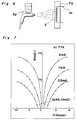
- The new phenomenon is explained below. Generally, the ceramic superconducting element shows a superconductive characteristics below a certain temperature, such as 77K, provided that no magnetic field is applied to the ceramic superconducting element. When magnetic field is applied to the ceramic superconducting element, but not greater than a threshold level H0, the ceramic superconducting element continues to show the superconductive characteristics, as shown in Fig. 1. Then, when the magnetic field applied to the superconducting element becomes equal to the threshold level H0, the superconducting element looses its superconductivity and suddenly shows magneto-resistance which increases at a high rate relative to the increase of the magnetic field. Thereafter, when the magnetic field is reduced to the threshold level H0, the magneto-resistance is also reduced to zero, again showing the superconductive characteristics. The same phenomenon is observed when the magnetic field is increased in the opposite polarity, as shown in Fig. 1.
- Since the resistance of the ceramic superconductive element is obtained by the application of magnetic field, the obtained resistance is referred to as a magneto-resistance, and such a phenomenon observed in the ceramic superconducting element is referred to as a superconducting magneto-resistance system.
- The superconducting magneto-resistance system can be understood as follows. When the ceramic superconductive element receives a magnetic field greater than the threshold level H0, the superconducting state of the crystal grain boundaries of the ceramic superconductor are destroyed by the applied magnetic field so that the superconductor changes from a superconducting state to an electrical resistance state.
- More specifically, when the ceramic superconducting element having crystal boundaries formed by the grains of a ceramic material is not receiving any magnetic field, the ceramic element shows no electrical resistance, as shown in Fig. 5. However, when a magnetic field greater than the threshold magnetic field H0 is applied, the ceramic element suddenly exhibits electrical resistance and the electrical resistance increases sharply as the applied magnetic field is increased. Since the rate of the change in resistance ΔR/ΔH at the threshold magnetic field H0 is as great as infinity, the logic device formed by the ceramic superconducting element utilizing superconducting magneto-resistance system will exhibit stable and high performance when compared with the conventional magneto-resistance elements.
- The trend in research in ceramic superconducting devices as being advanced by many research organizations today seeks to improve critical temperature (Tc), threshold magnetic field (H0), and threshold current (Jc) characteristics. In the research carried by the present inventors in the ceramic superconducting devices, the above mentioned phenomenon was found in specific types of superconductors (those having a weak coupling state between the grains of the superconducting body). The phenomenon is such that the superconducting state of these weak couplings is destroyed by a weak magnetic field (several gauss) as shown in Fig. 5, and thus exhibit electrical resistance, and that this resistance increases sharply with the increase in the strength of the applied magnetic field. This invention proposes a ceramic superconducting device which operates as a new type of logic circuit device using this phenomenon of a weak critical magnetic field.
- As shown in Fig. 2, the ceramic superconducting element comprises crystals of many superconducting fine grains in which an extremely thin insulator or resistor is interposed between the grains, but such grain boundaries exhibit zero electrical resistance, in which electrons move freely, due to the tunnel effect under the superconducting state. Or, the grains are contacted by a point. When juxtaposed grain boundaries exhibit a point contact in the so-called weak bond state, the superconductive state is obtained, and when a weak electrical field is applied, the point contacts are destroyed to exhibit ohmic resistance.
- In other words, a polycrystalline ceramic superconducting body in a weak bond state can equivalently form a bonded body of
multiple Josephson bonds 121, as shown in Fig. 2. - When a magnetic field is applied to a superconducting device of this type, the effects of the magnetic field break the superconducting state of
Josephson bonds 121, specifically, the superconducting weak bond state is broken by the application of a weak magnetic field so that the device exhibits electrical resistance, and the strength of this electrical resistance increases as the strength of the magnetic field is increased. - As will be clear from this principle as described above, this property is not dependent upon the direction of the applied magnetic field because the arrangement of the crystal grain boundaries is random, but is determined by the absolute value of the strength of the magnetic field.
- The present invention utilizes the weak bond existing at the crystal grain boundaries of a ceramic superconducting element. The device according to the present invention includes three conductive strips parallel or perpendicular to the superconducting device to provide different levels of magnetic field to the ceramic superconducting element by the electric current flowing through these conductive strips so as to change the ceramic superconducting element between superconductive and magneto-resistive states.
- In a preferred embodiment of the present invention, the ceramic superconducting element is made of Y₁Ba₂Cu₃O7-x, Bi₁Sr₁Ca₁Cu₂Ox, or any other ceramic superconducting film, and is formed in an elongated pattern. The electrical current conducting strips are made parallel or perpendicular to the ceramic superconducting film.
- In alternative embodiments of the aforementioned ceramic superconducting device, the three conductive strips which are provided on a single substrate, may be provided in a layered structure separated by an insulating material, or they may be juxtaposed with a parallel or perpendicular arrangement.
- Furthermore, in a preferred embodiment according to the present invention, each conductive strip is coupled with an independent current source.
- The features of the present invention will become apparent from the following description of preferred embodiments thereof with reference to the accompanying drawings, throughout which like parts are designated by like reference numerals, and in which:
- Fig. 1 is a graph showing the magneto-resistance change relative to the applied magnetic field strength in the ceramic superconducting element;
- Fig. 2 is a diagrammatic view of electric conductive passages formed in the ceramic superconductive material;
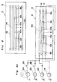
- Fig. 3 is a diagrammatic view of a logic device employing a ceramic superconducting element according to a preferred embodiment of the present invention;
- Figs. 4 and 5 are a graph showing condition change of the ceramic superconducting element by the application of magnetic field for performing IMPLICATION logic and EQUIVALENCE logic, respectively;
- Fig. 6 is a diagrammatic view showing a method for making the ceramic superconductive element on a substrate;
- Fig. 7 is a graph showing the magneto-resistance change relative to the applied magnetic field strength in the ceramic superconducting element for different electric currents applied to the ceramic superconducting element;
- Fig. 8 is a view similar to Fig. 3, but showing a modification thereof;
- Figs. 9a and 9b are views similar to Fig. 3, but showing further modifications thereof.
- Referring to Fig. 3, a logic device employing a ceramic superconducting element according to a preferred embodiment of the present invention is shown.
- In Fig. 3,
reference number 2 is a logic device including a ceramicsuperconducting element 4 deposited on asubstrate 3 and having an elongated configuration extending betweencurrent electrodes Current electrodes current supply electrodes superconducting element 4. - Connected intermediately along the ceramic
superconducting element 4 arevoltage electrodes superconducting element 4. - Extending closely adjacent and parallel to the ceramic
superconducting element 4 are threeelectrode strips superconducting element 4 by the control of electric current flowing through one, two or three of the three electrode strips. - In order to perform the IMPLICATION logic by the logic device of Fig. 3, DC
current sources electrodes current sources current source 22 is provided to supply DC current in the opposite direction, e.g., from right to left. Aswitch 26 is inserted betweencurrent source 22 andelectrode 14, and aswitch 28 is inserted betweencurrent source 24 andelectrode 16. - From
current sources electrodes superconducting element 4. - Determined by various factors, such as distance between the ceramic
superconducting element 4 andelectrode 12 and amount of current flowing throughelectrode 12, the magnetic field strength H1 is selected to satisfy the following inequality:
in which H0 is a threshold field strength of the ceramicsuperconducting element 4. As shown in Fig. 4, if the field strength in the ceramicsuperconducting element 4 is between -H0 and +H0, the ceramicsuperconducting element 4 maintains the superconductive state, and if the field strength in the ceramicsuperconducting element 4 increases greater than +H0 or decreases smaller than -H0, the ceramicsuperconducting element 4 exhibits magneto-resistive state. Thus, when switches 26 and 28 are turned off to provide only current I1, the ceramicsuperconducting element 4 receives magnetic field H1, makingelement 4 in the magneto-resistive state. - In a similar manner, the magnetic field strength H2 is selected to satisfy the following inequality:

Thus, whenswitch 26 is turned on and switch 28 is turned off to provide current -I2 in addition to current I1, the ceramicsuperconducting element 4 receives magnetic field H1-H2 which falls, as shown in Fig. 4, between -H0 and +H0, makingelement 4 in the superconductive state. - Furthermore, the magnetic field strength H3 is selected to satisfy the following inequality:

Thus, when switches 26 and 28 are both turned on to provide currents -I2 and I3 in addition to current I1, the ceramicsuperconducting element 4 receives magnetic field H1-H2+H3 which is greater than the threshold field strength H0, as shown in Fig. 4, makingelement 4 in the magneto-resistive state. - Also, when
switch 26 is turned off and switch 28 is turned on to provide current I3 in addition to current I1, the ceramicsuperconductive element 4 receives magnetic field H1+H3 which is greater than H0, as shown in Fig. 4, makingelement 4 in the magneto-resistive state. - If a current is applied to ceramic
superconductive element 4 from DC current source 18 a voltage drop will be observed acrosselement 4 betweenelectrodes superconductive element 4 is in the magneto-resistive state, but no voltage drop will be observed betweenelectrodes superconductive element 4 is in the superconductive state. - Accordingly, if the presence and absence of the current are indicated as "1" and "0", respectively, and the presence and absence of the voltage are also indicated as "1" and "0", respectively, the following Table C is obtained.

- As will be understood from Table C, input currents I2 and I3 and output voltage between
electrodes - It is to be noted that in order to meet the conditions of inequalities (1a), (1b) and (1c) indicated above,
current sources - In order to perform the EQUIVALENCE logic, DC
current source 24 is replaced by a DCcurrent source 25, shown by a dotted line in Fig. 3, which is provided to supply DC current from right to left when viewed in Fig. 3. - Thus, from
current sources electrodes superconducting element 4. - Similar to the above, the magnetic field strength H1 is selected to satisfy the following inequality:

Thus, when switches 26 and 28 are turned off to provide only current I1, the ceramicsuperconducting element 4 receives magnetic field H1, makingelement 4 in the magneto-resistive state, as understood from Fig. 5. - The magnetic field strength H2 is selected to satisfy the following inequality:

Thus, whenswitch 26 is turned on and switch 28 is turned off to provide current -I2 in addition to current I1, the ceramicsuperconducting element 4 receives magnetic field H1-H2 which falls, as shown in Fig. 5, between -H0 and +H0, makingelement 4 in the superconductive state. - Furthermore, the magnetic field strength H4 is selected to satisfy the following inequality:

Thus, when switches 26 and 28 are both turned on to provide currents -I2 and -I4 in addition to current I1, the ceramicsuperconducting element 4 receives magnetic field |H1-H2-H4| which is greater than the threshold field strength H0, as shown in Fig. 5, makingelement 4 in the magneto-resistive state. - Also, when
switch 26 is turned off and switch 28 is turned on to provide current -I4 in addition to current I1, the ceramicsuperconductive element 4 receives magnetic field H1-H4 which falls, as shown in Fig. 5, between -H0 and +H0, makingelement 4 in the superconductive state. - Accordingly, the following Table D is obtained, provided that the presence and absence of the current are indicated as "1" and "0", respectively, and the presence and absence of the voltage are also indicated as "1" and "0", respectively.

- As will be understood from Table D, input currents I2 and I4 and output voltage between
electrodes - It is to be noted that in order to meet the conditions of inequalities (2a), (2b) and (2c) indicated above,
current sources - In order to manufacture a ceramic
superconducting device 2 of the type used in the present invention, asubstrate 3 made of stabilized zirconia is heated by a heater Ht provided in a film forming apparatus Fa as shown in Fig. 6 to maintain a substrate temperature of 400°C. The ceramic material is a mixture of Y(NO₃)₃·6H₂O, Ba(NO₃)₂, and Cu(NO₃)₂.3H₂O weighed to form Y₁Ba₂Cu₃O₇-x, mixed in a nitrate solution which is sprayed intermittently by air sprayer Sp ontosubstrate 3 so as to form a film having a thickness of 5»m. Thus, a spray pyrolysis method may be used. The substrate and film are then baked at 950°C for 60 minutes and thereafter annealed in air for 10 hours at 500°C. Regarding the critical temperature of a ceramic superconducting film thus formed, resistance begins to drop from 100K, and loses all resistance at 83K. - Next, in order to process the high temperature ceramic superconducting film to a 50 »m wide, 30 mm long
superconducting body 4, thesubstrate 3 is applied with a photoresist and processed with conventional photolithography processes to form a fine striped shape, thus forming thesuperconducting element 4 onsubstrate 3. This ceramic high temperature superconducting element can be easily processed in a phosphoric acid etching agent. - Next, in order to manufacture the
electrodes - The ceramic
superconducting device 2 used in the present invention forms weak couplings due to the point contacts and insulating layer interposed between the grain boundaries, and may be thought of as an aggregation of Josephson junctions. Regarding the relationship between the applied magnetic field and electrical resistance shown in Fig. 7, magneto-resistance suddenly appears and increases rapidly when the strength of the magnetic field applied to the ceramic superconducting element, which has been in the superconductive state, exceeds a threshold level. Such a threshold level varies depending on the current flowing through the ceramic superconducting element. - When a 10 mA current is supplied to
electrode 12, formed of a Ti film, a magnetic field of 0.4 gauss can be obtained at a distance of 50 »m. Therefore, as apparent from the characteristics of the superconducting material shown in Fig. 7, when a 2 mA constant current is supplied to thesuperconducting element 4 throughterminals mΩ X 2 mA) output can be obtained. - According to one preferred embodiment, the ceramic
superconducting device 2 shown in Fig. 3 has such a arrangement that the centre to centre distance betweenelectrodes electrodes electrode 12 and ceramicsuperconducting element 4 is 50 »m, and the width of each ofelectrodes superconducting element 4 is 50 »m. - When the ceramic
superconducting device 2 of the above described construction is cooled to a temperature lower than 83K, and if no current is supplied toelectrodes superconductive element 4, an output voltage will not appear betweenelectrodes superconducting element 4 viaelectrodes case element 4 is maintained in the superconductive state. However, if a 10-mA current I1 is supplied to electrode 12 fromcurrent source 20, the magnetic field created by this current destroys the superconductive state ofelement 4, and produces magneto-resistance. Thus, a 20 »V output is obtained betweenelectrodes element 4. - It is to be noted that, according to the present invention as described above, the values of currents I1, I2, and I3 and the arrangement of
electrodes element 4 are not limited to those described above, but they may take any other amounts and sizes. For example, it is possible that currents I1, I2, and I3 supplied toelectrodes electrodes - In addition, the method for making
electrodes superconducting element 4 as described above should not be limited to the process as described above, but other processes, such as sputtering, MOCVD, or electron beam evaporation techniques may be used, as long as the same effects can be obtained. In particular,electrodes superconducting element 4 is made, thereby simplifying the manufacturing process. - Moreover, as apparent to those skilled in the art, while the ceramic high temperature superconducting film used in the present invention is Y₁Ba₂Cu₃O₇-x, the same effect may be obtained by using other high temperature superconductors as long as the grain boundaries form a weak coupling.
- Furthermore, the relationship of the positions of
superconducting element 4 andelectrodes electrode 12, may be formed on the opposite side ofsuperconducting body 4, as shown in Fig. 8. Moreover, the same effect may be obtained ifelectrodes - Also, as shown in Fig. 9a, only one
electrode 30 may be provided to receive currents from differentcurrent sources electrode 32 is provided for receiving currents in one direction and anotherelectrode 34 is provided for receiving currents in the other direction. - The present invention uses the properties of superconductivity, but does not use Josephson devices which use extremely thin insulation films which are extremely difficult to manufacture by conventional methods. Thus, the ceramic superconductive devices according to the present invention, which uses the weak coupling magneto-resistive effects of a superconducting element formed easily in the grain boundaries of a ceramic superconducting element, can be easily manufactured. Thus, the devices according to the present invention provide good noise resistance with a practical power supply for both input and output, and offer handling which is not difficult.
Claims (3)
- A logic device comprising:
a superconducting element (4) having magneto-resistive characteristics, provided on a substrate (3);
electrode means (12,14,16;30;32,34) arranged adjacent to said superconducting element; and
means for supplying current (20,22,24) to said electrode means so as to apply to said element a selected magnetic field to determine the conductive state of the element,
characterised in that:
said superconducting element (4) comprises ceramic superconductive material;
said electrode means is provided on said substrate (3) co-planar with said element; and
said means for supplying current comprises:
a first current source (20) which supplies a first current to said electrode means (12;30;32);
a second current source (22) which is switchably connected to supply a second current to said electrode means (14;30;34); and
a third current source (24) which is switchably connected to supply a third current to said electrode means (16;30;32);
said first and second currents, in combination, generating a net magnetic field which establishes a superconductive state of said element;
said first and third currents, in combination, generating a net magnetic field which establishes a magneto-resistive state of said element;
said first, second and third currents, in combination, generating a net magnetic field which establishes a magneto-resistive state of said element;
said logic device performing IMPLICATION operation. - A logic device comprising:
a superconducting element (4) having magneto-resistive characteristics, provided on a substrate (3);
electrode means (12,14,16;30;32,34) arranged adjacent to said superconducting element; and
means for supplying current (20,22,25) to said electrode means so as to apply to said element a selected magnetic field to determine the conductive state of the element,
characterised in that:
said superconducting element (4) comprises ceramic superconductive material;
said electrode means is provided on said substrate (3) co-planar with said element; and
said means for supplying current comprises:
a first current source (20) which supplies a first current to said electrode means (12;30;32);
a second current source (22) which is switchably connected to supply a second current to said electrode means (14;30;34); and
a third current source (25) which is switchably connected to supply a third current to said electrode means (16;30;32);
said first and second currents, in combination, generating a net magnetic field which establishes a superconductive state of said element;
said first and third currents, in combination, generating a net magnetic field which establishes a superconductive state of said element;
said first, second and third currents, in combination, generating a net magnetic field which establishes a magneto-resistive state of said element;
said logic device performing EQUIVALENCE operation. - A logic device according to claim 1 or claim 2, wherein said electrode means comprises:
a first electrode (12) connected to said first current source (20);
a second electrode (14) switchably connected to said second current source (22); and
a third electrode (16) switchably connected to said third current source (24;25);
said first, second and third electrodes each being provided on said substrate (3) adjacent to and co-planar with said superconducting element (4).
Applications Claiming Priority (4)
| Application Number | Priority Date | Filing Date | Title |
|---|---|---|---|
| JP148576/88 | 1988-06-16 | ||
| JP63148576A JPH081969B2 (en) | 1988-06-16 | 1988-06-16 | Ceramic superconducting device |
| JP148577/88 | 1988-06-16 | ||
| JP63148577A JPH01316978A (en) | 1988-06-16 | 1988-06-16 | Ceramic superconductive memory element |
Publications (3)
| Publication Number | Publication Date |
|---|---|
| EP0347258A2 EP0347258A2 (en) | 1989-12-20 |
| EP0347258A3 EP0347258A3 (en) | 1990-11-07 |
| EP0347258B1 true EP0347258B1 (en) | 1995-05-24 |
Family
ID=26478728
Family Applications (1)
| Application Number | Title | Priority Date | Filing Date |
|---|---|---|---|
| EP89306161A Expired - Lifetime EP0347258B1 (en) | 1988-06-16 | 1989-06-16 | Logic device using ceramic superconducting element |
Country Status (4)
| Country | Link |
|---|---|
| US (1) | US5041880A (en) |
| EP (1) | EP0347258B1 (en) |
| CN (1) | CN1020363C (en) |
| DE (1) | DE68922786T2 (en) |
Families Citing this family (25)
| Publication number | Priority date | Publication date | Assignee | Title |
|---|---|---|---|---|
| US5332722A (en) * | 1987-12-02 | 1994-07-26 | Sumitomo Electric Industries, Ltd | Nonvolatile memory element composed of combined superconductor ring and MOSFET |
| JPH04302178A (en) * | 1990-12-21 | 1992-10-26 | Texas Instr Inc <Ti> | Apparatus and method for storing information in magnetic field |
| WO1992020092A1 (en) * | 1991-05-08 | 1992-11-12 | Superconductor Technologies, Inc. | Passivation coating for superconducting thin film device |
| US5930165A (en) * | 1997-10-31 | 1999-07-27 | The United States Of America As Represented By The Secretary Of The Navy | Fringe field superconducting system |
| US7615385B2 (en) | 2006-09-20 | 2009-11-10 | Hypres, Inc | Double-masking technique for increasing fabrication yield in superconducting electronics |
| WO2019160573A2 (en) | 2017-05-16 | 2019-08-22 | PsiQuantum Corp. | Superconducting signal amplifier |
| WO2019160572A2 (en) | 2017-05-16 | 2019-08-22 | PsiQuantum Corp. | Gated superconducting photon detector |
| US10566516B2 (en) | 2017-07-28 | 2020-02-18 | PsiQuantum Corp. | Photodetector with superconductor nanowire transistor based on interlayer heat transfer |
| US10361703B2 (en) | 2017-10-05 | 2019-07-23 | PsiQuantum Corp. | Superconducting logic circuits |
| US10461445B2 (en) | 2017-11-13 | 2019-10-29 | PsiQuantum Corp. | Methods and devices for impedance multiplication |
| WO2019157077A1 (en) | 2018-02-06 | 2019-08-15 | PsiQuantum Corp. | Superconducting photon detector |
| WO2019160869A1 (en) | 2018-02-14 | 2019-08-22 | PsiQuantum Corp. | Superconducting logic components |
| WO2019213147A1 (en) | 2018-05-01 | 2019-11-07 | PsiQuantum Corp. | Photon number resolving superconducting detector |
| US10984857B2 (en) | 2018-08-16 | 2021-04-20 | PsiQuantum Corp. | Superconductive memory cells and devices |
| US10573800B1 (en) | 2018-08-21 | 2020-02-25 | PsiQuantum Corp. | Superconductor-to-insulator devices |
| US11101215B2 (en) | 2018-09-19 | 2021-08-24 | PsiQuantum Corp. | Tapered connectors for superconductor circuits |
| US11719653B1 (en) | 2018-09-21 | 2023-08-08 | PsiQuantum Corp. | Methods and systems for manufacturing superconductor devices |
| US10944403B2 (en) | 2018-10-27 | 2021-03-09 | PsiQuantum Corp. | Superconducting field-programmable gate array |
| US11289590B1 (en) | 2019-01-30 | 2022-03-29 | PsiQuantum Corp. | Thermal diode switch |
| US11569816B1 (en) | 2019-04-10 | 2023-01-31 | PsiQuantum Corp. | Superconducting switch |
| US11009387B2 (en) | 2019-04-16 | 2021-05-18 | PsiQuantum Corp. | Superconducting nanowire single photon detector and method of fabrication thereof |
| US11380731B1 (en) | 2019-09-26 | 2022-07-05 | PsiQuantum Corp. | Superconducting device with asymmetric impedance |
| US11585695B1 (en) | 2019-10-21 | 2023-02-21 | PsiQuantum Corp. | Self-triaging photon detector |
| US11994426B1 (en) | 2019-11-13 | 2024-05-28 | PsiQuantum Corp. | Scalable photon number resolving photon detector |
| KR102706220B1 (en) * | 2020-01-17 | 2024-09-13 | 양쯔 메모리 테크놀로지스 씨오., 엘티디. | Advanced memory structures and devices |
Family Cites Families (11)
| Publication number | Priority date | Publication date | Assignee | Title |
|---|---|---|---|---|
| US3093754A (en) * | 1960-06-03 | 1963-06-11 | Space Technology Lab Inc | Superconductor and gate employing single elongated, simply connected thin film as gate element |
| US3196408A (en) * | 1961-05-24 | 1965-07-20 | Ibm | Superconductive storage circuits |
| FR1381497A (en) * | 1962-11-01 | 1964-12-14 | Thomson Houston Comp Francaise | Superconducting switching device |
| US3281609A (en) * | 1964-01-17 | 1966-10-25 | Bell Telephone Labor Inc | Cryogenic supercurrent tunneling devices |
| US3758795A (en) * | 1972-06-30 | 1973-09-11 | Ibm | Superconductive circuitry using josephson tunneling devices |
| CH643967A5 (en) * | 1979-05-29 | 1984-06-29 | Ibm | SUPERCONDUCTIVE SWITCHING AND STORAGE DEVICE. |
| JPS6010451B2 (en) * | 1979-08-27 | 1985-03-18 | 工業技術院長 | Switching circuit using Josephson effect |
| JPS6065582A (en) * | 1983-09-20 | 1985-04-15 | Nippon Telegr & Teleph Corp <Ntt> | Grain boundary josephson junction photodetector |
| JPS6464377A (en) * | 1987-09-04 | 1989-03-10 | Matsushita Electric Industrial Co Ltd | Superconducting coupler |
| JPS6489479A (en) * | 1987-09-30 | 1989-04-03 | Hitachi Ltd | Superconducting circuit device |
| US5070070A (en) * | 1988-03-09 | 1991-12-03 | E. I. Du Pont De Nemours And Company | High temperature superconducting memory storage device and cryotron |
-
1989
- 1989-06-14 US US07/365,921 patent/US5041880A/en not_active Expired - Lifetime
- 1989-06-16 EP EP89306161A patent/EP0347258B1/en not_active Expired - Lifetime
- 1989-06-16 CN CN89104039A patent/CN1020363C/en not_active Expired - Fee Related
- 1989-06-16 DE DE68922786T patent/DE68922786T2/en not_active Expired - Fee Related
Non-Patent Citations (4)
| Title |
|---|
| JPN. J. APPL. PHYS., vol. 21, Supplement 21-1 (1982), pp. 313-318 * |
| NATURE, vol.328, 2 July 1987, pp. 47-48. * |
| PROCEEDINGS OF THE IEEE, vol. 70, no. 1, January 1982, pp. 26-34. * |
| SCIENTIFIC AMERICAN, vol. 242, no. 5, May 1980, pp. 38-53. * |
Also Published As
| Publication number | Publication date |
|---|---|
| US5041880A (en) | 1991-08-20 |
| CN1020363C (en) | 1993-04-21 |
| CN1039154A (en) | 1990-01-24 |
| DE68922786T2 (en) | 1995-11-23 |
| EP0347258A2 (en) | 1989-12-20 |
| DE68922786D1 (en) | 1995-06-29 |
| EP0347258A3 (en) | 1990-11-07 |
Similar Documents
| Publication | Publication Date | Title |
|---|---|---|
| US5041880A (en) | Logic device and memory device using ceramic superconducting element | |
| Maezawa et al. | Overdamped Josephson junctions with Nb/AlO x/Al/AlO x/Nb structure for integrated circuit application | |
| JPH01170080A (en) | Superconducting fet element | |
| US5849669A (en) | High temperature superconducting Josephson device and method for manufacturing the same | |
| JPH0834320B2 (en) | Superconducting element | |
| US5430013A (en) | Superconducting thin film formed of oxide superconductor material, superconducting current path and superconducting device utilizing the superconducting thin film | |
| RU2343591C1 (en) | Josephson- transition super-conducting device | |
| JP2583922B2 (en) | Superconducting switching element | |
| US4888622A (en) | Superconductor electron device | |
| US5656575A (en) | Method and apparatus for fabricating weak link junctions on vicinally cut substrates | |
| EP0618626A1 (en) | Josephson junction device of oxide superconductor having low noise level at liquid nitrogen temperature | |
| JP2583923B2 (en) | Superconducting switching element | |
| JP2867956B2 (en) | Superconducting transistor | |
| Sakai et al. | Investigation of IV characteristics of intrinsic Josephson junctions in Bi-2223 thin films | |
| JPH02194667A (en) | Superconducting transistor and manufacture thereof | |
| JP2583924B2 (en) | Superconducting switching element | |
| JP3287743B2 (en) | Superconducting logic gate | |
| JP2679610B2 (en) | Superconducting element manufacturing method | |
| JP2955407B2 (en) | Superconducting element | |
| EP0571633A1 (en) | Superconductive element | |
| JP2649808B2 (en) | Current injection cryotron | |
| JPH02273975A (en) | Superconducting switching element | |
| JPH0831625B2 (en) | Superconducting 3-terminal element | |
| JPS6256672B2 (en) | ||
| JPH0955546A (en) | High-speed logic gate using intrinsic junction |
Legal Events
| Date | Code | Title | Description |
|---|---|---|---|
| PUAI | Public reference made under article 153(3) epc to a published international application that has entered the european phase |
Free format text: ORIGINAL CODE: 0009012 |
|
| AK | Designated contracting states |
Kind code of ref document: A2 Designated state(s): CH DE FR GB IT LI NL |
|
| PUAL | Search report despatched |
Free format text: ORIGINAL CODE: 0009013 |
|
| AK | Designated contracting states |
Kind code of ref document: A3 Designated state(s): CH DE FR GB IT LI NL |
|
| 17P | Request for examination filed |
Effective date: 19901214 |
|
| 17Q | First examination report despatched |
Effective date: 19930622 |
|
| GRAA | (expected) grant |
Free format text: ORIGINAL CODE: 0009210 |
|
| AK | Designated contracting states |
Kind code of ref document: B1 Designated state(s): CH DE FR GB IT LI NL |
|
| PG25 | Lapsed in a contracting state [announced via postgrant information from national office to epo] |
Ref country code: IT Free format text: LAPSE BECAUSE OF FAILURE TO SUBMIT A TRANSLATION OF THE DESCRIPTION OR TO PAY THE FEE WITHIN THE PRE;WARNING: LAPSES OF ITALIAN PATENTS WITH EFFECTIVE DATE BEFORE 2007 MAY HAVE OCCURRED AT ANY TIME BEFORE 2007. THE CORRECT EFFECTIVE DATE MAY BE DIFFERENT FROM THE ONE RECORDED.SCRIBED TIME-LIMIT Effective date: 19950524 Ref country code: LI Effective date: 19950524 Ref country code: CH Effective date: 19950524 Ref country code: NL Free format text: LAPSE BECAUSE OF NON-PAYMENT OF DUE FEES Effective date: 19950524 |
|
| REF | Corresponds to: |
Ref document number: 68922786 Country of ref document: DE Date of ref document: 19950629 |
|
| ET | Fr: translation filed | ||
| REG | Reference to a national code |
Ref country code: CH Ref legal event code: PL |
|
| NLV1 | Nl: lapsed or annulled due to failure to fulfill the requirements of art. 29p and 29m of the patents act | ||
| PLBE | No opposition filed within time limit |
Free format text: ORIGINAL CODE: 0009261 |
|
| STAA | Information on the status of an ep patent application or granted ep patent |
Free format text: STATUS: NO OPPOSITION FILED WITHIN TIME LIMIT |
|
| 26N | No opposition filed | ||
| REG | Reference to a national code |
Ref country code: GB Ref legal event code: IF02 |
|
| PGFP | Annual fee paid to national office [announced via postgrant information from national office to epo] |
Ref country code: GB Payment date: 20020612 Year of fee payment: 14 |
|
| PGFP | Annual fee paid to national office [announced via postgrant information from national office to epo] |
Ref country code: FR Payment date: 20020626 Year of fee payment: 14 |
|
| PGFP | Annual fee paid to national office [announced via postgrant information from national office to epo] |
Ref country code: DE Payment date: 20020725 Year of fee payment: 14 |
|
| PG25 | Lapsed in a contracting state [announced via postgrant information from national office to epo] |
Ref country code: GB Free format text: LAPSE BECAUSE OF NON-PAYMENT OF DUE FEES Effective date: 20030616 |
|
| PG25 | Lapsed in a contracting state [announced via postgrant information from national office to epo] |
Ref country code: DE Free format text: LAPSE BECAUSE OF NON-PAYMENT OF DUE FEES Effective date: 20040101 |
|
| GBPC | Gb: european patent ceased through non-payment of renewal fee |
Effective date: 20030616 |
|
| PG25 | Lapsed in a contracting state [announced via postgrant information from national office to epo] |
Ref country code: FR Free format text: LAPSE BECAUSE OF NON-PAYMENT OF DUE FEES Effective date: 20040227 |
|
| REG | Reference to a national code |
Ref country code: FR Ref legal event code: ST |