EP0346572A2 - Circuit arrangement for the transmission of binary signals - Google Patents
Circuit arrangement for the transmission of binary signals Download PDFInfo
- Publication number
- EP0346572A2 EP0346572A2 EP89104406A EP89104406A EP0346572A2 EP 0346572 A2 EP0346572 A2 EP 0346572A2 EP 89104406 A EP89104406 A EP 89104406A EP 89104406 A EP89104406 A EP 89104406A EP 0346572 A2 EP0346572 A2 EP 0346572A2
- Authority
- EP
- European Patent Office
- Prior art keywords
- voltage
- signal
- bus line
- diode
- capacitor
- Prior art date
- Legal status (The legal status is an assumption and is not a legal conclusion. Google has not performed a legal analysis and makes no representation as to the accuracy of the status listed.)
- Withdrawn
Links
Images

Classifications
-
- H—ELECTRICITY
- H04—ELECTRIC COMMUNICATION TECHNIQUE
- H04L—TRANSMISSION OF DIGITAL INFORMATION, e.g. TELEGRAPHIC COMMUNICATION
- H04L25/00—Baseband systems
- H04L25/02—Details ; arrangements for supplying electrical power along data transmission lines
- H04L25/0264—Arrangements for coupling to transmission lines
- H04L25/0292—Arrangements specific to the receiver end
-
- H—ELECTRICITY
- H04—ELECTRIC COMMUNICATION TECHNIQUE
- H04L—TRANSMISSION OF DIGITAL INFORMATION, e.g. TELEGRAPHIC COMMUNICATION
- H04L12/00—Data switching networks
- H04L12/28—Data switching networks characterised by path configuration, e.g. LAN [Local Area Networks] or WAN [Wide Area Networks]
- H04L12/40—Bus networks
-
- H—ELECTRICITY
- H04—ELECTRIC COMMUNICATION TECHNIQUE
- H04L—TRANSMISSION OF DIGITAL INFORMATION, e.g. TELEGRAPHIC COMMUNICATION
- H04L25/00—Baseband systems
- H04L25/02—Details ; arrangements for supplying electrical power along data transmission lines
- H04L25/0264—Arrangements for coupling to transmission lines
- H04L25/0266—Arrangements for providing Galvanic isolation, e.g. by means of magnetic or capacitive coupling
-
- H—ELECTRICITY
- H04—ELECTRIC COMMUNICATION TECHNIQUE
- H04L—TRANSMISSION OF DIGITAL INFORMATION, e.g. TELEGRAPHIC COMMUNICATION
- H04L25/00—Baseband systems
- H04L25/02—Details ; arrangements for supplying electrical power along data transmission lines
- H04L25/0264—Arrangements for coupling to transmission lines
- H04L25/0272—Arrangements for coupling to multiple lines, e.g. for differential transmission
-
- H—ELECTRICITY
- H04—ELECTRIC COMMUNICATION TECHNIQUE
- H04L—TRANSMISSION OF DIGITAL INFORMATION, e.g. TELEGRAPHIC COMMUNICATION
- H04L25/00—Baseband systems
- H04L25/02—Details ; arrangements for supplying electrical power along data transmission lines
- H04L25/0264—Arrangements for coupling to transmission lines
- H04L25/028—Arrangements specific to the transmitter end
Definitions
- the invention relates to a circuit arrangement for transmitting binary signals according to the preamble of claim 1.
- DE-OS 30 15 661 describes a circuit arrangement for transmitting binary signals via a bus line, which is connected to a first voltage source via resistors that are equal to the characteristic impedance.
- the stations connected to the bus line switch the bus line to a second voltage source.
- the receivers essentially consist of a comparator that is galvanically connected to the bus line and that compares the voltage on the bus line with a reference voltage.
- a bus line with an ohmic resistance of 80 ohms and a characteristic impedance of 120 ohms is fed at one end with a voltage of 12 volts via a resistor of 120 ohms and is terminated at the other end with the characteristic impedance, then changes to one in
- the receiver located close to the supply voltage source changes the voltage from 7.5 volts to 4.8 volts when a transmitter at the other end of the line transmits.
- the voltage at this end drops from 4.5 volts to 0 volts when a transmitter closer to the supply voltage source is operating. This effect is particularly disruptive if the receivers are galvanically isolated from the bus line by means of a transmitter, since they do not easily transmit binary signals. If a data signal is not free of direct current, the transmitter can go into saturation, as a result of which part of the information is no longer transmitted.
- DE-AS 20 50 994 therefore describes a method in which a transformer is fed with a periodic signal via a first winding.
- An electronic switch which is controlled by the binary signals, is connected in parallel to a second winding.
- this switch In one of the two states of the binary signal, e.g. B. at the signal log. "0", this switch is open so that it does not dampen the second winding and the periodic signal is transmitted to a third winding to which a rectifier is connected.
- the binary signal is log. "1”
- the switch shorts the second winding so that the periodic signal is no longer transmitted to the third winding and the voltage at the output of the rectifier becomes zero.
- the binary signal is thus transmitted, and a signal state can exist for any length of time.
- the present invention has for its object to provide an arrangement for transmitting binary signals according to the preamble of claim 1, which allows an inductive coupling of the receiver to the bus line even if the signal levels on the bus line are different for the same binary signal states.
- this object is achieved with the measures specified in the characterizing part of claim 1. It is advisable to clamp on the voltage that is on the bus line when the switches of all transmitters are open. This voltage varies from receiver to receiver, but remains constant for the individual receivers, so that the capacitors are not recharged.
- the receivers equipped according to the invention do not need to be set according to the point at which they are coupled to the bus line. With the new arrangement, any binary signals, including those with a DC component, can be transmitted.
- the clamping circuit advantageously contains a diode which forms a series circuit between the wires of the bus line with the capacitor.
- the comparator can consist of a transistor, the control path of which is parallel to the diode, in such a way that when the diode is operated in the forward direction, the transistor is blocked, and that when a blocking voltage is connected to the diode, the transistor is conductive State is controlled.
- BL1, BL2 denote two wires of a bus line, at one end of which a voltage source SQ is connected via a resistor RZ1, which is equal to the characteristic impedance of the bus line. At the other end, the bus line is terminated with a resistor RZ2, also with the characteristic impedance.
- a minimum current of z. B. 50 mA which can be used for monitoring for line break.
- the resistor RZ1 is not only used for reflection free transmission, but also to limit the current in the event of a short circuit.
- Several stations ST1 ... STn are connected in parallel to the bus line, each of which contains a transmitter S1, Sn and a receiver E1, En, among others.
- the station ST1 can be accommodated as a central station in the control room.
- a transformer U1 has three windings W1, W2, W3.
- the winding W2 is the collector-emitter path of a transistor T2 connected in parallel, the base electrode of which is supplied with the binary signal to be transmitted.
- the winding W3 is fed with a high-frequency, periodic clock signal, which can be a sinusoidal signal, and whose frequency is significantly higher than that of the clock frequency of the binary signal.
- the transistor T2 is blocked, the winding W2 is then virtually undamped, and the clock signal is transmitted to the winding W1 and rectified there by a diode D1.
- the positive voltage occurring at a smoothing capacitor C1 controls a transistor T1, so that its collector-emitter path short-circuits the two wires BL1, BL2 of the bus line. This reduces the voltage on the bus line at all stations. If the transistor T2 is supplied with a binary signal of level H, it short-circuits the winding W2 and the transformer U1 is damped in such a way that the clock signal is not transmitted to the winding W1. The transistor T1 is therefore blocked and does not load the bus line.
- the binary signals emitted by a transmitter are received by the receivers of all stations, including that of the station which contains the transmitter emitting the binary signal. This allows the stations to check their own transmitters.
- the voltage source SQ outputs a voltage of 12 volts
- the values of the resistors RZ1, RZ2 and the characteristic impedance of the bus line are each 120 ohms and the wires BL1, BL2 each have an ohmic resistance of 40 ohms to have.
- the station ST1 is connected to the bus line in the immediate vicinity of the voltage source SQ and the resistor RZ1, and the station STn in the immediate vicinity of the terminating resistor RZ2. Under these assumptions, there is a voltage of 7.5 volts on station ST1 and a voltage of 4.5 volts on station STn on the bus line if all transmitters emit binary signal H.
- the transmitter -S1 sends the signal L
- the voltage on the bus line drops to 0 volts if the residual voltage of the transistor T1 is not taken into account for the sake of simplicity.
- the transmitter Sn emits the signal L
- the voltage at the receiver E1 only drops to about 4.8 volts, at the station STn, however, to the residual voltage of the switching transistor.
- the voltages at the intermediate stations are between those at the stations ST1 and STn. Therefore, completely different voltages occur at the individual stations.
- the problem of the different voltage levels is solved in the receivers, which are constructed in accordance, by means of a clamping circuit.
- the function of the receiver is explained in more detail using the circuit diagram of the receiver En.
- the receivers each contain a transformer U2 with three windings W4, W5, W6.
- a high-frequency clock signal is supplied to the latter, which is expediently taken from the same source as the signal with which the winding W3 of the transmitter-transformer U1 is fed. If the signal H is on the bus line, a capacitor C2 is charged with the voltage occurring at this level via a diode D2. The capacitor voltage is equal to the voltage on the bus line reduced by the forward voltage of the diode D2. A transistor T3 is blocked.
- the clock signal supplied to the winding W6 is therefore transmitted to the winding W5, to which a rectifier with a diode D3 and a filter capacitor C3 is connected, at the output of which a level corresponding to the signal H occurs.
- the signal L is set on the bus line, the diode D2 blocks and the transistor T3 is turned on, so that the clock pulses are no longer transmitted from the winding W6 to the winding W5.
- the output voltage of diode D3 becomes zero According to the signal L, ie the signals H and L are transmitted from the input of the respectively controlled transmitter transistor T2 to the outputs of all receiver diodes D3.
- the minimum voltage difference between the levels of the H and L signals is equal to the sum of the forward voltage of the diode D2 and the switch-on control voltage of the transistor T3.
- the required minimum voltage swing on the bus line can be increased by connecting a plurality of diodes D2 in series or switching on one or more diodes in the emitter circuit of transistor T3.
- the response threshold will expediently be set to about half the smallest voltage swing occurring on the bus line. In the exemplary embodiment, the smallest voltage swing of 2.8 volts occurs at station ST1. The response threshold is therefore set to 1 to 1.5 volts, which is approximately achieved with the receiver circuit shown.
- the transistor T3 represents a comparator which compares the capacitor voltage C2 with the respective voltage on the bus line and emits a signal or damps the winding W4 when the signal swing exceeds the predetermined value. No supply voltage is supplied to the parts of the stations arranged between the bus line and the transmitters in accordance with the required galvanic isolation.
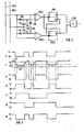
- FIG. 2 shows the circuit diagram of a receiver with two switching thresholds, the use of which may be necessary if the signals on the bus line, the wires of which are designated BL3, BL4, are severely distorted.
- the receiving circuit contains two clamping circuits, each consisting of a series circuit with a capacitor C3 or C4 and a diode D4 or D5 and between the wires BL3, BL4 of the bus line.
- a comparator VGL1, VGL2 is connected to each diode.
- the series circuit D4, C3 corresponds to the clamping circuit D2, C2 of the circuit according to FIG. 1, the comparator to the transistor T3.
- the anode of the diode D4 and the cathode of the diode D5 are connected to the positive voltage-carrying wire BL3.
- a high-resistance resistor R1 is connected in parallel with the capacitor C3.
- the potential at the non-inverting input of the comparator VGL2 is drawn via a high-resistance resistor R2, to which a diode D6 is connected in series in the exemplary embodiment, with a time constant that is large in comparison with the pulse duration, against the potential on the bus line BL3, so that signals with a different voltage swing can be detected.
- the clock inputs of bistable flip-flops FF1, FF2 are connected to the outputs of the comparators VGL1, VGL2, in such a way that the flip-flops take over the signal supplied to their preparation inputs D on negative edges.
- the preparation input D of the flip-flop FF1 is connected to the output Q of the flip-flop F F 2, the preparation input D of the flip-flop FF2 to the output Q of the flip-flop FF1.
- the outputs Q of both flip-flops are led to an exclusive OR gate EXO, at whose output the regenerated input signal appears.
- FIG. 3 shows the time diagram a the output signal of a transmitter, the diagram b the input signal of the receiver under consideration, the signals v1, v2 the output signals of its comparators VGL1 and VGL2, the diagrams f1, f2 the outputs Q of the flip-flops FF1, FF2 occurring signals and the diagram xr the output signal of the EXCLUSIVE OR element EXO.
- the positive voltage U 1 lies between the wires BL3, BL4 of the bus line.
- a small current flows through the clamping diode D4 and the resistor R1, so that a voltage of approximately 0.7 V drops at the clamping diode.
- the capacitor C3 is therefore charged to the voltage U 1 reduced by the forward voltage of the diode D4.
- the forward voltage of the diode D4 is at the input of the comparator VGL1, its output signal is therefore H, corresponding to log. "1".
- the condenser Gate C4 charged via diode D6 and resistor R2 to approximately the same value as capacitor C3, so that at the input of comparator VGL2 there is approximately the same voltage as at the input of comparator VGL1, but with different polarity. Its output signal v2 is therefore log. "0". If the transmitter, which is spatially distant from the described receiver, sends a zero signal to the bus line, the input voltage slowly drops due to the capacity of the bus line and the modules connected to it compared to the output signal of the transmitter.
- the transmitter gives a "1" signal on the bus line and the input signal rises there, a negative edge occurs in the output signal v2, which switches the flip-flop FF2.
- the output signal xr is therefore log like the output signal a of the transmitter. "1”. If the input signal e reaches the threshold voltage 51, the comparator VGL1 also switches over. However, the positive edge of its output signal v11 has no effect, so that the signal xr does not change.
- the flip-flop FF1 is only switched over with the negative flank of the signal v1 on the following negative flank of the input signal, when the threshold S1 falls below again, and the signal xr follows the signal a switched by the transmitter to the bus line.
- the threshold S2 is entered as constant for the sake of clarity. In fact, this threshold rises during times when the voltage of the input signal is greater than U2 due to the charging of the capacitor C4 the diode D6 and the resistor R2 slowly on. On the other hand, the capacitor C4 is recharged via the diode D5 during the phases of low input voltage. This means that the circuit always adapts to the lower value U2 of the input voltage. The input signals are therefore reliably detected and restored, irrespective of the position of the bus line on which the respective transmitter is located.
- the exemplary embodiment can be modified in many ways. So z. B. the diode D6 can be dispensed with and the high-resistance resistor R2 can be connected directly to the cathode of the diode D4. Furthermore, the comparators can be reversed, flip-flops can be used which switch not on the negative edges but on the positive, and the preparatory inputs of the flip-flops can be connected in a different way to the outputs of the other stage. These measures must of course be taken in a suitable combination. It is essential that there are two clamping circuits for the two input signal levels and that the current input signal level is compared with the clamping potentials and the comparison results are logically combined so that the input signal is restored.
Landscapes
- Engineering & Computer Science (AREA)
- Computer Networks & Wireless Communication (AREA)
- Signal Processing (AREA)
- Power Engineering (AREA)
- Dc Digital Transmission (AREA)
- Small-Scale Networks (AREA)
Abstract
Die an eine Busleitung (BL1, BL2) angeschlossenen Empfänger (E1, En) enthalten je eine Klemmschaltung, mit der die Eingangsspannung auf den Signalpegel geklemmt wird, der bei einem der beiden Zustände von binären Signalen auf der Busleitung (BL1, BL2) auftritt. Ein Vergleicher (T3) gibt ein den zweiten Zustand der binären Signale anzeigendes Signal ab, wenn die Differenz zwischen dem Klemmpotential und dem auf der Busleitung auftretenden Signalpegel einen vorgegebenen Wert übersteigt. Mit dem Ausgangssignai des Vergleichers (T3) wird ein mit hochfrequenten Taktimpulsen gespeister Übertrager (U2) gesteuert.The receivers (E1, En) connected to a bus line (BL1, BL2) each contain a clamping circuit with which the input voltage is clamped to the signal level that occurs in one of the two states of binary signals on the bus line (BL1, BL2). A comparator (T3) outputs a signal indicating the second state of the binary signals when the difference between the terminal potential and the signal level occurring on the bus line exceeds a predetermined value. The output signal of the comparator (T3) is used to control a transformer (U2) fed with high-frequency clock pulses.
Die Erfindung wird in Bussystemen angewendet, deren Empfänger von der Busleitung mittels eines Übertragers galvanisch getrennt sind. 
Description
Die Erfindung betrifft eine Schaltungsanordnung zum Übertragen von binären Signalen gemäß dem Oberbegriff des Anspruchs 1.The invention relates to a circuit arrangement for transmitting binary signals according to the preamble of
In der DE-OS 30 15 661 ist eine Schaltungsanordnung zum Übertragen von binären Signalen über eine Busleitung beschrieben, die über Widerstände, die gleich dem Wellenwiderstand sind, an eine erste Spannungsquelle angeschlossen ist. Zum Senden von binären Signalen schalten die an die Busleitung angeschlossenen Stationen die Busleitung an eine zweite Spannungsquelle. Die Empfänger bestehen im wesentlichen aus einem Vergleicher, der galvanisch an die Busleitung angeschlossen ist und der die Spannung auf der Busleitung mit einer Referenzspannung vergleicht. Vor allem bei prozeßtechnischen Anwendungen ist es häufig nicht möglich, an beide Enden der Busleitung eine Speisespannungsquelle anzuschließen, und die Empfänger und Sender müssen galvanisch von der Busleitung getrennt sein. Es tritt dann das Problem auf, daß an den Empfängern Signalpegel auftreten, die je nach Anschlußort von Sender und Empfänger unterschiedlich sind. Wenn z. B. eine Busleitung mit einem ohmschen Widerstand von 80 Ohm und einem Wellenwiderstand von 120 Ohm an einem Ende mit einer Spannung von 12 Volt über einen Widerstand von 120 Ohm gespeist wird und am anderen Ende mit dem Wellenwiderstand abgeschlossen ist, so ändert sich an einem in der Nähe der Speisespannungsquelle liegenden Empfänger die Spannung von 7,5 Volt auf 4,8 Volt, wenn ein am andern Ende der Leitung liegender Sender sendet. Dagegen sinkt die Spannung an diesem Ende von 4,5 Volt auf 0 Volt, wenn ein näher an der Speisespannungsquelle liegender Sender arbeitet. Dieser Effekt ist vor allem dann störend, wenn die Empfänger von der Busleitung mittels eines Übertragers galvanisch getrennt sind, da diese nicht ohne weiteres binäre Signale einwandfrei übertragen. Ist nämlich ein Datensignal nicht gleichstromfrei, kann der Übertrager in Sättigung gehen, wodurch ein Teil der Information nicht mehr übertragen wird.DE-OS 30 15 661 describes a circuit arrangement for transmitting binary signals via a bus line, which is connected to a first voltage source via resistors that are equal to the characteristic impedance. To send binary signals, the stations connected to the bus line switch the bus line to a second voltage source. The receivers essentially consist of a comparator that is galvanically connected to the bus line and that compares the voltage on the bus line with a reference voltage. Especially in process engineering applications, it is often not possible to connect a supply voltage source to both ends of the bus line, and the receivers and transmitters must be electrically isolated from the bus line. The problem then arises that signal levels occur at the receivers, which differ depending on the connection location of the transmitter and receiver. If e.g. B. a bus line with an ohmic resistance of 80 ohms and a characteristic impedance of 120 ohms is fed at one end with a voltage of 12 volts via a resistor of 120 ohms and is terminated at the other end with the characteristic impedance, then changes to one in The receiver located close to the supply voltage source changes the voltage from 7.5 volts to 4.8 volts when a transmitter at the other end of the line transmits. On the other hand, the voltage at this end drops from 4.5 volts to 0 volts when a transmitter closer to the supply voltage source is operating. This effect is particularly disruptive if the receivers are galvanically isolated from the bus line by means of a transmitter, since they do not easily transmit binary signals. If a data signal is not free of direct current, the transmitter can go into saturation, as a result of which part of the information is no longer transmitted.
Die DE-AS 20 50 994 beschreibt daher ein Verfahren, bei dem ein Übertrager über eine erste Wicklung mit einem periodischen Signal gespeist wird. Zu einer zweiten Wicklung ist ein elektronischer Schalter parallelgeschaltet, der von den binären Signalen gesteuet wird. Bei einem der beiden Zustände des binären Signals, z. B. beim Signal log. "0", ist dieser Schalter geöffnet, so daß er nicht die zweite Wicklung bedämpft und das periodische Signal zu einer dritten Wicklung übertragen wird, an die ein Gleichrichter angeschlossen ist. Ist das binäre Signal dagegen log. "1", schließt der Schalter die zweite Wicklung kurz, so daß das periodische Signal nicht mehr zur dritten Wicklung übertragen wird und die Spannung am Ausgang des Gleichrichters Null wird. Das binäre Signal wird somit übertragen, wobei ein Signalzustand beliebig lange bestehen kann.DE-AS 20 50 994 therefore describes a method in which a transformer is fed with a periodic signal via a first winding. An electronic switch, which is controlled by the binary signals, is connected in parallel to a second winding. In one of the two states of the binary signal, e.g. B. at the signal log. "0", this switch is open so that it does not dampen the second winding and the periodic signal is transmitted to a third winding to which a rectifier is connected. However, if the binary signal is log. "1", the switch shorts the second winding so that the periodic signal is no longer transmitted to the third winding and the voltage at the output of the rectifier becomes zero. The binary signal is thus transmitted, and a signal state can exist for any length of time.
In der DE-OS 22 16 216 ist ein ähnliches Verfahren beschrieben, wobei dort für die Einspeisung der Taktimpulse und das Auskoppeln dieselbe Wicklung verwendet ist.A similar method is described in DE-OS 22 16 216, the same winding being used there for feeding in the clock pulses and for decoupling.
Der vorliegenden Erfindung liegt die Aufgabe zugrunde, eine Anordnung zum Übertragen von binären Signalen gemäß dem Oberbegriff des Anspruchs 1 zu schaffen, die eine induktive Ankopplung der Empfänger an die Busleitung auch dann gestattet, wenn die Signalpegel auf der Busleitung für gleiche Binärsignalzustände unterschiedlich sind.The present invention has for its object to provide an arrangement for transmitting binary signals according to the preamble of
Erfindungsgemäß wird diese Aufgabe mit den im kennzeichnenden Teil des Anspruchs 1 angegebenen Maßnahmen gelöst. Zweckmäßig wird auf die Spannung geklemmt, die dann auf der Busleitung liegt, wenn die Schalter aller Sender geöffnet sind. Diese Spannung ist zwar von Empfänger zu Empfänger unterschiedlich, bleibt aber für die einzelnen Empfänger konstant, so daß die Kondensatoren nicht umgeladen werden. Die erfindungsgemäß ausgestatteten Empfänger brauchen nicht entsprechend der Stelle, an der sie an die Busleitung gekoppelt sind, eingestellt zu werden. Mit der neuen Anordnung können beliebige binäre Signale, also auch solche mit einem Gleichstromanteil, übertragen werden.According to the invention, this object is achieved with the measures specified in the characterizing part of
Die Klemmschaltung enthält vorteilhaft eine Diode, die mit dem Kondensator eine zwischen den Adern der Busleitung liegende Reihenschaltung bildet. Der Vergleicher kann aus einem Transistor bestehen, dessen Steuerstrecke parallel zur Diode liegt, und zwar derart, daß, wenn die Diode in Durchlaßrichtung betrieben wird, der Transistor gesperrt ist, und daß, wenn an der Diode eine Sperrspannung liegt, der Transistor in den leitfähigen Zustand gesteuert ist.The clamping circuit advantageously contains a diode which forms a series circuit between the wires of the bus line with the capacitor. The comparator can consist of a transistor, the control path of which is parallel to the diode, in such a way that when the diode is operated in the forward direction, the transistor is blocked, and that when a blocking voltage is connected to the diode, the transistor is conductive State is controlled.
Wegen möglicher Verzerrungen der Signale auf der Busleitung kann es zwecks einer genaueren Wiederherstellung der Signale vorteilhaft sein, die Flanken des wiederhergestellten Signals in Abhängigkeit der Richtung der Signaländerung bei unterschiedlichen Eingangssignalpegeln zu erzeugen. Hierzu dienen weitere Ausgestaltungen der Erfindung, die in den Ansprüchen 4 bis 6 angegeben sind.Because of possible distortions of the signals on the bus line, it may be advantageous for the purposes of a more precise restoration of the signals to generate the edges of the restored signal depending on the direction of the signal change at different input signal levels. For this purpose, further refinements of the invention are used, which are specified in claims 4 to 6.
Anhand der Zeichnung werden im folgenden die Erfindung sowie weitere Vorteile und Ausgestaltungen näher beschrieben und erläutert.The invention and further advantages and refinements are described and explained in more detail below with reference to the drawing.
Es zeigen
Figur 1 das Schaltbild eines Ausführungsbeispiels der Erfindung mit einer einzigen Schaltschwelle,- Figur 2 das Schaltbild eines Ausführungsbeispiels mit zwei Schaltschwellen und
- Figur 3 Impulsdiagramme zur Verdeutlichung der Funktion des Ausführungsbeispiels nach Figur 2.
- FIG. 1 shows the circuit diagram of an exemplary embodiment of the invention with a single switching threshold,
- Figure 2 shows the circuit diagram of an embodiment with two switching thresholds and
- FIG. 3 pulse diagrams to illustrate the function of the exemplary embodiment according to FIG. 2.
In Figur 1 sind mit BL1, BL2 zwei Adern einer Busleitung bezeichnet, an deren einen Ende eine Spannungsquelle SQ über einen Widerstand RZ1 angeschlossen ist, der gleich dem Wellenwiderstand der Busleitung ist. Am anderen Ende ist die Busleitung mit einem Widerstand RZ2, ebenfalls mit dem Wellenwiderstand, abgeschlossen. Es fließt daher stets ein Mindeststrom von z. B. 50 mA, der zur Überwachung auf Leitungsbruch herangezogen werden kann. Der Widerstand RZ1 dient nicht nur zur reflexions freien Übertragung, sondern auch zur Begrenzung des Stromes im Kurzschlußfalle. An die Busleitung sind mehrere Stationen ST1 ... STn parallel angeschlossen, die u. a. jeweils einen Sender S1, Sn und einen Empfänger E1, En enthalten. Die Station ST1 kann als zentrale Station in der Warte untergebracht sein.In FIG. 1, BL1, BL2 denote two wires of a bus line, at one end of which a voltage source SQ is connected via a resistor RZ1, which is equal to the characteristic impedance of the bus line. At the other end, the bus line is terminated with a resistor RZ2, also with the characteristic impedance. A minimum current of z. B. 50 mA, which can be used for monitoring for line break. The resistor RZ1 is not only used for reflection free transmission, but also to limit the current in the event of a short circuit. Several stations ST1 ... STn are connected in parallel to the bus line, each of which contains a transmitter S1, Sn and a receiver E1, En, among others. The station ST1 can be accommodated as a central station in the control room.
Aufbau und Funktion der Sender, die unter sich gleich sind, wird am Beispiel des Senders S1 erläutert. Ein Übertrager U1 weist drei Wicklungen W1, W2, W3 auf. Der Wicklung W2 ist die Kollektor-Emitter-Strecke eines Transistors T2 parallelgeschaltet, dessen Basiselektrode das zu übertragende binäre Signal zugeführt ist. Die Wicklung W3 ist mit einem hochfrequenten, periodischen Taktsignal gespeist, das ein Sinussignal sein kann, und dessen Frequenz wesentlich größer als die der Taktfrequenz des binären Signals ist. Beim Signalpegel L des binären Signals ist der Transistor T2 gesperrt, die Wicklung W2 ist dann praktisch unbedämpft, und das Taktsignal wird zur Wicklung W1 übertragen und dort von einer Diode D1 gleichgerichtet. Die an einem Glättungskondensator C1 auftretende positive Spannung steuert einen Transistor T1 durch, so daß dessen Kollektor-EmitterStrecke die beiden Adern BL1, BL2 der Busleitung kurzschließt. Dadurch sinkt an allen Stationen die Spannung auf der Busleitung. Wird dem Transistor T2 ein binäres Signal mit dem Pegel H zugeführt, schließt er die Wicklung W2 kurz, und der Übertrager U1 ist so bedämpft, daß das Taktsignal nicht zur Wicklung W1 übertragen wird. Der Transistor T1 ist daher gesperrt und belastet nicht die Busleitung. Die von einem Sender abgegebenen binären Signale werden von den Empfängern aller Stationen empfangen, also auch von dem der Station, die den das binäre Signal abgebenden Sender enthält. Damit können die Stationen ihre eigenen Sender überprüfen.The structure and function of the transmitters, which are the same among themselves, is explained using the example of the transmitter S1. A transformer U1 has three windings W1, W2, W3. The winding W2 is the collector-emitter path of a transistor T2 connected in parallel, the base electrode of which is supplied with the binary signal to be transmitted. The winding W3 is fed with a high-frequency, periodic clock signal, which can be a sinusoidal signal, and whose frequency is significantly higher than that of the clock frequency of the binary signal. At the signal level L of the binary signal, the transistor T2 is blocked, the winding W2 is then virtually undamped, and the clock signal is transmitted to the winding W1 and rectified there by a diode D1. The positive voltage occurring at a smoothing capacitor C1 controls a transistor T1, so that its collector-emitter path short-circuits the two wires BL1, BL2 of the bus line. This reduces the voltage on the bus line at all stations. If the transistor T2 is supplied with a binary signal of level H, it short-circuits the winding W2 and the transformer U1 is damped in such a way that the clock signal is not transmitted to the winding W1. The transistor T1 is therefore blocked and does not load the bus line. The binary signals emitted by a transmitter are received by the receivers of all stations, including that of the station which contains the transmitter emitting the binary signal. This allows the stations to check their own transmitters.
Zur Erläuterung der auf der Busleitung auftretenden Signalpegel wird angenommen, daß die Spannungsquelle SQ eine Spannung von 12 Volt abgibt, daß die Werte der Widerstände RZ1, RZ2 und der Wellenwiderstand der Busleitung jeweils 120 Ohm betragen und die Adern BL1, BL2 jeweils einen ohmschen Widerstand von 40 Ohm haben. Die Station ST1 sei in unmittelbarer Nähe der Spannungsquelle SQ und des Widerstandes RZ1 an die Busleitung angeschlossen, die Station STn in unmittelbarer Nähe des Abschlußwiderstandes RZ2. Unter diesen Annahmen liegt an der Station ST1 eine Spannung von 7,5 Volt und an der Station STn eine Spannung von 4,5 Volt auf der Busleitung, wenn alle Sender das Binärsignal H abgeben. Sendet der Sender -S1 das Signal L, sinkt die Spannung auf der Busleitung auf 0 Volt, wenn der Einfachheit halber die Restspannung des Transistors T1 unberücksichtigt bleibt. Gibt dagegen der Sender Sn das Signal L ab, dann sinkt die Spannung am Empfänger E1 nur auf etwa 4,8 Volt, an der Station STn dagegen auf die Restspannung des Schalttransistors. Die Spannungen an den dazwischenliegenden Stationen liegen zwischen denen an den Stationen ST1 und STn. Es treten daher an den einzelnen Stationen völlig verschiedene Spannungen auf.To explain the signal levels occurring on the bus line, it is assumed that the voltage source SQ outputs a voltage of 12 volts, that the values of the resistors RZ1, RZ2 and the characteristic impedance of the bus line are each 120 ohms and the wires BL1, BL2 each have an ohmic resistance of 40 ohms to have. The station ST1 is connected to the bus line in the immediate vicinity of the voltage source SQ and the resistor RZ1, and the station STn in the immediate vicinity of the terminating resistor RZ2. Under these assumptions, there is a voltage of 7.5 volts on station ST1 and a voltage of 4.5 volts on station STn on the bus line if all transmitters emit binary signal H. If the transmitter -S1 sends the signal L, the voltage on the bus line drops to 0 volts if the residual voltage of the transistor T1 is not taken into account for the sake of simplicity. If, on the other hand, the transmitter Sn emits the signal L, then the voltage at the receiver E1 only drops to about 4.8 volts, at the station STn, however, to the residual voltage of the switching transistor. The voltages at the intermediate stations are between those at the stations ST1 and STn. Therefore, completely different voltages occur at the individual stations.
Das Problem der unterschiedlichen Spannungspegel ist in den Empfängern, die übereinstimmend aufgebaut sind, mittels einer Klemmschaltung gelöst. Anhand des Schaltbildes des Empfängers En wird die Funktion der Empfänger näher erläutert. Die Empfänger enthalten jeweils einen Übertrager U2 mit drei Wicklungen W4, W5, W6. Letzterem wird ein hochfrequentes Taktsignal zugeführt, das zweckmäßig derselben Quelle wie das Signal entnommen ist, mit dem die Wicklung W3 des Sender-Übertragers U1 gespeist ist. Liegt auf der Busleitung das Signal H, dann wird mit der bei diesem Pegel auftretenden Spannung über eine Diode D2 ein Kondensator C2 aufgeladen. Die Kondensatorspannung ist gleich der um die Durchlaßspannung der Diode D2 verminderten Spannung auf der Busleitung. Ein Transistor T3 ist dabei gesperrt. Das der Wicklung W6 zugeführte Taktsignal wird daher zur Wicklung W5 übertragen, an die ein Gleichrichter mit einer Diode D3 und einem Siebkondensator C3 angeschlossen ist, an dessen Ausgang eine dem Signal H entsprechender Pegel auftritt. Wird auf der Busleitung das Signal L eingestellt, dann sperrt die Diode D2, und der Transistor T3 wird durchgesteuert, so daß die Taktimpulse nicht mehr von der Wicklung W6 zur Wicklung W5 übertragen werden. Die Ausgangsspannung der Diode D3 wird Null, entspre chend dem Signal L, d. h. die Signale H und L werden vom Eingang des jeweils angesteuerten Sender-Transistors T2 zu den Ausgängen aller Empfängerdioden D3 übertragen. Im Ausführungsbeispiel ist die Mindestspannungsdifferenz zwischen den Pegeln von H- und L-Signal gleich der Summe aus Durchlaßspannung der Diode D2 und der Einschaltsteuerspannung des Transistors T3. Durch Reihenschaltung von mehreren Dioden D2 oder Einschalten einer oder mehrerer Dioden in den Emitterkreis des Transistors T3 kann der erforderliche minimale Spannungshub auf der Busleitung vergrößert werden. Man wird die Ansprechschwelle zweckmäßig auf etwa die Hälfte des kleinsten auf der Busleitung auftretenden Spannungshubs einstellen. Im Ausführungsbeispiel tritt an der Station ST1 der kleinste Spannungshub von 2,8 Volt auf. Die Ansprechschwelle stellt man daher auf 1 bis 1,5 Volt ein, die mit der dargestellten Empfängerschaltung in etwa erreicht wird. Der Transistor T3 stellt in Verbindung mit der Diode D2 einen Vergleicher dar, der die Kondensatorspannung C2 mit der jeweiligen Spannung auf der Busleitung vergleicht und ein Signal abgibt bzw. die Wicklung W4 bedämpft, wenn der Signalhub den vorgegebenen Wert übersteigt. Den zwischen der Busleitung und den Übertragern angeordneten Teilen der Stationen ist entsprechend der geforderten galvanischen Trennung keine Versorgungsspannung zugeführt.The problem of the different voltage levels is solved in the receivers, which are constructed in accordance, by means of a clamping circuit. The function of the receiver is explained in more detail using the circuit diagram of the receiver En. The receivers each contain a transformer U2 with three windings W4, W5, W6. A high-frequency clock signal is supplied to the latter, which is expediently taken from the same source as the signal with which the winding W3 of the transmitter-transformer U1 is fed. If the signal H is on the bus line, a capacitor C2 is charged with the voltage occurring at this level via a diode D2. The capacitor voltage is equal to the voltage on the bus line reduced by the forward voltage of the diode D2. A transistor T3 is blocked. The clock signal supplied to the winding W6 is therefore transmitted to the winding W5, to which a rectifier with a diode D3 and a filter capacitor C3 is connected, at the output of which a level corresponding to the signal H occurs. If the signal L is set on the bus line, the diode D2 blocks and the transistor T3 is turned on, so that the clock pulses are no longer transmitted from the winding W6 to the winding W5. The output voltage of diode D3 becomes zero According to the signal L, ie the signals H and L are transmitted from the input of the respectively controlled transmitter transistor T2 to the outputs of all receiver diodes D3. In the exemplary embodiment, the minimum voltage difference between the levels of the H and L signals is equal to the sum of the forward voltage of the diode D2 and the switch-on control voltage of the transistor T3. The required minimum voltage swing on the bus line can be increased by connecting a plurality of diodes D2 in series or switching on one or more diodes in the emitter circuit of transistor T3. The response threshold will expediently be set to about half the smallest voltage swing occurring on the bus line. In the exemplary embodiment, the smallest voltage swing of 2.8 volts occurs at station ST1. The response threshold is therefore set to 1 to 1.5 volts, which is approximately achieved with the receiver circuit shown. In conjunction with the diode D2, the transistor T3 represents a comparator which compares the capacitor voltage C2 with the respective voltage on the bus line and emits a signal or damps the winding W4 when the signal swing exceeds the predetermined value. No supply voltage is supplied to the parts of the stations arranged between the bus line and the transmitters in accordance with the required galvanic isolation.
In Figur 2 ist das Schaltbild eines Empfängers mit zwei Schaltschwellen dargestellt, dessen Einsatz dann erforderlich sein kann, wenn die Signale auf der Busleitung, deren Adern mit BL3, BL4 bezeichnet sind, stark verzerrt sind. Die Empfangsschaltung enthält zwei Klemmschaltungen, die aus je einer Reihenschaltung mit einem Kondensator C3 bzw. C4 und einer Diode D4 bzw. D5 bestehen und zwischen den Adern BL3, BL4 der Busleitung liegen. An jede Diode ist ein Vergleicher VGL1, VGL2 angeschlossen. Die Reihenschaltung D4, C3 entspricht der Klemmschaltung D2, C2 der Schaltung nach Figur 1, der Vergleicher dem Transistor T3. Die Anode der Diode D4 sowie die Kathode der Diode D5 sind mit der positive Spannung führenden Ader BL3 verbunden. An derselben Ader liegen der invertierende Eingang desFIG. 2 shows the circuit diagram of a receiver with two switching thresholds, the use of which may be necessary if the signals on the bus line, the wires of which are designated BL3, BL4, are severely distorted. The receiving circuit contains two clamping circuits, each consisting of a series circuit with a capacitor C3 or C4 and a diode D4 or D5 and between the wires BL3, BL4 of the bus line. A comparator VGL1, VGL2 is connected to each diode. The series circuit D4, C3 corresponds to the clamping circuit D2, C2 of the circuit according to FIG. 1, the comparator to the transistor T3. The anode of the diode D4 and the cathode of the diode D5 are connected to the positive voltage-carrying wire BL3. The inverting input of the
Vergleichers VGL2 und der nicht invertierende Eingang des Vergleichers VGL1. Parallel zum Kondensator C3 ist ein hochohmiger Widerstand R1 geschaltet. Das Potential am nicht invertierende Eingang des Vergleichers VGL2 wird über einen hochohmigen Widerstand R2, zu dem im Ausführungsbeispiel eine Diode D6 in Reihe geschaltet ist, mit einer im Vergleich zur Pulsdauer großen Zeitkonstante gegen das Potential auf der Busleitung BL3 gezogen, damit Signale mit unterschiedlichem Spannungshub detektiert werden können. An die Ausgänge der Vergleicher VGL1, VGL2 sind die Takteingänge von bistabilen Kippstufen FF1, FF2 angeschlossen, und zwar derart, daß die Kippstufen bei negativen Flanken das ihren Vorbereitungseingängen D zugeführte Signal übernehmen. Der Vorbereitungseingang D der Kippstufe FF1 ist an den Ausgang Q der Kippstufe FF2, der Vorbereitungseingang D der Kippstufe FF2 an den Ausgang Q der Kippstufe FF1 angeschlossen. Die Ausgänge Q beider Kippstufen sind auf ein Exklusiv-ODER-Glied EXO geführt, an dessen Ausgang das regenerierte Eingangssignal erscheint.Comparator VGL2 and the non-inverting input of the comparator VGL1. A high-resistance resistor R1 is connected in parallel with the capacitor C3. The potential at the non-inverting input of the comparator VGL2 is drawn via a high-resistance resistor R2, to which a diode D6 is connected in series in the exemplary embodiment, with a time constant that is large in comparison with the pulse duration, against the potential on the bus line BL3, so that signals with a different voltage swing can be detected. The clock inputs of bistable flip-flops FF1, FF2 are connected to the outputs of the comparators VGL1, VGL2, in such a way that the flip-flops take over the signal supplied to their preparation inputs D on negative edges. The preparation input D of the flip-flop FF1 is connected to the output Q of the flip-flop F F 2, the preparation input D of the flip-flop FF2 to the output Q of the flip-flop FF1. The outputs Q of both flip-flops are led to an exclusive OR gate EXO, at whose output the regenerated input signal appears.
In Figur 3 veranschaulicht das Zeitdiagramm a das Ausgangssignal eines Senders, das Diagramm b das Eingangssignal des betrachteten Empfängers, die Signale v1, v2 die Ausgangssignale von dessen Vergleichern VGL1 bzw. VGL2, die Diagramme f1, f2 die an den Ausgängen Q der Kippstufen FF1, FF2 auftretenden Signale und das Diagramm xr das Ausgangssignal des ExklusivODER-Gliedes EXO.3 shows the time diagram a the output signal of a transmitter, the diagram b the input signal of the receiver under consideration, the signals v1, v2 the output signals of its comparators VGL1 and VGL2, the diagrams f1, f2 the outputs Q of the flip-flops FF1, FF2 occurring signals and the diagram xr the output signal of the EXCLUSIVE OR element EXO.
Im Ausgangszustand, in dem der Sender das Signal "1" abgibt, liegt zwischen den Adern BL3, BL4 der Busleitung die positive Spannung U₁. Über die Klemmdiode D4 und den Widerstand R1 fließt ein kleiner Strom, so daß an der Klemmdiode eine Spannung von etwa 0,7 V abfällt. Der Kondensator C3 ist daher auf die um die Durchlaßspannung der Diode D4 verminderte Spannung U₁ aufgeladen. Am Eingang dem Vergleichers VGL1 liegt die Durchlaßspannung der Diode D4, sein Ausgangssignal ist daher H, entsprechend log. "1". Unter der Annahme, daß das Eingangssignal e längere Zeit die Spannung U₁ hatte, ist der Kondensa tor C4 über die Diode D6 und den Widerstand R2 auf etwa denselben Wert aufgeladen wie der Kondensator C3, so daß am Eingang des Vergleichers VGL2 etwa dieselbe Spannung liegt wie am Eingang des Vergleichers VGL1, jedoch mit unterschiedlicher Polung. Sein Ausgangssignal v2 ist daher log. "0". Gibt der räumlich vom beschriebenen Empfänger entfernte Sender Nullsignal auf die Busleitung, so sinkt die Eingangsspannung wegen der Kapazität der Busleitung und der daran angeschlossenen Baugruppen im Vergleich zum Ausgangssignal des Senders langsam ab. Nach Absinken des Eingangssignals um die Durchlaßspannungen der Dioden D4, D6 wechselt die Polarität der Eingangsspannungen der Vergleicher VGL1, VGL2 und deren Ausgangssignale v1, v2 werden log. "0" bzw. log. "1". Die negative Flanke des Signals v1 schaltet die Kippstufe FF1 um, das Signal f1 wird daher log. "1", das Ausgangssignal xr des Exklusiv-ODER-Gliedes EXO wird "0". Die positive Flanke des Signals v2 hat keine Wirkung. Bei weiterem Absinken des Eingangssignals e um die Durchlaßspannung der Diode D5 wird über diese der Kondensator C4 umgeladen. Im eingeschwungenen Zustand hat das Signal e die Spannung U₂, der Kondensator C4 ist auf die Schwellspannung S2 umgeladen. Gibt der Sender "1"-Signal auf die Busleitung und steigt darauf das Eingangssignal an, so tritt eine negative Flanke im Ausgangssignal v2 auf, welche die Kippstufe FF2 umschaltet. Das Ausgangssignal xr wird daher wie das Ausgangssignal a des Senders log. "1". Erreicht das Eingangssignal e die Schwellspannung 51, schaltet auch der Vergleicher VGL1 um. Die positive Flanke seines Ausgangssignals v11 hat jedoch keine Wirkung, so daß sich das Signal xr nicht ändert. Erst bei der folgenden negativen Flanke des Eingangssignals, wenn der Schwellwert S1 wieder unterschritten wird, wird mit der negativen Flanke des Signals v1 die Kippstufe FF1 umgeschaltet, und das Signal xr folgt dem vom Sender auf die Busleitung geschalteten Signal a.In the initial state, in which the transmitter outputs the signal "1", the
Im Diagramm e ist die Schwelle S2 der Übersichtlichkeit halber als konstant eingetragen. Tatsächlich steigt dieser Schwellwert während der Zeiten, in denen die Spannung des Eingangssignals größer als U₂ ist, wegen der Aufladung des Kondensators C4 über die Diode D6 und den Widerstand R2 langsam an. Andererseits wird der Kondensator C4 während der Phasen niedriger Eingangsspannung über die Diode D5 umgeladen. Dies bedeutet, daß sich die Schaltung stets an den unteren Wert U₂ der Eingangsspannung anpaßt. Es werden daher die Eingangssignale unabhängig davon, an welcher Stelle der Busleitung sich der jeweilige Sender befindet, sicher detektiert und wiederhergestellt.In the diagram e, the threshold S2 is entered as constant for the sake of clarity. In fact, this threshold rises during times when the voltage of the input signal is greater than U₂ due to the charging of the capacitor C4 the diode D6 and the resistor R2 slowly on. On the other hand, the capacitor C4 is recharged via the diode D5 during the phases of low input voltage. This means that the circuit always adapts to the lower value U₂ of the input voltage. The input signals are therefore reliably detected and restored, irrespective of the position of the bus line on which the respective transmitter is located.
Im Rahmen der Erfindung kann das Ausführungsbeispiel mannigfach abgeändert werden. So kann z. B. auf die Diode D6 verzichtet werden und der hochohmige Widerstand R2 unmittelbar an die Kathode der Diode D4 angeschlossen werden. Ferner können die Vergleicher umgepolt werden, es können Kippstufen verwendet werden, die nicht bei den negativen Flanken, sondern bei den positiven umschalten, und es können die Vorbereitungseingänge der Kippstufen mit den Ausgängen der jeweils anderen Stufe in anderer Weise verbunden werden. Diese Maßnahmen müssen selbstverständlich in geeigneter Kombination getroffen werden. Wesentlich ist, daß zwei Klemmschaltungen für die beiden Eingangssignalpegel vorhanden sind und daß der augenblickliche Eingangssignalpegel mit den Klemmpotentialen verglichen und die Vergleichsergebnisse logisch verknüpft werden, so daß das Eingangssignal wiederhergestellt wird.Within the scope of the invention, the exemplary embodiment can be modified in many ways. So z. B. the diode D6 can be dispensed with and the high-resistance resistor R2 can be connected directly to the cathode of the diode D4. Furthermore, the comparators can be reversed, flip-flops can be used which switch not on the negative edges but on the positive, and the preparatory inputs of the flip-flops can be connected in a different way to the outputs of the other stage. These measures must of course be taken in a suitable combination. It is essential that there are two clamping circuits for the two input signal levels and that the current input signal level is compared with the clamping potentials and the comparison results are logically combined so that the input signal is restored.
Claims (9)
Applications Claiming Priority (2)
| Application Number | Priority Date | Filing Date | Title |
|---|---|---|---|
| DE3820561 | 1988-06-16 | ||
| DE19883820561 DE3820561A1 (en) | 1988-06-16 | 1988-06-16 | CIRCUIT ARRANGEMENT FOR TRANSMITTING BINARY SIGNALS |
Publications (2)
| Publication Number | Publication Date |
|---|---|
| EP0346572A2 true EP0346572A2 (en) | 1989-12-20 |
| EP0346572A3 EP0346572A3 (en) | 1991-05-08 |
Family
ID=6356707
Family Applications (1)
| Application Number | Title | Priority Date | Filing Date |
|---|---|---|---|
| EP19890104406 Withdrawn EP0346572A3 (en) | 1988-06-16 | 1989-03-13 | Circuit arrangement for the transmission of binary signals |
Country Status (2)
| Country | Link |
|---|---|
| EP (1) | EP0346572A3 (en) |
| DE (1) | DE3820561A1 (en) |
Cited By (2)
| Publication number | Priority date | Publication date | Assignee | Title |
|---|---|---|---|---|
| EP0617509A3 (en) * | 1993-03-22 | 1997-07-16 | Siemens Nixdorf Inf Syst | Voltage supply for terminating points of waveguides. |
| WO1998001980A1 (en) * | 1996-07-04 | 1998-01-15 | Siemens Aktiengesellschaft | Bus coupling with amplitude-controlled transmission circuit |
Family Cites Families (3)
| Publication number | Priority date | Publication date | Assignee | Title |
|---|---|---|---|---|
| DE2050994B2 (en) * | 1970-10-16 | 1972-04-27 | Nixdorf Computer Ag, 4790 Paderborn | METHOD AND CIRCUIT ARRANGEMENT FOR EARTH-FREE TRANSMISSION OF DC SIGNALS |
| DE2360376C3 (en) * | 1973-12-04 | 1978-09-21 | Siemens Ag, 1000 Berlin Und 8000 Muenchen | Circuit arrangement for receiving DC signals |
| FR2443770A1 (en) * | 1978-12-04 | 1980-07-04 | Materiel Telephonique | RECEIVER FOR AC BUS WITH GALVANIC ISOLATION BY CAPACITY |
-
1988
- 1988-06-16 DE DE19883820561 patent/DE3820561A1/en not_active Withdrawn
-
1989
- 1989-03-13 EP EP19890104406 patent/EP0346572A3/en not_active Withdrawn
Cited By (4)
| Publication number | Priority date | Publication date | Assignee | Title |
|---|---|---|---|---|
| EP0617509A3 (en) * | 1993-03-22 | 1997-07-16 | Siemens Nixdorf Inf Syst | Voltage supply for terminating points of waveguides. |
| WO1998001980A1 (en) * | 1996-07-04 | 1998-01-15 | Siemens Aktiengesellschaft | Bus coupling with amplitude-controlled transmission circuit |
| EP0822688A1 (en) * | 1996-07-04 | 1998-02-04 | Siemens Aktiengesellschaft | Bus coupler with amplitude-controlled transmitter circuit |
| US6445239B1 (en) | 1996-07-04 | 2002-09-03 | Siemens Aktiengesellschaft | Bus coupling with amplitude-controlled transmission circuit |
Also Published As
| Publication number | Publication date |
|---|---|
| EP0346572A3 (en) | 1991-05-08 |
| DE3820561A1 (en) | 1989-12-21 |
Similar Documents
| Publication | Publication Date | Title |
|---|---|---|
| EP0191019B1 (en) | Unit for transferring binary data between a movable data medium and a fixed station | |
| DD150824A5 (en) | DEVICE FOR TRANSMITTING INFORMATION ON A TRANSMITTER LINE | |
| DE1952796A1 (en) | Circuit arrangement for low-loss stabilization of an AC input voltage | |
| EP0346572A2 (en) | Circuit arrangement for the transmission of binary signals | |
| DE1130922B (en) | Device for monitoring the upper and lower limit values of a DC voltage level | |
| DE2156873C3 (en) | Method and device for remote control by means of pulse patterns assigned to the individual commands | |
| DE2903860A1 (en) | DC power line with superimposed information transmission - has amplitude demodulator recovering square pulse DC modulation frequency | |
| DE19532677B4 (en) | Monitoring circuit for at least one supply voltage | |
| EP0014328B1 (en) | Busy-circuit for the "incoming" c-conductor in a telecommunication device | |
| DE2130916B2 (en) | Transmission circuit for digital signals | |
| DE2942440A1 (en) | DEVICE FOR MONITORING THE LINE CURRENT IN A TELEPHONE LINE | |
| DE3618500A1 (en) | Circuit arrangement for polarity-reversal protection | |
| WO1990008437A2 (en) | Coupling of a bus subscriber | |
| DE3010535C2 (en) | Regenerator for digital signals | |
| EP0569883A2 (en) | Circuit arrangement for limiting the current at make in an electronic componentry | |
| DE3117927C2 (en) | Arrangement for the detection of the longest of sequences of null characters periodically contained in digital signals | |
| DE3020354A1 (en) | ELECTRONIC TRANSMITTER FOR DC ELECTRICAL SYSTEMS | |
| EP0499869B1 (en) | Circuitry for production of an alternating voltage | |
| DE2719223B1 (en) | Arrangement for converting alarm signals between a digital communication system and a central operational monitoring system | |
| EP0582890B1 (en) | Circuit arrangement | |
| DE4014267A1 (en) | CIRCUIT ARRANGEMENT FOR DETECTING A CURRENT FLOWING IN AN ELECTRICAL LINE | |
| DE1128466B (en) | Input circuit for controlling a bistable circuit | |
| DE3910685A1 (en) | Circuit arrangement for damping a flyback converter | |
| DE3725882C2 (en) | Method and device for transmitting signals of a telephone device | |
| DE3016982B1 (en) | Receiving device for a differential data transmission line |
Legal Events
| Date | Code | Title | Description |
|---|---|---|---|
| PUAI | Public reference made under article 153(3) epc to a published international application that has entered the european phase |
Free format text: ORIGINAL CODE: 0009012 |
|
| AK | Designated contracting states |
Kind code of ref document: A2 Designated state(s): BE DE FR GB NL SE |
|
| 17P | Request for examination filed |
Effective date: 19901205 |
|
| PUAL | Search report despatched |
Free format text: ORIGINAL CODE: 0009013 |
|
| AK | Designated contracting states |
Kind code of ref document: A3 Designated state(s): BE DE FR GB NL SE |
|
| STAA | Information on the status of an ep patent application or granted ep patent |
Free format text: STATUS: THE APPLICATION IS DEEMED TO BE WITHDRAWN |
|
| 18D | Application deemed to be withdrawn |
Effective date: 19911109 |