EP0343610B1 - Méthode pour caractériser des lasers à semi-conducteur bistables - Google Patents
Méthode pour caractériser des lasers à semi-conducteur bistables Download PDFInfo
- Publication number
- EP0343610B1 EP0343610B1 EP89109292A EP89109292A EP0343610B1 EP 0343610 B1 EP0343610 B1 EP 0343610B1 EP 89109292 A EP89109292 A EP 89109292A EP 89109292 A EP89109292 A EP 89109292A EP 0343610 B1 EP0343610 B1 EP 0343610B1
- Authority
- EP
- European Patent Office
- Prior art keywords
- laser
- under test
- power
- values
- input
- Prior art date
- Legal status (The legal status is an assumption and is not a legal conclusion. Google has not performed a legal analysis and makes no representation as to the accuracy of the status listed.)
- Expired - Lifetime
Links
- 238000000034 method Methods 0.000 title claims description 28
- 239000004065 semiconductor Substances 0.000 title claims description 15
- 230000003287 optical effect Effects 0.000 claims description 18
- 238000012360 testing method Methods 0.000 claims description 17
- 230000009021 linear effect Effects 0.000 claims description 16
- 239000000463 material Substances 0.000 claims description 11
- 230000003321 amplification Effects 0.000 claims description 10
- 238000005259 measurement Methods 0.000 claims description 10
- 238000003199 nucleic acid amplification method Methods 0.000 claims description 10
- 230000005540 biological transmission Effects 0.000 claims description 6
- 238000002310 reflectometry Methods 0.000 claims description 4
- 238000004519 manufacturing process Methods 0.000 claims description 3
- 230000007704 transition Effects 0.000 claims description 2
- 230000006870 function Effects 0.000 description 11
- 238000012545 processing Methods 0.000 description 7
- 238000012512 characterization method Methods 0.000 description 4
- 230000006399 behavior Effects 0.000 description 2
- 238000010586 diagram Methods 0.000 description 2
- 230000014509 gene expression Effects 0.000 description 2
- 239000012212 insulator Substances 0.000 description 2
- 230000002269 spontaneous effect Effects 0.000 description 2
- 229910052779 Neodymium Inorganic materials 0.000 description 1
- 238000010521 absorption reaction Methods 0.000 description 1
- 238000004891 communication Methods 0.000 description 1
- 238000011156 evaluation Methods 0.000 description 1
- 238000005305 interferometry Methods 0.000 description 1
- 239000000696 magnetic material Substances 0.000 description 1
- QEFYFXOXNSNQGX-UHFFFAOYSA-N neodymium atom Chemical compound [Nd] QEFYFXOXNSNQGX-UHFFFAOYSA-N 0.000 description 1
- 230000009022 nonlinear effect Effects 0.000 description 1
- 230000008929 regeneration Effects 0.000 description 1
- 238000011069 regeneration method Methods 0.000 description 1
- 230000000087 stabilizing effect Effects 0.000 description 1
Images

Classifications
-
- H—ELECTRICITY
- H01—ELECTRIC ELEMENTS
- H01S—DEVICES USING THE PROCESS OF LIGHT AMPLIFICATION BY STIMULATED EMISSION OF RADIATION [LASER] TO AMPLIFY OR GENERATE LIGHT; DEVICES USING STIMULATED EMISSION OF ELECTROMAGNETIC RADIATION IN WAVE RANGES OTHER THAN OPTICAL
- H01S5/00—Semiconductor lasers
- H01S5/06—Arrangements for controlling the laser output parameters, e.g. by operating on the active medium
- H01S5/0607—Arrangements for controlling the laser output parameters, e.g. by operating on the active medium by varying physical parameters other than the potential of the electrodes, e.g. by an electric or magnetic field, mechanical deformation, pressure, light, temperature
- H01S5/0608—Arrangements for controlling the laser output parameters, e.g. by operating on the active medium by varying physical parameters other than the potential of the electrodes, e.g. by an electric or magnetic field, mechanical deformation, pressure, light, temperature controlled by light, e.g. optical switch
-
- G—PHYSICS
- G02—OPTICS
- G02F—OPTICAL DEVICES OR ARRANGEMENTS FOR THE CONTROL OF LIGHT BY MODIFICATION OF THE OPTICAL PROPERTIES OF THE MEDIA OF THE ELEMENTS INVOLVED THEREIN; NON-LINEAR OPTICS; FREQUENCY-CHANGING OF LIGHT; OPTICAL LOGIC ELEMENTS; OPTICAL ANALOGUE/DIGITAL CONVERTERS
- G02F3/00—Optical logic elements; Optical bistable devices
- G02F3/02—Optical bistable devices
-
- H—ELECTRICITY
- H01—ELECTRIC ELEMENTS
- H01S—DEVICES USING THE PROCESS OF LIGHT AMPLIFICATION BY STIMULATED EMISSION OF RADIATION [LASER] TO AMPLIFY OR GENERATE LIGHT; DEVICES USING STIMULATED EMISSION OF ELECTROMAGNETIC RADIATION IN WAVE RANGES OTHER THAN OPTICAL
- H01S5/00—Semiconductor lasers
- H01S5/0014—Measuring characteristics or properties thereof
-
- H—ELECTRICITY
- H01—ELECTRIC ELEMENTS
- H01S—DEVICES USING THE PROCESS OF LIGHT AMPLIFICATION BY STIMULATED EMISSION OF RADIATION [LASER] TO AMPLIFY OR GENERATE LIGHT; DEVICES USING STIMULATED EMISSION OF ELECTROMAGNETIC RADIATION IN WAVE RANGES OTHER THAN OPTICAL
- H01S5/00—Semiconductor lasers
- H01S5/50—Amplifier structures not provided for in groups H01S5/02 - H01S5/30
Definitions
- the present invention refers to semiconductor lasers, and more particularly it concerns a method of characterizing bistable semiconductor lasers.
- Bistability is a well known phenomenon, and the bistable behaviour of a number of magnetic materials has been long since exploited in electronics in order to manufacture logic devices, in particular memory devices.
- the phenomenon is characterized by the existance of two values of an output quantity in correspondence with a same value of an input variable, the attainment of either output value depending on the direction the input value is made to vary.
- Optical memory devices to be used e.g. in optical switching and processing have been widely described in the literature, said devices using semiconductor lasers (or laser diodes), excited by optical or electrical pulses and made to operate near the stimulated emission threshold. Under said conditions in fact the laser operates as an amplifier and presents an optical power threshold, for switching from the spontaneous emission condition to the stimulated emission condition, different from the threshold which restores the device to the spontaneous emission condition.
- the existence of two switching thresholds gives rise to the bistable behaviour of the device.
- the non-linear refractive index coefficient ought to be determined.
- Various methods are known for measuring such a coefficient in the non-linear material by which the device will be made. The simplest method is based on interferometric techniques and is described e.g. by D. Milam and N. J. Weber in the paper entitled “Measurement of non-linear refractive index coefficient using time-resolved interferometry: Applications to optical materials for high-power neodymium lasers", Journal of Applied Physics, Vol.47, 1976, pages 2497 and ff.
- a sample of the material is introduced into an interferometer branch, a variable-intensity light beam is launched into the sample, so as to cause a refractive index variation, and the interference fringe shifts due to such index variations are measured: n2 is obtained from such shifts.
- a correct evaluation of the positions of the visibility maxima and minima requires an accurate digital processing of the experimental data to eliminate the noise present in the measurement.
- the invention provides a method of measuring the characteristic parameters of a semiconductor laser, which is biased by a current making it act as an amplifier and is brought to bistable operating conditions by an optical pump signal, obtained by amplitude modulating a light beam emitted by a second semiconductor laser, characterized in that: the second semiconductor laser operates at a wavelength, ⁇ 1, slightly exceeding the wavelength, ⁇ 2, of the laser under test; the output power of the laser under test is measured as a function of the input power to said laser which is varied, to determine the hysteresis loop of said output power; the switching points between the two stable states of the laser under test are identified by using the power values measured; the output and input power values relevant to such points are memorized and the values of the non-linear coefficient of the refractive index of the non-linear material used for manufacturing the laser under test are derived from the output and input power values relevant to at least one of such points.
- the amplification factor, the finesse parameter of the laser cavity and the wavelength difference between the laser under test and said second laser are determined starting from the power values relevant to both switching points.
- the laser reflected power is measured as a function of the input power to determine also the hysteresis loop of said reflected power, and the single-pass gain of the laser is determined starting from the values of the output power, the reflected power and the input power.
- the method can be performed by using the same equipments as used in the applications of a bistable laser (e.g. in signal regeneration and/or amplification systems). This is an advantage over the known method, which theoretically could be employed for measuring coefficient n2 not only in the material but also in a device and yet in this case would be performed by using other equipments than those used in the practical applications of the bistable laser.
- the method provided by the invention permit non-linear refractive index coefficient measurement, but also a complete optical characterization of the laser.
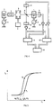
- bistable semiconductor laser under test which is a conventional single-longitudinal mode laser, connected to a generator 2 of a highly stable bias current, such as to make laser 1 operate near its threshold and act as an amplifier.
- bistable operation of a semiconductor laser is obtained by launching into said laser an optical pump signal, having a wavelength slightly different from that emitted by laser 1.
- That pump signal is generated by a second semiconductor laser 3, analogous to laser 1, connected to a respective bias current generator 4, this too highly stable.
- the systems for stabilizing the laser working temperature are not shown, since their function is of no interest for the invention.
- characterization of laser 1 exploits the laser hysteresis loop expressed by the intensity of the light outgoing from the laser as a function of the input light intensity.
- the beam generated by laser 3 is sent via an insulator 5 to an acousto-optical device 6, fed by an amplitude-modulated carrier, more particularly a carrier modulated by a sinusoidal signal.
- the aim of insulator 5 is that of preventing back-reflections which could annoy the measurement.
- Reference 7 schematises the whole of the devices generating the modulated carrier.
- the beam outgoing from acousto-optical device 6 (e.g.
- the beam deflected into the first Bragg diffracted order which has a sinusoidally varying intensity, is sent to a beam splitter 8 forming a transmitted partial beam and a reflected partial beam.
- the transmitted partial beam is sent to laser 1 under test, it is optically amplified by laser 1 and then is collected by a photodetector 9 whose output is connected, through an amplifier 10, to the y input of a memory oscilloscope 11 operated in x-y mode.
- the partial beam reflected by beam-splitter 8 is collected by a second photodetector 12 whose output is connected through an amplifier 13to the x imput of oscilloscope 11.
- the various optical systems collimating, focusing etc. the light beams have not been shown as they are of no interest to the present invention.
- Oscilloscope 11 stores the amplitude values of the signal outgoing from photodetector 9 (which are proportional to the values of intensity I2 of the beam outgoing from laser 1) as a function of the amplitude of the signal outgoing from photodetector 12 (which amplitude is proportional to intensity I1 of the beam injected into the laser itself).
- the transmission hysteresis loop of laser 1 is built up in this way.
- a data processing device 14 connected to oscilloscope 11, identifies switching points P1, P2 between the two states and, starting from values I2(P1), I1(P1), I2(P2), I1(P2) of I2 and I1 at such points, it calculates either the non-linear refractive index coefficient alone or said coefficient and other parameters characterizing the laser, more particularly the amplification factor, the finesse parameter and the wavelength difference between the emitted signal and the pump signal.
- Switching points P1, P2 can be identified either by obtaining the laser transmittivity from values I2, I1, or directly from the hysteresis loop.
- Laser transmittivity can also be exploited in a check phase, wherein at least the correctness of value n2 can be verified starting from the transmittivity maximum.
- Fig. 2 shows the hysteresis loop of I2 versus I1, and Fig. 3 transmittivity T versus I2.
- the relation is valid in the small optical signal approximation (far from gain saturation, as it occurs when using laser 1 as an amplifier) and assuming for simplicity a plane wave propagation.
- I2, I1, n0, n2 have the already-examined meaning; ⁇ 1, ⁇ 2 are the wavelengths of lasers 3 and 1, respectively; A is the amplification factor of laser 1 under resonance conditions; F is the finesse parameter of the passive cavity of length L and resonance wavelength ⁇ 2.
- Only the first peak of the curve representing relation (1) has been considered, namely the peak for which the argument of the sinus function at the denominator is 0.
- the operating condition in which such peak is exploited is easily obtained by a suitable choice of the wavelength difference between lasers 1 and 3, more particularly by exploiting the resonance wavelength ⁇ 2 of laser 1 closest to ⁇ 1: in an exemplary embodiment, wavelength ⁇ 1 and ⁇ 2 were 832.1 nm and 831.9 nm, respectively.
- the dashed area in Fig. 3 corresponds to the hysteresis loop of Fig. 2.
- switching points P1, P2 between the two stable states are to be identified and this can be made by either exploiting transmittivity T or directly starting from the hysteresis loop.
- n2 can be advantageously obtained also from the data relevant to the other switching point, and the average between the two values thus computed can be taken as actual value of n2.
- the method of identifying points P1, P2 directly from the hysteresis loop is based on the observation that such a loop presents two straight-line segments indicating the transitions from one state to the other: the starting points of such straight-line segments (with reference to the direction of variation of I1) are the two switching points.
- Processing device 14 can easily obtain, from the measured values of I2 and I1, the straight lines better approximating such portions and recognize the switching points as the points wherein the straight lines and the curve are no longer coincident.
- the method of the invention provides, besides the characterization step, a step in which there is checked the correctness of the value of n2 determined by either method described above, and possibly also of the value of A.
- the values of T are determined by exploiting the values of I1 and I2 already used to obtain the hysteresis loop, and the values of I2 and I1 where transmittivity is maximum are determined.
- the apparatus shown in Fig. 1 can be modified as shown in Fig. 4 so as to measure the power reflected by laser 1 in order to allow determination also of the single-pass gain G of the laser.
- the output signal of amplifier 13 (which is proportional to laser input power I1) is sent also to input x of a second memory oscilloscope 15 operated in x-y mode.
- the y input of oscilloscope 15 is fed, via an amplifier 16, with the output signal of a further photodetector 17 which receives, via beam splitter 8, a light signal consisting of the pump signal fraction reflected by the input face of laser 1.
- oscilloscope 15 stores the amplitude values of the output signal of detector 17, proportional to intensity I3 of the beam reflected by the laser 1, as intensity I1 of the pump signal varies.
- the reflection hysteresis loop is built, as shown in Fig. 5.
- Processing device 14 connected also to the output of oscilloscope 15, determines the angular coefficients of the straight lines which approximate the transmission and reflection hysteresis loops in the switching regions, and calculates single-pass gain G starting from such angular coefficients.
- B is a constant quantity, as r is a constant constructional parameter and G is constant under the conditions where (1) and (6) apply. Therefore, the first derivative of B with respect to I1 will be 0 whatever the point where it is calculated, and in particular in the straight-line switching regions of the hysteresis loops including switching points P1, P2.
- facet reflectivity r may be determined in a calibration phase of the equipment by measuring the power reflected by laser 1 in idle conditions.
- Value Gm may subsequently be employed to calculate A according to relation (5).
Landscapes
- Physics & Mathematics (AREA)
- General Physics & Mathematics (AREA)
- Optics & Photonics (AREA)
- Nonlinear Science (AREA)
- Condensed Matter Physics & Semiconductors (AREA)
- Electromagnetism (AREA)
- Semiconductor Lasers (AREA)
- Investigating Or Analysing Materials By Optical Means (AREA)
- Testing Of Individual Semiconductor Devices (AREA)
Claims (9)
- Méthode pour mesurer les paramètres caractéristiques d'un laser à semi-conducteur (1), polarisé par un courant qui le fait travailler comme amplificateur et amené en conditions de fonctionnement bistable par un signal optique de pompage, obtenu en modulant en amplitude un faisceau lumineux émis par un second laser à semi-conducteur (3), caractérisée en ce que: le second laser à semi-conducteur (3) travaille à une longueur d'onde, λ₁, légèrement supérieure à la longueur d'onde, λ₂, du laser testé (1); on mesure la puissance de sortie (I2) du laser testé (1) en fonction de la puissance d' entrée (I1) dudit laser, qui est faite varier, pour déterminer le cycle d'hystérésis de la puissance de sortie; on identifie les points de commutation (P1, P2) entre les deux états stables du laser testé (1) en utilisant les valeurs de puissance mesurées; on mémorise les valeurs de puissance de sortie et d'entrée [I2(P1), I1(P1), I2(P2), I1(P2)] relatifs à ces points, et on obtient la valeur du coefficient non linéaire (n2) de l'indice de réfraction du matériau employé pour la fabrication du laser testé (1) à partir des valeurs de puissance de sortie et d'entrée relatifs à un au moins de ces points (P1, P2).
- Méthode selon la revendication 1, caractérisée en ce que, pour identifier les points de commutation, on obtient le facteur de transmission, T, du laser (1) à partir des valeurs de puissance d'entrée et de sortie (I1, I2), et on compare les valeurs dudit facteur de transmission T, exprimé comme rapport entre les puissances de sortie et d'entrée (I2, I1), aux valeurs du même facteur de transmission lorsque celui-ci est exprimé en fonction des paramètres du laser, c'est-à-dire du facteur d'amplification, A, du paramètre de finesse, F, de la cavité du laser et de la différence de longueur d'onde λ₂ - λ₁ entre le laser testé (1) et le second laser (3), les points de commutation étant les points où les valeurs des dérivées premières, calculées par rapport à la puissance de sortie (I2) du laser, du facteur de transmission T exprimé 1) sous la forme de rapport entre les puissances de sortie et d'entrée et 2) en fonction des paramètres du laser, sont égales.
- Méthode selon la revendication 1, caractérisée en ce que, pour identifier les points de commutation, on détermine les valeurs de puissance d'entrée et de sortie où le cycle d'hystérésis n'a plus une allure rectiligne.
- Méthode selon l'une quelconque des revendications 1 à 3, caractérisée en ce que, en utilisant les valeurs de puissance d'entrée et de sortie relatifs aux deux points de commutation (P1, P2), on détermine aussi le facteur d'amplification, A, le paramètre de finesse, F, de la cavité du laser et la différence de longueur d'onde, λ₂ - λ₁, entre le laser testé (1) et le second laser (3).
- Méthode selon l'une quelconque des revendications qui précèdent, caractérisée en ce qu'elle comporte une phase de contrôle pour vérifier l'exactitude de la mesure du coefficient non linéaire (n2) de l'indice de réfraction, phase pendant laquelle on mesure le facteur de transmission T du laser testé (1) en fonction de la puissance de sortie (I2), on détecte le maximum de ce facteur de transmission et on obtient le coefficient non linéaire de l'indice de réfraction à partir de la valeur de puissance de sortie qui donne lieu à ce maximum.
- Méthode selon l'une quelconque des revendications qui précèdent, caractérisée en ce qu'on mesure la puissance (I3) réfléchie par le laser testé (1) en fonction de la puissance d'entrée (I1) pour déterminer le cycle d'hystérésis de la puissance réfléchie, et on détermine le gain de passage simple G du laser testé (1) à partir des valeurs de la puissance réfléchie (I3), de la puissance de sortie (I2) et de la puissance d'entrée (I1).
- Méthode selon la revendication 6, caractérisée en ce que la mesure du gain de passage simple, G, comprend les opérations de: déterminer les coefficients angulaires a(P1), b(P1), a(P2), b(P2) des lignes droites qui, dans les cycles d'hystérésis en transmission et en réflection, approchent les régions de transition entre les deux états stables du laser testé (1), les coefficients angulaires étant définis comme a(Pi) = (dI2/dI1)Pi = tangϑT(Pi), et b(Pi) = (dI3/dI1)Pi = tangϑR(Pi); calculer, à partir de ces coefficients angulaires (a, b), la valeur d'un paramètre (B) qui lie le pouvoir de réflexion (R) et le facteur de transmission (T) du laser et qui est une fonction de ce gain G; et calculer le gain G à partir de la valeur de ce paramètre B.
- Méthode selon la revendication 7, caractérisée en ce qu'on détermine une valeur moyenne Gm du gain, à partir d'une moyenne pondérée Bm de ce paramètre B, obtenue d'une valeur moyenne des coefficients angulaires des deux lignes droites qui, dans chacun desdits cycles d'hystérésis, approchent les deux régions de commutation.
- Méthode selon l'une quelconque des revendications 6 à 8 si référées à la revendication 4, caractérisée en ce qu'on calcule la valeur du facteur d'amplification A à partir du gain de passage simple G, pour contrôler la mesure basée sur le cycle d'hystérésis de la puissance de sortie.
Applications Claiming Priority (2)
| Application Number | Priority Date | Filing Date | Title |
|---|---|---|---|
| IT6747588 | 1988-05-24 | ||
| IT67475/88A IT1219324B (it) | 1988-05-24 | 1988-05-24 | Procedimento per la caratterizzazione di laser a semiconduttore ristabili |
Publications (3)
| Publication Number | Publication Date |
|---|---|
| EP0343610A2 EP0343610A2 (fr) | 1989-11-29 |
| EP0343610A3 EP0343610A3 (en) | 1990-06-27 |
| EP0343610B1 true EP0343610B1 (fr) | 1993-08-04 |
Family
ID=11302715
Family Applications (1)
| Application Number | Title | Priority Date | Filing Date |
|---|---|---|---|
| EP89109292A Expired - Lifetime EP0343610B1 (fr) | 1988-05-24 | 1989-05-23 | Méthode pour caractériser des lasers à semi-conducteur bistables |
Country Status (6)
| Country | Link |
|---|---|
| US (1) | US5007735A (fr) |
| EP (1) | EP0343610B1 (fr) |
| JP (1) | JPH0277665A (fr) |
| CA (1) | CA1321484C (fr) |
| DE (2) | DE68908013T2 (fr) |
| IT (1) | IT1219324B (fr) |
Families Citing this family (2)
| Publication number | Priority date | Publication date | Assignee | Title |
|---|---|---|---|---|
| GB8909362D0 (en) * | 1989-04-25 | 1989-06-14 | British Telecomm | High gain semiconductor laser amplifier package |
| IT1240480B (it) * | 1990-07-04 | 1993-12-17 | Cselt Centro Studi Lab Telecom | Procedimento per la misura del coefficiente non lineare dell'indice dirifrazione di un componente ottico a cavita' risonante bistabile. |
Family Cites Families (2)
| Publication number | Priority date | Publication date | Assignee | Title |
|---|---|---|---|---|
| GB8612956D0 (en) * | 1986-05-28 | 1986-07-02 | British Telecomm | Optical signal regenerator |
| GB8629871D0 (en) * | 1986-12-15 | 1987-01-28 | British Telecomm | Optical switch |
-
1988
- 1988-05-24 IT IT67475/88A patent/IT1219324B/it active
-
1989
- 1989-04-13 US US07/337,383 patent/US5007735A/en not_active Expired - Fee Related
- 1989-05-17 JP JP1121681A patent/JPH0277665A/ja active Pending
- 1989-05-23 DE DE89109292T patent/DE68908013T2/de not_active Expired - Fee Related
- 1989-05-23 DE DE198989109292T patent/DE343610T1/de active Pending
- 1989-05-23 EP EP89109292A patent/EP0343610B1/fr not_active Expired - Lifetime
- 1989-05-23 CA CA000600423A patent/CA1321484C/fr not_active Expired - Fee Related
Also Published As
| Publication number | Publication date |
|---|---|
| DE68908013D1 (de) | 1993-09-09 |
| EP0343610A2 (fr) | 1989-11-29 |
| US5007735A (en) | 1991-04-16 |
| DE68908013T2 (de) | 1994-01-05 |
| DE343610T1 (de) | 1990-09-27 |
| JPH0277665A (ja) | 1990-03-16 |
| IT8867475A0 (it) | 1988-05-24 |
| CA1321484C (fr) | 1993-08-24 |
| EP0343610A3 (en) | 1990-06-27 |
| IT1219324B (it) | 1990-05-03 |
Similar Documents
| Publication | Publication Date | Title |
|---|---|---|
| DE69602623T2 (de) | Lichtquelle für faseroptischen kreisel mit wellenlängenregelung | |
| USRE34972E (en) | Optical fiber evaluation method and system | |
| Nakamura et al. | Optical frequency domain ranging by a frequency-shifted feedback laser | |
| US8477296B2 (en) | Opto-electronic signal processing methods, systems, and apparatus for optical sensor interrogation | |
| CN105180823A (zh) | 基于锁频技术和拍频原理的光纤激光静态应变解调系统 | |
| EP0405553B1 (fr) | Réflectomètre optique à domaine de temps utilisant un élément optique à trois modes de contrôle d'oscillation, d'atténuation et d'amplification | |
| Schneider | Wavelength and line width measurement of optical sources with femtometre resolution | |
| EP0343610B1 (fr) | Méthode pour caractériser des lasers à semi-conducteur bistables | |
| EP0464798B1 (fr) | Méthode pour mesurer l'indice de réfraction non linéaire d'un composant optique avec une cavité résonante | |
| JPH07111453B2 (ja) | 半導体レーザから成るシステムのパラメータ測定方法 | |
| Kocabas et al. | Design and analysis of an integrated optical sensor for scanning force microscopies | |
| EP0194096B1 (fr) | Système pour la mesure des signaux faibles, piloté par un laser C3(cleaved-coupled-cavity) | |
| Giuliani et al. | Linewidth, autocorrelation, and cross-correlation measurements of counterpropagating modes in GaAs-AlGaAs semiconductor ring lasers | |
| US5864400A (en) | Method of and device for measuring return losses in optical fiber components | |
| US4951286A (en) | Device and method for squeezed state generation by a coupled system | |
| Andrés et al. | Optical-fiber resonant rings based on polarization-dependent couplers | |
| CN116295566B (zh) | 基于混沌瑞利散射谱互相关的温度和应变测量装置与方法 | |
| Potter et al. | A broad band signal processing technique for miniature low-finesse Fabry-Perot interferometric sensors | |
| Henning et al. | Improved method of measuring loss and phase shifts in waveguide devices | |
| Kharasov et al. | Compact narrow-linewidth lasers for distributed fiber optic sensors | |
| Calvani et al. | Characterization of a bistable semiconductor laser amplifier through the hysteresis loop | |
| Gonzalez-Marcos et al. | Laser diode bistability as sensor of optical signal parameters | |
| Muhammad et al. | MULTIWAVELENGTH BRILLOUIN FIBER LASER WITH MEASURABLE LINEWIDTH AND SIGNAL-TO-NOISE RATIO USING 0.16 pm RESOLUTION OPTICAL SPECTRUM ANALYZER | |
| De Maria et al. | All-fiber absolute interferometric sensor by a DFB frequency-modulated source | |
| Dandridge et al. | Laser noise in fibre optic interferometer sensors |
Legal Events
| Date | Code | Title | Description |
|---|---|---|---|
| PUAI | Public reference made under article 153(3) epc to a published international application that has entered the european phase |
Free format text: ORIGINAL CODE: 0009012 |
|
| AK | Designated contracting states |
Kind code of ref document: A2 Designated state(s): DE FR GB IT NL SE |
|
| PUAL | Search report despatched |
Free format text: ORIGINAL CODE: 0009013 |
|
| ITCL | It: translation for ep claims filed |
Representative=s name: CSELT S.P.A. |
|
| AK | Designated contracting states |
Kind code of ref document: A3 Designated state(s): DE FR GB IT NL SE |
|
| 17P | Request for examination filed |
Effective date: 19900626 |
|
| EL | Fr: translation of claims filed | ||
| DET | De: translation of patent claims | ||
| TCNL | Nl: translation of patent claims filed | ||
| 17Q | First examination report despatched |
Effective date: 19920423 |
|
| GRAA | (expected) grant |
Free format text: ORIGINAL CODE: 0009210 |
|
| ITF | It: translation for a ep patent filed | ||
| AK | Designated contracting states |
Kind code of ref document: B1 Designated state(s): DE FR GB IT NL SE |
|
| REF | Corresponds to: |
Ref document number: 68908013 Country of ref document: DE Date of ref document: 19930909 |
|
| ET | Fr: translation filed | ||
| PGFP | Annual fee paid to national office [announced via postgrant information from national office to epo] |
Ref country code: SE Payment date: 19940506 Year of fee payment: 6 |
|
| PGFP | Annual fee paid to national office [announced via postgrant information from national office to epo] |
Ref country code: GB Payment date: 19940513 Year of fee payment: 6 |
|
| PGFP | Annual fee paid to national office [announced via postgrant information from national office to epo] |
Ref country code: FR Payment date: 19940530 Year of fee payment: 6 |
|
| PGFP | Annual fee paid to national office [announced via postgrant information from national office to epo] |
Ref country code: NL Payment date: 19940531 Year of fee payment: 6 Ref country code: DE Payment date: 19940531 Year of fee payment: 6 |
|
| PLBE | No opposition filed within time limit |
Free format text: ORIGINAL CODE: 0009261 |
|
| STAA | Information on the status of an ep patent application or granted ep patent |
Free format text: STATUS: NO OPPOSITION FILED WITHIN TIME LIMIT |
|
| 26N | No opposition filed | ||
| EAL | Se: european patent in force in sweden |
Ref document number: 89109292.6 |
|
| PG25 | Lapsed in a contracting state [announced via postgrant information from national office to epo] |
Ref country code: GB Effective date: 19950523 |
|
| PG25 | Lapsed in a contracting state [announced via postgrant information from national office to epo] |
Ref country code: SE Effective date: 19950524 |
|
| PG25 | Lapsed in a contracting state [announced via postgrant information from national office to epo] |
Ref country code: NL Effective date: 19951201 |
|
| GBPC | Gb: european patent ceased through non-payment of renewal fee |
Effective date: 19950523 |
|
| NLV4 | Nl: lapsed or anulled due to non-payment of the annual fee |
Effective date: 19951201 |
|
| PG25 | Lapsed in a contracting state [announced via postgrant information from national office to epo] |
Ref country code: DE Effective date: 19960201 |
|
| EUG | Se: european patent has lapsed |
Ref document number: 89109292.6 |
|
| PG25 | Lapsed in a contracting state [announced via postgrant information from national office to epo] |
Ref country code: FR Effective date: 19960229 |
|
| REG | Reference to a national code |
Ref country code: FR Ref legal event code: ST |
|
| REG | Reference to a national code |
Ref country code: FR Ref legal event code: ST |
|
| PG25 | Lapsed in a contracting state [announced via postgrant information from national office to epo] |
Ref country code: IT Free format text: LAPSE BECAUSE OF NON-PAYMENT OF DUE FEES;WARNING: LAPSES OF ITALIAN PATENTS WITH EFFECTIVE DATE BEFORE 2007 MAY HAVE OCCURRED AT ANY TIME BEFORE 2007. THE CORRECT EFFECTIVE DATE MAY BE DIFFERENT FROM THE ONE RECORDED. Effective date: 20050523 |