EP0343392B1 - Arrangement for displaying a variable quantity from a driven semiconductor - Google Patents
Arrangement for displaying a variable quantity from a driven semiconductor Download PDFInfo
- Publication number
- EP0343392B1 EP0343392B1 EP89107538A EP89107538A EP0343392B1 EP 0343392 B1 EP0343392 B1 EP 0343392B1 EP 89107538 A EP89107538 A EP 89107538A EP 89107538 A EP89107538 A EP 89107538A EP 0343392 B1 EP0343392 B1 EP 0343392B1
- Authority
- EP
- European Patent Office
- Prior art keywords
- input
- comparator
- arrangement according
- constructed
- component
- Prior art date
- Legal status (The legal status is an assumption and is not a legal conclusion. Google has not performed a legal analysis and makes no representation as to the accuracy of the status listed.)
- Expired - Lifetime
Links
Images

Classifications
-
- G—PHYSICS
- G01—MEASURING; TESTING
- G01R—MEASURING ELECTRIC VARIABLES; MEASURING MAGNETIC VARIABLES
- G01R19/00—Arrangements for measuring currents or voltages or for indicating presence or sign thereof
- G01R19/0007—Frequency selective voltage or current level measuring
- G01R19/0015—Frequency selective voltage or current level measuring separating AC and DC
-
- G—PHYSICS
- G01—MEASURING; TESTING
- G01R—MEASURING ELECTRIC VARIABLES; MEASURING MAGNETIC VARIABLES
- G01R15/00—Details of measuring arrangements of the types provided for in groups G01R17/00 - G01R29/00, G01R33/00 - G01R33/26 or G01R35/00
- G01R15/14—Adaptations providing voltage or current isolation, e.g. for high-voltage or high-current networks
- G01R15/18—Adaptations providing voltage or current isolation, e.g. for high-voltage or high-current networks using inductive devices, e.g. transformers
- G01R15/183—Adaptations providing voltage or current isolation, e.g. for high-voltage or high-current networks using inductive devices, e.g. transformers using transformers with a magnetic core
- G01R15/185—Adaptations providing voltage or current isolation, e.g. for high-voltage or high-current networks using inductive devices, e.g. transformers using transformers with a magnetic core with compensation or feedback windings or interacting coils, e.g. 0-flux sensors
Definitions
- the invention relates to an arrangement for emulating an alternating variable, which has a direct component, in particular an alternating current, in a controlled semiconductor component with an electromagnetic transducer for measurement purposes.
- the invention has for its object to provide an arrangement of the type mentioned, with a controlled Semiconductor component, the electrical alternating variable with the same component can be simulated in a simple manner for measuring, regulating and control functions.
- a secondary winding of the converter is connected to an input of a sample and hold element, the trigger input of which is connected to a control device for the semiconductor component and trigger pulses from this control device in each case receives the control times of the semiconductor component, and that the output of the sample and hold element, whose output signal is proportional to the DC component, is routed to a first input of a comparator, the second input of which is connected to the secondary winding of the converter and at whose output the reproduced variable size is available.
- the comparator is a subtractor, the first input being designed as an inverting input and the second input as a non-inverting input.
- the simulated alternating variable also corresponds in its phase position to the original alternating variable.
- the inverting element and / or the comparator are preferably designed as amplifiers. An adjustment of the level relationships between the converter and the subsequent elements can thus be achieved, whereby the detection of even very small DC components is possible.
- a filter arrangement is arranged between the output of the comparator and a measuring output, which is designed as a blocking and low-pass filter.
- a measuring output which is designed as a blocking and low-pass filter.
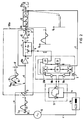
- FIG. 1 shows an arrangement 100 for emulating an alternating variable in a controlled semiconductor component, in particular a thyristor.
- a thyristor actuator 13 which forms a circuit with lines a, b, c, a load 14 and a voltage source 15.
- a current I T flows through the actuator 13 as shown. It should be noted that the two half-waves have different sizes due to unequal firing angles and therefore the current curve has a DC component. This should be stationary.
- the semiconductor components 1 of the actuator 13 receive their control pulses from a control device 2.
- This control device 2 includes a pulse generator 24, the output pulses of which are passed on to the controlled semiconductors 1 via angle controls 23a, 23b and adaptation stages 18a, 18b.
- the current I T is detected by a converter 3.
- a voltage U W is transmitted as shown on its secondary side on the line d. It can be seen that the DC component is suppressed by the converter 3. The voltage time areas of the associated positive and negative half-waves are the same size. The original zero line 16 of the current profile I T is shifted downward by the amount 17 of the DC component.
- This voltage U W is fed via line d to an input 5 of a sample & hold element 4, the trigger input 6 of which is coupled to the control device 2. From the control device 2, the sample & hold element 4 receives trigger pulses each at the control times 20 of the semiconductor components 1.
- the comparator 9 is designed as a subtractor, the first input 8a being designed as an inverting input and the second input 8b as a non-inverting input. This means that the constant component U GL is subtracted from the alternating variable U W.
- the comparator 9 is the in-phase replica U IT of the original Change size I T on.
- the signal U IT is then used for further measurement purposes. It can be passed on, for example, to temperature monitors, monitoring and control devices or, as shown, to a measuring device 25 which displays the current value.
- FIG. 2 shows a further exemplary embodiment of the.
- the comparator 9 is designed as a summing element. So that the DC component with the correct polarity is summed with the converter signal, an inverting element 10 is arranged between the sample and hold element 4 and the comparator 9. Alternatively, an inverting element 10a can also be arranged at the input of the sample & hold element 4.
- the inverting element 10, 10a and / or the comparator 9 are preferably designed as amplifiers in order to achieve an optimal adaptation of the individual elements to one another.
- a filter 12 is arranged between the output 21 of the comparator 9 and a measuring output 22 and is designed as a blocking and low-pass filter. All alternating components of the voltage U IT are eliminated by the filter 12, so that a voltage U F is present at the measuring output 22 which is proportional to the entire DC component contained in the current I T. This can be routed, for example, via a line f to a control unit 19 of the control device 2 in order to achieve an undesired DC component in the load circuit by correcting the control times. This is of particular importance when the load 14 is inductive and an undesirable bias occurs.
- the voltage U F serves as a measure of the premagnetization. Alternatively, the voltage can also be supplied to monitoring devices or, as shown, to a measuring device 25a.
- An essential advantage of the arrangement 100 or 100a is that only the same component is detected by the sample and hold element 4, which is not transmitted by the converter 3. This means that, for example, briefly dynamically occurring components that the converter 3 can be transmitted, not detected by the sample and hold element 4. In contrast to the signal U W, they have no shift in the alternating variable on the secondary side of the converter 3 over time. Dynamic components are therefore specifically taken into account and, if necessary, can be treated further in the filter arrangement 12.
Landscapes
- Engineering & Computer Science (AREA)
- Power Engineering (AREA)
- Physics & Mathematics (AREA)
- General Physics & Mathematics (AREA)
- Measurement Of Current Or Voltage (AREA)
- Power Conversion In General (AREA)
- Rectifiers (AREA)
Description
Die Erfindung betrifft eine Anordnung zum Nachbilden einer Wechselgröße, die eine Gleichkomponente aufweist, insbesondere eines Wechselstromes, bei einem gesteuerten Halbleiter-Bauelement mit einem elektromagnetischen Wandler für Meßzwecke.The invention relates to an arrangement for emulating an alternating variable, which has a direct component, in particular an alternating current, in a controlled semiconductor component with an electromagnetic transducer for measurement purposes.
Beim Übertragen einer Wechselgröße mittels eines elektromagnetischen Wandlers wird eine stationäre Gleichkomponente nicht übertragen. Die Folge ist eine Nullpunktsverschiebung der vom Wandler abgegebenen Wechselgröße gegenüber der Eingangswechselgröße. Diese Problematik tritt insbesondere bei der Messung von Strömen bei gesteuerten Halbleiter-Bauelementen auf. Es kann z.B. eine Gleichkomponente im Stromverlauf eines Thyristorstellers durch ungleiche Zündwinkel für die einzelnen Thyristoren auftreten. Da die gemessene Wechselgröße für die Thyristorsteuerung benötigt wird, ist es besonders wichtig, einen unverfälschten Wert zu erhalten.When an alternating variable is transmitted by means of an electromagnetic converter, a stationary DC component is not transmitted. The result is a zero point shift of the alternating variable output by the converter compared to the input alternating variable. This problem arises in particular when measuring currents in the case of controlled semiconductor components. For example, a DC component in the current curve of a thyristor controller due to unequal firing angles for the individual thyristors. Since the measured alternating variable is required for thyristor control, it is particularly important to obtain an unadulterated value.
Dazu wurden bisher Einrichtungen eingesetzt, (vge. z.B. US-A-4255704), die infolge besonderer Vorkehrungen eine Gleichkomponente übertragen können. Diese Einrichtungen enthalten z.B. Wandler mit einer besonderen Zusatzwicklung, über die eine Vormagnetisierung des Wandlerkerns bewirkt wird, die der Magnetisierung infolge der Gleichkomponente entgegenwirkt. Solche Wandler sind aufwendig. Außerdem sind hierbei zusätzliche Regeleinrichtungen für die Vormagnetisierung erforderlich.Up to now, devices have been used for this (vge. E.g. US-A-4255704), which can transmit a DC component due to special precautions. These facilities include e.g. Transducers with a special additional winding, via which a pre-magnetization of the transducer core is effected, which counteracts the magnetization due to the DC component. Such converters are expensive. In addition, additional control devices for the premagnetization are required.
Der Erfindung liegt die Aufgabe zugrunde, eine Anordnung der eingangs genannten Art anzugegeben, mit der bei einem gesteuerten Halbleiter-Bauelement die elekrische Wechselgröße mit Gleichkomponente auf einfache Art für Meß-, Regel- und Steuerfunktionen nachgebildet werden kann.The invention has for its object to provide an arrangement of the type mentioned, with a controlled Semiconductor component, the electrical alternating variable with the same component can be simulated in a simple manner for measuring, regulating and control functions.
Diese Aufgabe wird bei einer Anordnung der eingangs genannten Art erfindungsgemäß dadurch gelöst, daß eine Sekundärwicklung des Wandlers mit einem Eingang eines Sample & Hold-Gliedes verbunden ist, dessen Triggereingang an eine Steuereinrichtung für das Halbleiter-Bauelement angeschlossen ist und von dieser Steuereinrichtung Triggerimpulse jeweils zu den Steuerzeitpunkten des Halbleiter-Bauelementes erhält, und daß der Ausgang des Sample & Hold-Gliedes, dessen Ausgangssignal proportional der Gleichkomponente ist, auf einen ersten Eingang eines Vergleichers geführt ist, dessen zweiter Eingang mit der Sekundärwicklung des Wandlers verbunden ist und an dessen Ausgang die nachgebildete Wechselgröße abgreifbar ist.This object is achieved according to the invention in an arrangement of the type mentioned at the outset in that a secondary winding of the converter is connected to an input of a sample and hold element, the trigger input of which is connected to a control device for the semiconductor component and trigger pulses from this control device in each case receives the control times of the semiconductor component, and that the output of the sample and hold element, whose output signal is proportional to the DC component, is routed to a first input of a comparator, the second input of which is connected to the secondary winding of the converter and at whose output the reproduced variable size is available.
Auf diese Weise wird mit einfachen Mitteln eine Nachbildung der benötigten elektrischen Wechselgröße samt Gleichkomponente erreicht. Es können herkömmliche kostengünstige Wandler, z.B. übliche Schutzwandler, für die Meßwerterfassung eingesetzt werden. Diese tragen zudem durch ihre geringe Baugröße zu einer wesentlichen Verringerung des Platzbedarfs gegenüber der herkömmlichen Lösung mit Zusatzwicklung bei. Mit der vorliegenden Anordnung ist es möglich, sehr kleine Gleichstromkomponenten zu erfassen. Dabei werden nur die Gleichstromkomponenten berücksichtigt, die stationär sind und nicht vom Wandler übertragen werden.In this way, a simulation of the required electrical alternating variable including the same component is achieved with simple means. Conventional inexpensive transducers, e.g. Conventional protective transformers are used for data acquisition. Due to their small size, they also contribute to a significant reduction in space requirements compared to the conventional solution with additional winding. With the present arrangement it is possible to detect very small direct current components. Only the DC components that are stationary and are not transmitted by the converter are taken into account.
Es ist günstig, den Vergleicher als Subtrahierer auszubilden, wobei der erste Eingang als invertierender und der zweite Eingang als nicht-invertierender Eingang ausgebildet sind. Auf diese Weise entspricht die nachgebildete Wechselgröße (Gleich- und Wechselkomponente) auch in ihrer Phasenlage der ursprünglichen Wechselgröße. Dieser Vorteil ist ebenfalls bei einer Ausführung gegeben, bei der der Vergleicher als Summierglied aus gebildet und zwischen dem Sample & Hold-Glied und dem Vergleicher ein Invertierglied angeordnet ist.It is expedient to design the comparator as a subtractor, the first input being designed as an inverting input and the second input as a non-inverting input. In this way, the simulated alternating variable (equal and alternating component) also corresponds in its phase position to the original alternating variable. This advantage is also given in an embodiment in which the comparator is a summing element formed and an inverting element is arranged between the sample and hold element and the comparator.
Vorzugsweise sind das Invertierglied und/oder der Vergleicher als Verstärker ausgebildet. Damit kann eine Anpassung der Pegelverhältnisse zwischen dem Wandler und den nachfolgenden Gliedern erzielt werden, wodurch die Erfassung auch sehr kleine Gleichkomponenten möglich ist.The inverting element and / or the comparator are preferably designed as amplifiers. An adjustment of the level relationships between the converter and the subsequent elements can thus be achieved, whereby the detection of even very small DC components is possible.
Nach einer vorteilhaften Ausgestaltung ist zwischen dem Ausgang des Vergleichers und einem Meßausgang eine Filteranordnung angeordnet, die als Sperr- und Tiefpaß-Filter ausgebildet ist. So steht am Meßausgang die gesamte in der Wechselgröße enthaltene Gleichkomponente für weitere Zwecke zur Verfügung. Dieses Meßsignal kann mit Vorteil dazu dienen, über die Steuereinrichtung eine Ausregelung der unerwünschten Gleichkomponente zu erzielen.According to an advantageous embodiment, a filter arrangement is arranged between the output of the comparator and a measuring output, which is designed as a blocking and low-pass filter. Thus, the entire DC component contained in the alternating variable is available for further purposes at the measurement output. This measurement signal can advantageously be used to control the undesired DC component via the control device.
Weitere vorteilhafte Ausgestaltungen sind in den Unteransprüchen angegeben.Further advantageous refinements are specified in the subclaims.
Ausführungsbeispiele der erfindungsgemäßen Anordnung werden anhand der Zeichnung im folgenden näher erläutert. Es zeigen:
- FIG 1 eine erste Anordnung zum Nachbilden des Wechselstromes an einem Thyristor-Stellglied und
- FIG 2 eine zweite solche Anordnung.
- 1 shows a first arrangement for emulating the alternating current on a thyristor actuator and
- 2 shows a second such arrangement.
In FIG 1 ist eine Anordnung 100 zum Nachbilden einer Wechselgröße bei einem gesteuerten Halbleiter-Bauelement, insbesondere einem Thyristor,gezeigt. Dieser ist Bestandteil eines Thyristor-Stellgliedes 13, das mit Leitungen a, b, c, einer Last 14 und einer Spannungsquelle 15 einen Stromkreis bildet. Durch das Stellglied 13 fließt ein Strom IT wie dargestellt. Dabei ist zu beachten, daß die beiden Halbwellen aufgrund ungleicher Zündwinkel unterschiedliche Größe haben und der Stromverlauf daher eine Gleichkomponente aufweist. Diese soll stationär sein. Die Halbleiter-Bauelemente 1 des Stellgliedes 13 erhalten ihre Steuerimpulse aus einer Steuereinrichtung 2. Diese Steuereinrichtung 2 beinhaltet einen Impulsgenerator 24, dessen Ausgangsimpulse über Winkelsteuerungen 23a, 23b und Anpassungsstufen 18a, 18b an die gesteuerten Halbleiter 1 weitergeben werden. Der Strom IT wird von einem Wandler 3 erfaßt. Durch die Übertragungseigenschaften des Wandlers 3 wird auf seine Sekundärseite auf der Leitung d eine Spannung UW wie dargestellt übertragen. Man erkennt, daß die Gleichkomponente vom Wandler 3 unterdrückt ist. Die Spannungszeitflächen der zueinander zugehörigen positiven und negativen Halbwellen sind gleich groß. Die ursprüngliche Nullinie 16 des Stromverlaufs IT ist um den Betrag 17 der Gleichkomponente nach unten verschoben. Diese Spannung UW wird über Leitung d auf einen Eingang 5 eines Sample & Hold-Gliedes 4 gegeben, dessen Triggereingang 6 mit der Steuereinrichtung 2 gekoppelt ist. Von der Steuereinrichtung 2 erhält das Sample & Hold-Glied 4 Triggerimpule jeweils zu den Steuerzeitpunkten 20 der Halbleiter-Bauelemente 1. Dadurch wird erzielt, daß jeweils zu den Steuerzeitpunkten 20 der Halbleiter-Bauelemente 1 die Spannung UW abgetastet wird und dieser Wert solange am Ausgang 7 des Sample & Hold-Gliedes 4 ausgegeben wird, bis ein nächster Triggerimpuls folgt. Zum Steuerzeitpunkt 20 ist der Strom IT der Halbleiter-Bauelemente 1 Null. Betrachtet man zu diesen Zeitpunkten 20 den Wert der Spannung UW, so erhält man genau mit dem Betrag 17 den Anteil der Gleichkomponente. Das Ausgangssignal UGL auf Leitung e des Sample & Hold-Gliedes 4 ist also proportional der Gleichkomponente. Der Ausgang 7 ist mit einem ersten Eingang 8a eines Vergleichers 9 verbunden, dessen zweiter Eingang 8b mit der Sekundärwicklung des Wandlers 3 verbunden ist. Dabei ist es günstig, daß der Vergleicher 9 als Subtrahierer ausgebildet ist, wobei der erste Eingang 8a als invertierender und der zweite Eingang 8b als nicht-invertierender Eingang ausgebildet sind. Das bedeutet, daß die Gleichkomponente UGL von der Wechselgröße UW subtrahiert wird. Am Ausgang 21 des Vergleichers 9 steht so die phasenrichtige Nachbildung UIT der ursprünglichen Wechselgröße IT an. Das Signal UIT wird dann für weitere Meßzwecke verwendet. Es kann z.B. an Temperaturüberwachungen, Überwachungs -und Regeleinrichtungen oder wie dargestellt, an eine Meßeinrichtung 25 weitergegeben werden, die den Stromwert anzeigt.1 shows an
In FIG 2 ist ein weiteres Ausführungsbeispiel der dargestellt. Dabei ist der Vergleicher 9 als Summierglied ausgebildet. Damit die Gleichkomponente mit der richtigen Polarität mit dem Wandlersignal summiert wird, ist zwischen dem Sample & Hold-Glied 4 und dem Vergleicher 9 ein Invertierglied 10 angeordnet. Alternativ kann auch ein Invertierglied 10a am Eingang des Sample & Hold-Gliedes 4 angeordnet sein. Das Invertierglied 10, 10a und/oder der Vergleicher 9 sind vorzugsweise als Verstärker ausgebildet, um eine optimale Anpassung der einzelnen Glieder aufeinander zu erzielen.FIG. 2 shows a further exemplary embodiment of the. The
Zwischem dem Ausgang 21 des Vergleichers 9 und einem Meßausgang 22 ist ein Filter 12 angeordnet, das als Sperr- und Tiefpassfilter ausgebildet ist. Durch das Filter 12 werden alle Wechselanteile der Spannung UIT eliminiert, so daß am Meßausgang 22 eine Spannung UF ansteht, die der gesamten im Strom IT enthaltenen Gleichkomponente proportional ist. Diese kann beispielsweise über eine Leitung f auf ein Steuergerät 19 der Steuereinrichtung 2 geführt werden, um durch eine Korrektur der Steuerzeitpunkte eine unerwünschte Gleichkomponente im Laststromkreis zu erzielen. Dies ist von besonderer Bedeutung, wenn die Last 14 induktiv ist und eine unerwünschte Vormagnetisierung auftritt. Die Spannung UF dient als ein Maß für die Vormagnetisierung. Alternativ kann die Spannung auch Überwachungseinrichtungen oder wie dargestellt, einer Meßeinrichtung 25a zugeführt werden.A
Wesentlicher Vorteil der Anordnung 100 bzw. 100a ist, daß nur die Gleichkomponente von dem Sample & Hold-Glied 4 erfaßt wird, die von dem Wandler 3 nicht übertragen wird. Das heißt, daß z.B. kurzzeitig dynamisch auftretende Komponenten, die der Wandler 3 übertragen kann, von dem Sample & Hold-Glied 4 nicht erfaßt werden. Sie weisen im zeitlichen Verlauf im Gegensatz zum Signal UW keine Verschiebung der Wechselgröße auf der Sekundärseite des Wandlers 3 auf. Dynamische Komponenten werden also speziell berücksichtigt und können gegebenenfalls in der Filteranordnung 12 weiter behandelt werden.An essential advantage of the
Claims (10)
- Arrangement for the reproduction of an alternating quantity, which has a direct component, in particular of an alternating current in a controlled semiconductor component (1), with a measuring electromagnetic transformer (3), characterized in that a secondary winding of the transformer (3) is connected to an input (5) of a sample and hold circuit (4), the trigger input (6) of which is attached to a control device (2) for the semiconductor component (1) and from this control device (2) receives trigger pulses in each case at the control instants (20) of the semiconductor component (1), and in that the output (7) of the sample and hold circuit (4), the output signal of which is proportional to the direct component, is conducted to a first input (8a) of a comparator (9), the second input (8b) of which is connected to the secondary winding of the transformer (3) and at the output (21) of which the reproduced alternating quantity can be picked up.
- Arrangement according to claim 1, characterized in that the comparator (9) is constructed as a subtractor with a first and second input, and in that the first input (8a) is constructed as an inverting input and the second input (8b) is constructed as a non-inverting input.
- Arrangement according to claim 1, characterized in that the comparator (9) is constructed as a summing element and in that an inverting element (10) is arranged between the sample & hold element (4) and the comparator (9).
- Arrangement according to claim 1, characterized in that the comparator (9) is constructed as a summing element, and in that an inverting element (10a) is arranged at the input (5) of the sample & hold element (4).
- Arrangement according to claim 3 or 4, characterized in that the inverting element (10, 10a) is constructed as an amplifier.
- Arrangement according to one of the preceding claims, characterized in that between the output (21) of the comparator (9) and a measuring output (22), at which the reproduced alternating quantity can be picked up, a filter (12) is arranged, which is constructed as a blocking and low-pass filter.
- Arrangement according to one of the preceding claims, characterized in that the comparator (9) is constructed as an amplifier.
- Arrangement according to one of claims 1 to 7, characterized in that the semiconductor component (1) comprises at least one thyristor.
- Arrangement according to claim 8, characterized in that the semiconductor component (1) is a component of a thyristor control device (13).
- Arrangement according to one of claims 6 to 9, characterized in that a measuring device (25, 25a) is attached to the measuring output (22), which measuring device displays a current value.
Applications Claiming Priority (2)
| Application Number | Priority Date | Filing Date | Title |
|---|---|---|---|
| DE3815849 | 1988-05-09 | ||
| DE3815849 | 1988-05-09 |
Publications (3)
| Publication Number | Publication Date |
|---|---|
| EP0343392A2 EP0343392A2 (en) | 1989-11-29 |
| EP0343392A3 EP0343392A3 (en) | 1989-12-06 |
| EP0343392B1 true EP0343392B1 (en) | 1992-09-23 |
Family
ID=6354011
Family Applications (1)
| Application Number | Title | Priority Date | Filing Date |
|---|---|---|---|
| EP89107538A Expired - Lifetime EP0343392B1 (en) | 1988-05-09 | 1989-04-26 | Arrangement for displaying a variable quantity from a driven semiconductor |
Country Status (5)
| Country | Link |
|---|---|
| US (1) | US4904925A (en) |
| EP (1) | EP0343392B1 (en) |
| JP (1) | JPH01320474A (en) |
| CA (1) | CA1313224C (en) |
| DE (1) | DE58902321D1 (en) |
Families Citing this family (2)
| Publication number | Priority date | Publication date | Assignee | Title |
|---|---|---|---|---|
| DE69221644T2 (en) * | 1991-01-08 | 1998-02-12 | Canon Kk | Electrical power supply |
| FR2870351B1 (en) * | 2004-05-14 | 2006-07-14 | Alstom Transport Sa | ELECTROMAGNETIC FIELD MEASURING DEVICE, CONTROL SYSTEM USING THE SAME, AND ELECTRONIC CIRCUIT DESIGNED THEREFOR |
Family Cites Families (6)
| Publication number | Priority date | Publication date | Assignee | Title |
|---|---|---|---|---|
| US28851A (en) * | 1860-06-26 | Improvement in sewing-machines | ||
| AU521914B2 (en) * | 1978-02-28 | 1982-05-06 | Tokyo Shibaura Denki Kabushiki Kaisha | Controlling electric valves in ac power supply |
| US4278940A (en) * | 1979-04-25 | 1981-07-14 | General Electric Company | Means for automatically compensating DC magnetization in a transformer |
| US4255705A (en) * | 1979-09-24 | 1981-03-10 | General Electric Company | Peak detection and electronic compensation of D. C. saturation magnetization in current transformers used in watt hour meter installations |
| US4255704A (en) * | 1979-10-01 | 1981-03-10 | General Electric Company | Zero crossing detection and electronic compensation of D. C. saturation magnetization in current transformers used in watthour meter installations |
| DD250051A1 (en) * | 1986-06-19 | 1987-09-30 | Medizin Labortechnik Veb K | METHOD AND CIRCUIT FOR THE AUTOMATIC ZERO-POINT CORRECTION OF CLOCK-CONTROLLED MEASURING SYSTEMS |
-
1989
- 1989-04-26 DE DE8989107538T patent/DE58902321D1/en not_active Expired - Fee Related
- 1989-04-26 EP EP89107538A patent/EP0343392B1/en not_active Expired - Lifetime
- 1989-05-02 JP JP1113547A patent/JPH01320474A/en active Pending
- 1989-05-02 US US07/346,478 patent/US4904925A/en not_active Expired - Fee Related
- 1989-05-05 CA CA000598777A patent/CA1313224C/en not_active Expired - Fee Related
Also Published As
| Publication number | Publication date |
|---|---|
| JPH01320474A (en) | 1989-12-26 |
| EP0343392A3 (en) | 1989-12-06 |
| DE58902321D1 (en) | 1992-10-29 |
| US4904925A (en) | 1990-02-27 |
| CA1313224C (en) | 1993-01-26 |
| EP0343392A2 (en) | 1989-11-29 |
Similar Documents
| Publication | Publication Date | Title |
|---|---|---|
| EP0172402B1 (en) | Circuit for the fluctuation compensation of the transfer factor of a magnetic-field sensor | |
| DE3854702T2 (en) | ALYSATOR FOR ANALYZING HIGH-RESISTANCE FAULTS IN AN ELECTRICAL POWER SUPPLY NETWORK. | |
| DE4230939C2 (en) | Circuit arrangement for changing or testing electrical properties of a current transformer with magnetic field compensation | |
| DE29506883U1 (en) | Current sensor based on the compensation principle | |
| EP0386604A2 (en) | Static electricity meter | |
| EP1664804B1 (en) | Method and device for measuring voltage | |
| DE3531869A1 (en) | ELECTROMAGNETIC FLOW METER | |
| EP0022992A1 (en) | Surveillance apparatus for a battery of condensators in a direct current filtering circuit | |
| EP0150814A2 (en) | Digital impedance relay | |
| DE3779749T2 (en) | CIRCUIT TO MEASURE THE PRIMARY DEVELOPMENT OF THE OUTPUT TRANSFORMER OF A INVERTER THROUGH FLOWING DC COMPONENTS. | |
| DE68904743T2 (en) | METHOD FOR DETECTING ELECTRIC SIZES. | |
| EP0343392B1 (en) | Arrangement for displaying a variable quantity from a driven semiconductor | |
| EP0380937A1 (en) | Inductive-flow meter | |
| EP0686850A1 (en) | DC current measuring circuit with voltage isolation between current path and measuring circuit | |
| EP0250028A2 (en) | Circuit device for compensation of temperature dependent and temperature independent drifts of a capacitive sensor | |
| DE2716605C2 (en) | Circuit arrangement for earth fault detection in a converter | |
| DE4142342C2 (en) | Method and device for digital current measurement | |
| DE2261953A1 (en) | CURRENT TRANSFORMER FOR MEASURING CURRENT LEVELS, IN PARTICULAR IN HIGH VOLTAGE LINES | |
| DE2460773B2 (en) | Controllable converter circuit | |
| DE4403077C2 (en) | Circuit arrangement for an AC converter and method for operation | |
| DE2801684C3 (en) | Measuring circuit for determining the size of signal alternating voltages | |
| DE2329254A1 (en) | CURRENT CONVERTER WITH ACTIVE LOAD SHUTTER | |
| DE19538754A1 (en) | Primary line monitoring method for alarm system | |
| DE4318502C1 (en) | Method and circuit for monitoring the currents from power capacitors for power-factor correction | |
| DE2702666B2 (en) | Circuit arrangement for monitoring the phase currents in multi-phase networks |
Legal Events
| Date | Code | Title | Description |
|---|---|---|---|
| PUAI | Public reference made under article 153(3) epc to a published international application that has entered the european phase |
Free format text: ORIGINAL CODE: 0009012 |
|
| PUAL | Search report despatched |
Free format text: ORIGINAL CODE: 0009013 |
|
| AK | Designated contracting states |
Kind code of ref document: A2 Designated state(s): CH DE FR GB LI SE |
|
| AK | Designated contracting states |
Kind code of ref document: A3 Designated state(s): CH DE FR GB LI SE |
|
| 17P | Request for examination filed |
Effective date: 19900509 |
|
| 17Q | First examination report despatched |
Effective date: 19920226 |
|
| GRAA | (expected) grant |
Free format text: ORIGINAL CODE: 0009210 |
|
| AK | Designated contracting states |
Kind code of ref document: B1 Designated state(s): CH DE FR GB LI SE |
|
| REF | Corresponds to: |
Ref document number: 58902321 Country of ref document: DE Date of ref document: 19921029 |
|
| GBT | Gb: translation of ep patent filed (gb section 77(6)(a)/1977) | ||
| ET | Fr: translation filed | ||
| PG25 | Lapsed in a contracting state [announced via postgrant information from national office to epo] |
Ref country code: LI Effective date: 19930430 Ref country code: CH Effective date: 19930430 |
|
| PLBE | No opposition filed within time limit |
Free format text: ORIGINAL CODE: 0009261 |
|
| STAA | Information on the status of an ep patent application or granted ep patent |
Free format text: STATUS: NO OPPOSITION FILED WITHIN TIME LIMIT |
|
| 26N | No opposition filed | ||
| PG25 | Lapsed in a contracting state [announced via postgrant information from national office to epo] |
Ref country code: FR Effective date: 19931229 |
|
| REG | Reference to a national code |
Ref country code: CH Ref legal event code: PL |
|
| REG | Reference to a national code |
Ref country code: FR Ref legal event code: ST |
|
| EAL | Se: european patent in force in sweden |
Ref document number: 89107538.4 |
|
| PGFP | Annual fee paid to national office [announced via postgrant information from national office to epo] |
Ref country code: SE Payment date: 19960410 Year of fee payment: 8 |
|
| PG25 | Lapsed in a contracting state [announced via postgrant information from national office to epo] |
Ref country code: SE Effective date: 19970427 |
|
| PGFP | Annual fee paid to national office [announced via postgrant information from national office to epo] |
Ref country code: DE Payment date: 19970617 Year of fee payment: 9 |
|
| EUG | Se: european patent has lapsed |
Ref document number: 89107538.4 |
|
| PGFP | Annual fee paid to national office [announced via postgrant information from national office to epo] |
Ref country code: GB Payment date: 19980310 Year of fee payment: 10 |
|
| PG25 | Lapsed in a contracting state [announced via postgrant information from national office to epo] |
Ref country code: DE Free format text: LAPSE BECAUSE OF NON-PAYMENT OF DUE FEES Effective date: 19990202 |
|
| PG25 | Lapsed in a contracting state [announced via postgrant information from national office to epo] |
Ref country code: GB Free format text: LAPSE BECAUSE OF NON-PAYMENT OF DUE FEES Effective date: 19990426 |
|
| GBPC | Gb: european patent ceased through non-payment of renewal fee |
Effective date: 19990426 |