EP0342503A2 - SCR regulator for a television apparatus - Google Patents
SCR regulator for a television apparatus Download PDFInfo
- Publication number
- EP0342503A2 EP0342503A2 EP89108399A EP89108399A EP0342503A2 EP 0342503 A2 EP0342503 A2 EP 0342503A2 EP 89108399 A EP89108399 A EP 89108399A EP 89108399 A EP89108399 A EP 89108399A EP 0342503 A2 EP0342503 A2 EP 0342503A2
- Authority
- EP
- European Patent Office
- Prior art keywords
- voltage
- coupled
- supply
- inductance
- source
- Prior art date
- Legal status (The legal status is an assumption and is not a legal conclusion. Google has not performed a legal analysis and makes no representation as to the accuracy of the status listed.)
- Ceased
Links
Images
Classifications
-
- H—ELECTRICITY
- H04—ELECTRIC COMMUNICATION TECHNIQUE
- H04N—PICTORIAL COMMUNICATION, e.g. TELEVISION
- H04N3/00—Scanning details of television systems; Combination thereof with generation of supply voltages
- H04N3/10—Scanning details of television systems; Combination thereof with generation of supply voltages by means not exclusively optical-mechanical
- H04N3/16—Scanning details of television systems; Combination thereof with generation of supply voltages by means not exclusively optical-mechanical by deflecting electron beam in cathode-ray tube, e.g. scanning corrections
- H04N3/18—Generation of supply voltages, in combination with electron beam deflecting
- H04N3/185—Maintaining DC voltage constant
- H04N3/1853—Maintaining DC voltage constant using regulation in parallel
-
- H—ELECTRICITY
- H01—ELECTRIC ELEMENTS
- H01F—MAGNETS; INDUCTANCES; TRANSFORMERS; SELECTION OF MATERIALS FOR THEIR MAGNETIC PROPERTIES
- H01F38/00—Adaptations of transformers or inductances for specific applications or functions
- H01F38/42—Flyback transformers
-
- H—ELECTRICITY
- H10—SEMICONDUCTOR DEVICES; ELECTRIC SOLID-STATE DEVICES NOT OTHERWISE PROVIDED FOR
- H10D—INORGANIC ELECTRIC SEMICONDUCTOR DEVICES
- H10D8/00—Diodes
- H10D8/80—PNPN diodes, e.g. Shockley diodes or break-over diodes
-
- H—ELECTRICITY
- H01—ELECTRIC ELEMENTS
- H01H—ELECTRIC SWITCHES; RELAYS; SELECTORS; EMERGENCY PROTECTIVE DEVICES
- H01H2231/00—Applications
- H01H2231/004—CRT
Definitions
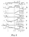
- regulator control circuit 29 turns on SCR S1 at a controllable instant t3 within the trace interval of a horizontal deflection period t1-t8 of the solid-line waveform FIGURES 2a-2g.
- the cathode voltage at terminal 14 equals the algebraic sum of the input voltage V i and the positive trace voltage v t (idealized as having a constant value V T ) of the flyback secondary winding voltage v s illustrated in FIGURE 2a.
- the voltage V L1 illustrated in FIGURE 2b, developed across regulator inductance L1, equals the difference in voltage between the voltage at terminal 14 and the voltage V0 developed at regulated B+ supply terminal 18.
Landscapes
- Engineering & Computer Science (AREA)
- Multimedia (AREA)
- Signal Processing (AREA)
- Power Engineering (AREA)
- Television Receiver Circuits (AREA)
- Dc-Dc Converters (AREA)
- Power Conversion In General (AREA)
- Details Of Television Scanning (AREA)
Abstract
Description
- This invention relates to a switching power supply for a television apparatus.
- In a television receiver, the amount of power delivered by the flyback transformer to an audio load circuit is limited by two factors. The first is audio induced modulation of scan size, and the second is temperature rise in the deflection semiconductor power components such as the horizontal output transistor. These limitations are especially severe when the television receiver uses an SCR regulator. Known but costly ways of overcoming these limitations include the use of a totally independent power supply when an audio output of more than approximately one watt per channel is required.
- A feature of the invention is a power supply that is capable of providing power to a load circuit from energy circulating within the existing switching power supply. A first switch is coupled to a source of DC input voltage and to an energy storage inductance for developing a source of DC supply voltage. Operation of the first switch generates a switched waveform voltage in the inductance. A first winding of a supply transformer is coupled to and energized by the source of DC supply voltage. A second switch is coupled to the first winding and is synchronously operated with the first switch to generate a switched waveform voltage in a second winding of the transformer that is in synchronism with the switched waveform voltage in the inductance. The second winding is coupled to the inductance and provides via the supply transformer a magnetic path for circulating energy to circulate between the source of DC supply voltage and the energy storage inductance. An auxiliary winding is magnetically coupled to the energy storage inductance and to a load circuit for transferring at least a portion of the circulating energy to the load circuit.
- In accordance with another feature of the invention, the energy supply requirement of a load circuit is shared between two switching power supply stages. A first switching stage is coupled to a source of DC input voltage and to a first transformer for generating first and second switched waveform voltages in first and second windings of the transformer. First and second filter stages are coupled to the first and second windings for developing respective first and second sources of DC supply voltage. A second switching stage is coupled to a first winding of a second transformer and to the first DC supply voltage for generating switched waveform voltages in the windings of the second transformer. A third filter stage is coupled to a second winding of the second transformer for developing a third source of DC supply voltage. The second and third sources of DC supply voltage are combined to develop a fourth source of DC supply voltage. A load circuit, such as the audio circuit, is energized by the fourth source from power jointly derived from the second and third sources of DC supply voltage.
- In the Drawing:
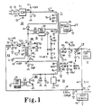
- FIGURE 1 illustrates a regulated switched power supply for a television apparatus, including an auxiliary power supply in accordance with the invention;
- FIGURES 2a-2g illustrate waveforms useful in explaining operation of the circuitry of FIGURE 1; and
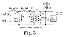
- FIGURE 3 illustrates the transformer equivalent circuit of the auxiliary power supply of FIGURE 1.
- In FIGURE 1, a switching
power supply stage 10 of a television apparatus includes a DCinput voltage source 130 comprising a source ofAC mains voltage 30 coupled betweeninput terminals wave bridge rectifier 31, for developing an unregulated DC input voltage Vi between an output terminal 34 and acurrent return terminal 35. Acapacitor 32 provides filtering of voltage Vi.Current return terminal 35 is designated as a hot ground, conductively nonisolated fromAC mains source 30 with respect to electrical shock hazard. - Unregulated voltage Vi is coupled to the anode of a controllable thyristor switching element SCR S1 of a switching stage SW1 via a winding W2 of a horizontal flyback supply transformer T1. One end of an energy storage inductance L1 is coupled to the cathode of SCR S1, the other end is coupled to a regulated
B+ supply terminal 18. A capacitor C0 provides filtering of a DC supply voltage supply V0 developed atterminal 18. A second switching element, diode D1 of switching stage SW1, has its anode coupled to the junction of SCR S1 and inductance L1 (terminal 14), and its cathode grounded tocurrent return terminal 35. - DC supply voltage V0 is coupled to and energizes the primary winding W1 of flyback transformer T1. A
horizontal deflection stage 20 is coupled to primary winding W1 and generates a switched waveform voltage retrace pulse vp (shown in Fig. 2a) at the dotted terminal of primary winding W1.Horizontal deflection circuit 20 includes a horizontal oscillator anddriver 21, a retrace capacitor 25, series coupled horizontal deflection winding 26 and S-shaping capacitor 27 and a trace switching arrangement SW2 comprising ahorizontal output transistor 23 and aparallel damper diode 24. A driver transformer 22 provides hot-cold electrical isolation withindeflection stage 20. - Flyback transformer T1 includes secondary windings W3, W4, W5 and W6 that are conductively isolated from
AC mains source 30. Winding W3 is a high voltage winding that energizes ahigh voltage circuit 28 for providing an ultor accelerating potential at a terminal U. A rectifier 42 is coupled to the undotted terminal of winding W4 and conducts during the trace interval of each deflection cycle to generate a DC supply voltage V3 at a terminal 49 that is filtered by acapacitor 43. Voltage V3 powers such load circuits of the television receiver asvertical deflection circuit 45. The dotted terminal of secondary winding W4 is coupled to aground reference potential 6 that is conductively isolated fromAC mains source 30 with respect to electrical shock hazard isolation. Arectifier 39 is coupled to the undotted terminal of winding W5 and conducts during the trace interval of each deflection cycle to generate a DC supply voltage V5 at aterminal 51 that is filtered by acapacitor 48. Voltage V5 provides a supply voltage to several of the television receiver integrated circuits, not shown in FIGURE 1. Other windings of flyback transformer T1, not illustrated in FIGURE 1, may provide other supply voltages and synchronizing signals to various circuits of the television receiver. - To regulate the B+ supply voltage V0 and the flyback transformer derived DC voltages, a
regulator control circuit 29 receives a feedback voltage Vf representative of variations in the supply voltages. Feedback voltage Vf is generated at the wiper arm of avariable resistor 16 that is part of a voltage divider,resistors terminal 51 and coldground reference potential 6. -
Regulator control circuit 29 generates gating pulses that are applied to SCR S1 via acoupling transformer 53 that also serves as a hot-cold isolation barrier. To synchronize the switching of SCR S1 and diode D1 with operation of trace switching arrangement SW2, a retrace pulse voltage is coupled toregulator control circuit 29 from a flyback transformer winding W6. - In operation,
regulator control circuit 29 turns on SCR S1 at a controllable instant t3 within the trace interval of a horizontal deflection period t1-t8 of the solid-line waveform FIGURES 2a-2g. With SCR S1 conducting, the cathode voltage atterminal 14 equals the algebraic sum of the input voltage Vi and the positive trace voltage vt (idealized as having a constant value VT) of the flyback secondary winding voltage vs illustrated in FIGURE 2a. The voltage VL1, illustrated in FIGURE 2b, developed across regulator inductance L1, equals the difference in voltage between the voltage atterminal 14 and the voltage V0 developed at regulatedB+ supply terminal 18. From time t3 to the end of the trace interval near time t4, voltage vL1 is positive and of relatively constant level VB. Voltage vL1 produces an upward ramp of current iL1 in inductance L1 that flows from output terminal 34 as an input current i1, illustrated in FIGURE 2c. Near the beginning of retrace, near time t4, input current i1 and thus current iL1 in inductance L1 has reached a peak value ILM1. - During the retrace interval, voltage vs in flyback winding W2 is a negative going pulse voltage vr of peak magnitude VP relative to AC zero. From the beginning of retrace, near time t4, until a later time t5 within retrace, voltage vL1 across inductance L1 follows in waveform the downwardly going retrace pulse voltage vr. During the interval t4-t5, input current i1 stops increasing and begins to decrease slightly as voltage VL1 reverses polarity under the influence of retrace pulse voltage vr.
- Near time t₅, voltage vL1 has decreased to a negative value -VA equal in magnitude to regulated B+ voltage V0 plus 1Vbe diode voltage drop. The voltage at
terminal 14, the junction of the cathodes of SCR S1 and diode D1, is just below ground potential, causing the diode to become conductive and take up the current flow in inductance L1. With diode D1 conducting near time t5, as illustrated by the diode current iD1 of FIGURE 2d, the cathode of SCR S1 is clamped to near ground potential. The anode voltage, however, continues to decrease under the influence of the negative retrace pulse voltage vr. SCR S1 quickly becomes nonconductive near time t5 due to the reverse biasing of the anode-to-cathode main current path in the SCR, as illustrated in FIGURE 2c by the input current i1 going to zero near time t5. - With diode D1 conducting, voltage vL1 is clamped to a negative voltage having a magnitude equal to the regulated B+ supply voltage level V0 plus the forward drop across diode D1, 1Vbe. The current iL1 in inductance L1 is a downwardly ramping current waveform illustrated by diode current iD1 of FIGURE 2d. Near time t7, the current in inductance L1 has decreased to zero and diode D1 becomes reverse biased as the current attempts to reverse direction. No current flows in inductance L1 after time t7 until
regulator control circuit 29 gates SCR S1 into conduction at a controllable instant during the trace interval of the next deflection cycle. - To regulate the B+ supply voltage and the output voltages of flyback transformer T1 against load and AC line variations,
regulator control circuit 29 varies the turn on instant of SCR S1 within the trace interval in accordance with the feedback voltage Vf. - The energy transfer and power flow within
main power supply 10 of FIGURE 1 will now be described. During the intervals t1-t3 and t5-t8, SCR S1 is nonconductive, and no input current i1 flows from supply terminal 34. During these intervals, there is no transfer of energy frominput voltage source 130. - From time t3, when SCR S1 is turned on, until the end of the trace interval, near time t4, an upramping current i1 flows from terminal 34, through flyback transformer winding W2, SCR S1 and inductance L1, to regulated
B+ supply terminal 18. During this interval, energy is being supplied byinput voltage source 130 and stored in inductance L1. Within the brief interval t4-t5 near the beginning of retrace, energy is being removed from inductance L1 by the decreasing current iL1. - During the early part of the trace interval, energy is flowing into horizontal B+ filter capacitor C0 from flyback transformer primary winding W1 when primary winding current ip is negative. During the interval t3-t4 when inductance current iL1 is reflected into primary winding current ip, energy is flowing out of B+ filter capacitor C0.
- During trace, between times t1-t4, regulated B+ voltage V0 is applied by trace switch SW2 across flyback transformer primary winding W1, with the undotted terminal of the winding being positive relative to the dotted terminal. Applied voltage V0 develops an upramping magnetizing current component to primary winding current ip, as indicated in Figure 2e by current ipa between times t1 and t3. After time t3, when SCR S1 is conductive, current i1 flowing in secondary winding W2 adds an additional component to the primary winding current due to the tight transformer coupling of windings W1 and W2. As illustrated in FIGURES 2c and 2e, during the interval t3-t5, when SCR S1 is conducting, current i1 is stepped down in accordance with the turns ratio Ns:Np of transformer T1. The portion ipb of primary winding current ip, therefore, includes both a magnetizing current component and a transformer coupled current component generated by input current i1. Omitted from illustration in FIGURE 2e is that component of the primary winding current that is generated by flyback transformer trace rectified supplies.
- During the early portion of the trace interval, when primary winding current ip is negative and the undotted terminal of primary winding W1 is positive, energy is flowing out of the primary winding into
B+ supply terminal 18 to be stored in filter capacitor C0. During the later portion of the trace interval, when both primary winding current ip and the voltage at the undotted terminal of the primary winding are positive, energy is flowing out ofB+ supply terminal 18 into primary winding W1. Part of this energy is stored in the flyback transformer in the form of increasing amplitude magnetizing current. - During the retrace interval, between times t4 and t8, the primary winding current is a generally resonant current ipc, illustrated in FIGURE 2e. The peak magnitude IM1 at the beginning of retrace is greater than the peak magnitude IM2 at the end of retrace, indicating a net transfer of energy via the flyback transformer to retrace driven load circuits, principally
high voltage circuit 28. - Because flyback transformer secondary winding W2 is coupled in series with SCR S1, the secondary winding also acts as a source of energy during the interval t3-t4 within trace when SCR S1 is conducting input current i1. As noted from FIGURES 2a and 2c, positive current i1 flows into the dotted terminal of secondary winding W2, which terminal is at a negative voltage during trace with respect to the undotted terminal. Energy, therefore, flows out of winding W2 towards inductance L1 and
B+ supply terminal 18. - The energy flowing out of secondary winding W2 is being supplied via the magnetics of flyback transformer T1 from the energy flowing into primary winding W1 from
B+ supply terminal 18. Thus, inpower supply stage 10, a circulating energy is created that circulates in a closed loop between primary winding W1 and secondary winding W2 via the magnetics of flyback transformer T1 and via the current path through SCR S1 and inductance L1. During the brief interval t4-t5 near the beginning of retrace, energy flows out of secondary winding W2 towardsterminal 18 when voltage vr of FIGURE 2a is positive, and energy flows into winding W2 from inductor L1 when voltage vr is negative. - In accordance with an aspect of the invention, the energy circulating between primary winding W1 and secondary winding W2 may be utilized by an
auxiliary power supply 40 to provide substantial power to a television receiver load circuit such asaudio circuit 46 of FIGURE 1. In carrying out this aspect of the invention, an auxiliary winding L2 is magnetically coupled to inductance L1 and wound around a common core to form an auxiliary supply transformer T2 that also serves as an electrical shock hazard isolation barrier. - With the winding polarities of windings L1 and L2 as shown in FIGURE 1, the undotted terminal of winding L2 is coupled to isolated
ground reference potential 6 and the dotted terminal is coupled to the anode of a rectifier D2. A filter capacitor C2 is coupled to the cathode of rectifier D2 at aauxiliary supply terminal 52.Supply terminal 52 is coupled to an audioB+ supply terminal 50 via a relatively small current limitingresistor 47. A filter capacitor 41 is coupled to audioB+ supply terminal 50. - In operation, when SCR S1 is conductive within each deflection cycle, during the interval t3-t5 of FIGURE 2, the dotted terminal of winding L1 is negative relative to the undotted terminal, producing a negative voltage vL2 of level -V′B at the dotted terminal of winding L2, as illustrated in FIGURE 2g. During the interval t4-t5 near the beginning of retrace, voltage vL2, being the transformed voltage of voltage vL1, follows in waveshape an opposite polarity version of voltage vr of FIGURE 2a.
- After time t5, retrace pulse voltage vr cuts off conduction in SCR S1 and diode D1 takes over current flow in winding L1. The regulated B+ supply voltage V0 is impressed by diode D1 across winding L1 and by transformer action develops a positive voltage vL2 of amplitude V′A after time t5, as illustrated in FIGURE 2g. Diode D2 becomes forward biased and charges filter capacitor C2 to devlop an auxiliary DC supply voltage V2 at terminal 52 equal to voltage level V′A less 1Vbe.
- Operation of
auxiliary power supply 40 will now be explained with the aid of its electrical equivalent circuit illustrated in FIGURE 3. In FIGURE 3, an ideal transformer T2′ includes a primary winding WL1, corresponding to winding L1 of FIGURE 1, and having the same number of turns N1. Transformer T2′ includes a secondary winding WL2, corresponding to winding L2, and having the same number of turns N2. Inductance lp corresponds to the primary leakage inductance of transformer T2 of FIGURE 1, inductance ls corresponds to the secondary leakage inductance of transformer T2 reflected back to the primary, and inductance Lm corresponds to the shunt or magnetizing inductance of transformer T2. Diode D2 of FIGURE 1 has been transformed to the primary side in FIGURE 3 and is in series with secondary leakage inductance ls. Diode D1 in FIGURE 1 is shown in FIGURE 3 as being in series with primary leakage inductance lp. Generalized impedance ZL corresponds to the audio load coupled toterminal 52 of FIGURE 1. - Current iL2 of FIGURE 1 is shown in FIGURE 3 as flowing in ideal transformer secondary winding WL2. This current is transformed into a primary winding current i′L1 flowing in ideal transformer primary winding WL1 and in secondary leakage inductance ls. The diode current iD1 of FIGURE 1 is shown in FIGURE 3 as flowing in primary leakage inductance lp. A magnetizing current im may be defined in the transformer equivalent circuit of FIGURE 3 as flowing in magnetizing inductance Lm and equals the algebraic sum of diode current iD1 and the transformed version i′L1 of secondary winding current iL2.
- The transformer equivalent circuit of FIGURE 3 comes into existence at time t5 of FIGURE 2, when SCR S1 is cutoff by retrace pulse voltage vr and diode D1 takes over current conduction. Thus, at time t5 of FIGURE 2d, current iD1 of FIGURE 3 is at a maximum value IMa equal in magnitude to the current in SCR S1 at its cutoff instant. Secondary winding current iL2 and its reflected current i′L1 are both zero prior to time t5 due to the blocked state of diode D2.
- At time t5, when diode D1 becomes conductive, voltage V0 developed across capacitor C0 is applied to winding WL1 of FIGURE 3 via the T-network impedance (lp,Lm,ls) to develop voltage Vl′ across winding WL1, where the dotted terminal of the winding is made positive. With diode D1 conducting at time t5, voltage V0 developed across capacitor C0 is impressed across the series coupled inductances lp and Lm.
- Because magnetizing inductance Lm is much larger than primary leakage inductance lp, voltage Vm developed across the magnetizing inductance is nearly equal to voltage V0. Because of the loading effects by audio load ZL, auxiliary supply voltage V2 and thus the transformed auxiliary supply voltage V1′ is even lower in magnitude than voltage Vm. Transformed current i′L1 begins to flow at time t5 through forward biased diode D2 and through transformed secondary leakage inductance ls and magnetizing inductance Lm. As illustrated in FIGURE 2f, the transformed current i′L1 begins to ramp up at time t5 with a slope that is determined in accordance with the difference in voltage between voltage Vm and voltage V1′ and in accordance with the value of transformed secondary leakage inductance ls. As current i′L1 of FIGURE 2f ramps up, current iD1 of FIGURE 2d ramps down, with the sum of the two currents being equal to magnetizing current im.
- At time t7, current in diode D1 in FIGURE 3 has ramped down to zero and the diode becomes reverse biased, removing voltage V0 and primary linkage inductance lp from the remainder of the circuit. After time t7, the transformed auxiliary supply voltage V1′ is impressed across the series arrangement of magnetizing inductance Lm and transformed secondary leakage inductance ls. Current i′L1 in winding WL1 begins ramping down to zero from its peak magnitude, reaching zero at time t9 of FIGURE 2f, at which time diode D2 becomes blocked. During the interval t5-t9 when transformed current i′L1 flows, capacitor C2 is charged by secondary winding current iL2 to replenish charge lost to audio load ZL.
- In accordance with a feature of the invention,
auxiliary power supply 40 inherently provides load regulation of auxiliary supply voltage V2 when the power supply is used in conjunction with amain power supply 10 that regulates horizontal B+ supply voltage V0. - Consider an example of increased audio loading from e.g. 3 watts to e.g. 23 watts. The dashed-line waveforms in FIGURE 2 apply to such a situation. To provide the additional audio load power from
input supply 130 while maintaining regulated B+ voltage V0 unchanged,regulator control circuit 29 turns on SCR S1 at the earlier instant t2 of FIGURE 2c. Input current i1 ramps up for a longer interval within trace, reaching a higher peak magnitude iLm2, indicating more stored energy in inductor L1 at time t5 when SCR S1 is cutoff and diode D1 takes up the current flow. As illustrated in the dashed-line waveform of current iD1 in FIGURE 2d, the peak diode current iMb at time t5 is increased over the solid-line waveform, light loading situation. - At time t5, when the transformer equivalent circuit of FIGURE 3 is created, the transformed auxiliary supply voltage V1′ tends to be of decreased magnitude due to the increased audio loading. In contrast, B+ supply voltage V0 and thus magnetizing voltage Vm tend to remain stabilized by operation of
main power supply 10. The voltage impressed across transformed secondary leakage inductance ls, being the difference in voltage between magnetizing voltage Vm and transformed auxiliary supply voltage V1′, is a greater impressed voltage under heavy audio loading than under light audio loading. Because of the greater impressed voltage, current i′L1 and corresponding current iL2 ramp up at a much greater rate under heavy loading than under light loading, as noted in FIGURE 2f by comparing the dashed-line waveform with the solid-line waveform. - Since magnetizing current im equals the sum of currents iD1 and i′L1, the rapid upramp of current i′L1 results in a rapid downramp of current iD1 from its peak value iMb, as illustrated by the dashed-line waveform in FIGURE 2d. This current, under heavy loading conditions, reaches zero at a much earlier time, time t6.
- At time t6, diode D1 becomes blocked and currents i′L1 and iL2 begin their downramping from time t6 until time t10, at which time diode D2 becomes blocked. One notes from FIGURE 2f, that under heavy loading, current iL2 ramps up to a much greater peak magnitude IMs2 and after time t6 ramps down at a rate mainly determined by the values of transformed auxiliary supply voltage V1′ and the inductance of magnetizing inductance Lm. The inductance of transformed secondary leakage inductance ls, being much smaller than magnetizing inductance Lm, has very little influence on the rate that currents i′L1 and iL2 ramp down.
- The amount of energy transferred to auxiliary supply capacitor C2 to replenish losses incurred in audio load ZL is represented by the area under the curve iL2 of FIGURE 2f. The area under the dashed-line waveform of current iL2, representing a heavy audio loading situation, is greater than the area under the solid-line waveform, representing a light loading condition.
- Similarly, the area under the waveform of current iD1 of FIGURE 2d represents energy returned to B+ filter capacitor C0. This energy is obtained from the energy stored in inductor L1 at time t5 when SCR S1 becomes cutoff. Under heavy loading, the amount of energy supplied to B+ filter capacitor C0 is smaller than the amount of energy supplied under light loading.
- The energy stored in inductor L1 at time t5, is completely removed from the inductor by the time diode D2 in
auxiliary power supply 40 becomes blocked. The energy removed from inductor L1 goes to two places. Part of the energy goes to B+ filter capacitor C0 when the capacitor is charged by diode current iD1, and the remaining part goes to auxiliary supply capacitor C2 when that capacitor is charged by current iL2. - Comparing the dashed-line waveforms of FIGURES 2d and 2f with the solid-line waveforms, one notes that under heavy loading, more of the energy stored in inductance L1 at time t5 goes to auxiliary supply capacitor C2 to replenish the heavy load losses than is supplied to B+ filter capacitor C0. Under light loading, the reverse is true; more of the stored energy is supplied to B+ filter capacitor C0 and less goes to auxiliary supply capacitor C2.
- The design parameters of transformer T2 in
auxiliary power supply 40 are such as to automatically maintain auxiliary supply voltage V2 well regulated over a wide range of audio loading from minimal audio loading of e.g. 3 watts to heavy audio loading of e.g. 23 watts. Inherent in the transformer equivalent circuit ofauxiliary power supply 40 in FIGURE 3 is the large increase in auxiliary supply current iL2 in response to a very small load induced decrease in auxiliary supply voltage V2. For example, under light audio loading, auxiliary supply voltage V2 may equal a value of 25 volts; whereas, under heavy audio loading, voltage V2 may decrease by only one or two volts to a level of 24 or 23 volts. - The amount of audio loading may be increased until a point is reached where practically all of the energy stored in inductor L1 at time t5 goes to auxiliary supply capacitor C2 and none is supplied to B+ filter capacitor C0. When this point is reached, any further increase in audio loading does not result in more energy being transferred to capacitor C2. Under these circumstances, auxiliary supply voltage V2 decreases rapidly as more energy is being removed from capacitor C2 than is being supplied to the capacitor.
- In accordance with a feature of the invention, the maximum amount of energy that may be supplied by
auxiliary power supply 40 is enhanced by the presence of flyback transformer secondary winding W2 being in-circuit with SCR S1. When SCR S1 is conducting, input current i₁ flows in inductor L2. This current must of necessity also flow in winding W2. - The upramping input current i1 stores energy in inductor L1 for subsequent transfer out after time t5. A source of this energy is
input voltage source 130; another source is the circulating energy that circulates from regulatedB+ supply terminal 18 to primary winding W1 and then into secondary winding W2 via the magnetics of flyback transformer T1. This circulating energy is then routed to inductor L1. - The amount of energy stored in inductor L1 is greater than the amount of energy being supplied to it solely by
input source 130. Advantageously, the greater stored energy in inductor L1, derived from the circulating energy, is able to support a greater maximum audio loading. - The amount of energy stored in inductor L1 at time t5 is least under conditions of low AC mains supply voltage and light beam current loading on flyback transformer T1. In such a situation, heavy audio loading may tend to reach or exceed the design limit of
auxiliary power supply 40, tending to cause auxiliary supply voltage V2 and thus audio B+ supply voltage V4 at terminal 50 to decrease more than may be desirable. - In accordance with another feature of the invention, power for dynamically varying
audio load circuit 46 of FIGURE 1 may be derived jointly fromauxiliary power supply 40 and switchingpower supply stage 10. To accomplish this result, a flyback transformer secondary supply voltage such as vertical B+ supply voltage V3 is coupled to audioB+ supply terminal 50 via a current limitingresistor 44.Resistor 44 is coupled between vertical B+ supply terminal 49 and audioB+ supply terminal 50. - As the need arises, current may be supplied to audio
B+ supply terminal 50 either fromauxiliary supply terminal 52 via the small valued current limitingresistor 47 or may be supplied from vertical B+ supply terminal 49 via the small valued current limitingresistor 44. Current limitingresistor 47 is made significantly smaller than current limitingresistor 44, e.g. 5 to 10 times smaller. Vertical B+ supply voltage V3 is designed to have a nominal value close to that of audio B+ supply voltage V4. Choosing the vertical B+ supply voltage as the supplemental voltage is advantageous from the point of view of being a high power supply source of approximately the same voltage level as the audio B+ supply voltage. - Under all but the most extreme loading by
audio load circuit 46, load current and power flows mainly fromauxiliary supply terminal 52 via the smaller valuedresistor 47. At the maximum or limit load condition, when voltage V2 atauxiliary supply terminal 52 tends to begin decreasing significantly, vertical B+ supply terminal 49 provides a substantial amount of the load current viaresistor 44. Thus, even under extreme audio loading conditions, audio B+ supply voltage V4 may be maintained relatively stable by the additional supply voltage source available viaresistor 44. - The values for voltages V2, V3 and V4 illustrated in FIGURE 1 are for heavy audio loading of 23 watts. Approximately two-thirds of the load current and power flows from auxiliary supply winding L2 via
terminal 52, and one-third flows from flyback transformer secondary winding W4 via terminal 49. The relative contributions of power toaudio load circuit 46 fromsupply terminals 52 and 49 may be changed by adjusting the values ofresistors - For light audio loading of around three watts, the approximate voltage values are as follows: voltage V2=25.5V, voltage V3=25V, and voltage V4=25.4V. Audio B+ supply voltage V4 is slightly greater than vertical B+ supply voltage V3, indicating that a slight amount of current is flowing from
auxiliary supply terminal 52 to vertical B+ supply terminal 49 via audioB+ supply terminal 50. In this situation all the audio load power is being supplied byauxiliary power supply 40. By changing the parameters ofauxiliary power supply 40, such as the turns ratio of transformer T2 or the values ofresistors auxiliary supply terminal 52. - The increased loading on vertical B+ supply terminal 49 due to the heavy audio loading tends to increase the AC ripple across vertical
B+ filter capacitor 43. The vertical amplifier negative feedback circuitry withinvertical deflection 45 may be unable to respond fast enough to the audio load induced ripple to avoid undesirable modulation of the vertical deflection amplitude and of the raster height. - In accordance with a further aspect of the invention, the ripple voltage developed across vertical
B+ filter capacitor 43 is AC coupled toregulator control circuit 29 via aresistor 13 and acapacitor 8 that are coupled in series between vertical B+ supply terminal 49 and the wiper arm ofresistor 16. The AC ripple acrosscapacitor 43 contributes a component to feedback voltage Vf that modulates the turn-on time of SCR S1 in such a manner as to modify regulated B+ voltage V0 in a direction to cancel out the audio induced ripple. The horizontal rate switching of SCR S1 is sufficiently rapid to enablepower supply stage 10 to follow and compensate for the audio induced ripple in vertical B+ supply voltage V3.
Claims (10)
a source of DC input voltage;
an energy storage inductance; characterized by
a first switching arrangement (SW1) coupled to said DC input voltage (Vi) and to said inductance (L1) for developing a first source (VO) of DC supply voltage, operation of said first switching arrangement (SW1) generating a first switched waveform voltage (VL1) in said inductance (L1);
a supply transformer (T1) having a first winding (W1) coupled to and energized by said first source (VO) of DC supply voltage;
a second switching arrangement (SW2) coupled to said first winding (W1) and synchronously operated with said first switching arrangement (SW1) to generate a second switched waveform voltage in said first winding (W1) that is synchronized (by W6) with the first switched waveform voltage (VL1);
a second winding (W2) of said supply transformer (T1) coupled to said inductance (L1) for providing via said supply transformer (T1) a magnetic path for circulating energy to circulate between said first source of DC supply voltage (VO) and said energy storage inductance (L1);
a load circuit (46); and
an auxiliary winding (L2) magnetically coupled to said energy storage inductance (L1) and coupled to said load circuit (46) for transferring at least a portion of said circulating energy to said load circuit (46).
a source of DC input voltage;
a source of a deflection rate voltage;
an energy storage inductance;
a controllable switching element having a main current path coupled to said source of DC input voltage and to said inductance; characterized by
a deflection rate pulse transformer (T1) coupled to said inductance (L1) and to a first load circuit (20);
a control circuit (29) coupled to said controllable switching element (S1) for switching said main current path to the conductive state each deflection cycle at a controllable instant within a first polarity interval (trace interval) of said deflection rate voltage to store in said inductance (L1) a controllable amount of energy from both sources;
a second switching element (D1) coupled to said main current path, to said source (W2) of a deflection rate voltage (VS), and to said inductance (L1) for switching said main current path to the nonconductive state during an opposing polarity interval (retrace interval) of said deflection rate voltage (VS), the energy stored in said inductance (L1) being depleted during said opposing polarity interval to replenish, via said pulse transformer (T1), losses sustained in said first load circuit (20);
a supply winding (L2) magnetically coupled to said energy storage inductance (L1); and
a rectifier circuit (D2,C2) coupled to said supply winding (L2) and to a second load circuit (46) and poled for conduction during said opposing polarity interval of said deflection rate voltage (VS) for further depleting the energy stored in said inductance (L1) to replenish, via said supply winding (L2), losses sustained in said second load circuit (46).
a source of DC input voltage;
a first transformer having first and second windings; characterized by
a first switching stage (SW1) coupled to said first transformer (T2) for generating first and second switched waveform voltages in said first (L1) and second (L2) windings;
first (CO) and second (C2) filter stages coupled to said first (L1) and second (L2) windings respectively for developing respective first (VO) and second (V2) sources of DC supply voltages;
a second transformer (T1) having first (W1) and second (W4) windings;
a second switching stage (SW2) coupled to the first winding (W1) of said second transformer (T1) and to said first DC supply voltage (VO) for energizing said second transformer (T1) to generate switched waveform voltages in the first (W1) and second (W4) windings of said second transformer (T1);
a third filter stage (43) coupled to said second winding (W4) of said second transformer (T1) for developing a third source (V3) of DC supply voltage;
means (44,47) for combining said second (V2) and third (V3) sources of DC supply voltage to develop a fourth source (V4) of DC supply voltage; and
a dynamically varying load circuit (46) energized by said fourth source (V4) of DC supply voltage and being supplied by power derived jointly from said second (V2) and third (V3) sources of DC supply voltage, such that under heavy loading both said second (V2) and (V3) third sources of DC supply voltage supply substantial amounts of power to said load circuit (46).
Applications Claiming Priority (2)
| Application Number | Priority Date | Filing Date | Title |
|---|---|---|---|
| US07/194,643 US4829216A (en) | 1988-05-16 | 1988-05-16 | SCR regulator for a television apparatus |
| US194643 | 1988-05-16 |
Publications (2)
| Publication Number | Publication Date |
|---|---|
| EP0342503A2 true EP0342503A2 (en) | 1989-11-23 |
| EP0342503A3 EP0342503A3 (en) | 1991-09-25 |
Family
ID=22718367
Family Applications (1)
| Application Number | Title | Priority Date | Filing Date |
|---|---|---|---|
| EP19890108399 Ceased EP0342503A3 (en) | 1988-05-16 | 1989-05-10 | Scr regulator for a television apparatus |
Country Status (7)
| Country | Link |
|---|---|
| US (1) | US4829216A (en) |
| EP (1) | EP0342503A3 (en) |
| JP (1) | JP2781919B2 (en) |
| KR (1) | KR0137273B1 (en) |
| CN (1) | CN1018228B (en) |
| CA (1) | CA1300743C (en) |
| FI (1) | FI93412C (en) |
Families Citing this family (8)
| Publication number | Priority date | Publication date | Assignee | Title |
|---|---|---|---|---|
| US5283654A (en) * | 1989-07-12 | 1994-02-01 | Samsung Electronics Co. Ltd. | TV-radio converter using a same power supply |
| MY108974A (en) * | 1992-05-29 | 1996-11-30 | Thomson Consumer Electronics Inc | Tracking run/standby power supplies |
| US5377090A (en) * | 1993-01-19 | 1994-12-27 | Martin Marietta Corporation | Pulsed power converter with multiple output voltages |
| US5422589A (en) * | 1993-11-05 | 1995-06-06 | Acer Peripherals, Inc. | Circuit for synchronizing an operating clock of a switching power supply system |
| US7269034B2 (en) | 1997-01-24 | 2007-09-11 | Synqor, Inc. | High efficiency power converter |
| AU722043B2 (en) | 1997-01-24 | 2000-07-20 | Synqor, Inc. | High efficiency power converter |
| US10199950B1 (en) | 2013-07-02 | 2019-02-05 | Vlt, Inc. | Power distribution architecture with series-connected bus converter |
| KR102521718B1 (en) * | 2016-11-01 | 2023-04-14 | 삼성전자주식회사 | Supply modulator including switched-mode power supplier and transmitting device including the same |
Family Cites Families (14)
| Publication number | Priority date | Publication date | Assignee | Title |
|---|---|---|---|---|
| GB1309661A (en) * | 1969-04-25 | 1973-03-14 | Philips Electronic Associated | Circuit arrangements for television picture display apparatus |
| BE748171A (en) * | 1969-04-25 | 1970-09-28 | Philips Nv | CIRCUIT EQUIPPING WITH AN IMAGE REPRODUCTION DEVICE |
| US3970780A (en) * | 1972-10-04 | 1976-07-20 | Sharp Kabushiki Kaisha | Constant-voltage power supply |
| FR2261670A1 (en) * | 1974-02-15 | 1975-09-12 | Thomson Brandt | Television receiver power supply unit - avoids three position switch can operate from direct or alternating curent mains |
| GB1551013A (en) * | 1975-11-07 | 1979-08-22 | Rca Corp | Power supply arrangement with minimum interaction between plural loads |
| DE2749847C2 (en) * | 1977-11-08 | 1988-01-21 | Licentia Patent-Verwaltungs-Gmbh, 6000 Frankfurt | Switching power supply for a radio receiver, in particular a television receiver |
| US4190791A (en) * | 1978-11-02 | 1980-02-26 | Rca Corporation | Switching regulator for television deflection circuit with improved ultor voltage regulation |
| US4163926A (en) * | 1978-09-07 | 1979-08-07 | Rca Corporation | Switching regulator for a television apparatus |
| FI60626C (en) * | 1979-08-14 | 1982-02-10 | Salora Oy | STROEMKAELLA |
| US4484113A (en) * | 1981-02-16 | 1984-11-20 | Rca Corporation | Regulated deflection circuit |
| US4524411A (en) * | 1982-09-29 | 1985-06-18 | Rca Corporation | Regulated power supply circuit |
| US4466051A (en) * | 1982-10-25 | 1984-08-14 | Rca Corporation | Regulated power supply incorporating a power transformer having a tightly coupled supplemental power transfer winding |
| NL8301263A (en) * | 1983-04-11 | 1984-11-01 | Philips Nv | POWER SUPPLY CIRCUIT. |
| US4692852A (en) * | 1986-06-25 | 1987-09-08 | Rca Corporation | Switching power supply with raster width stabilization |
-
1988
- 1988-05-16 US US07/194,643 patent/US4829216A/en not_active Expired - Fee Related
-
1989
- 1989-04-27 CA CA000598069A patent/CA1300743C/en not_active Expired - Lifetime
- 1989-05-09 FI FI892227A patent/FI93412C/en not_active IP Right Cessation
- 1989-05-10 EP EP19890108399 patent/EP0342503A3/en not_active Ceased
- 1989-05-13 CN CN89103309A patent/CN1018228B/en not_active Expired
- 1989-05-15 JP JP1122676A patent/JP2781919B2/en not_active Expired - Lifetime
- 1989-05-15 KR KR1019890006457A patent/KR0137273B1/en not_active Expired - Fee Related
Also Published As
| Publication number | Publication date |
|---|---|
| CA1300743C (en) | 1992-05-12 |
| FI93412C (en) | 1995-03-27 |
| JPH0271686A (en) | 1990-03-12 |
| JP2781919B2 (en) | 1998-07-30 |
| KR0137273B1 (en) | 1998-04-28 |
| CN1018228B (en) | 1992-09-09 |
| FI892227A7 (en) | 1989-11-17 |
| FI93412B (en) | 1994-12-15 |
| US4829216A (en) | 1989-05-09 |
| EP0342503A3 (en) | 1991-09-25 |
| KR900019361A (en) | 1990-12-24 |
| FI892227A0 (en) | 1989-05-09 |
| CN1037818A (en) | 1989-12-06 |
Similar Documents
| Publication | Publication Date | Title |
|---|---|---|
| US5517397A (en) | Flyback power converter with spike compensator circuit | |
| CA1160354A (en) | Power supply and deflection circuit with raster size compensation | |
| GB2064251A (en) | Deflection and power supply circuit with reduced start-up drive | |
| KR920005869B1 (en) | East-West Pincushion Correction Horizontal Deflection Circuit | |
| US4829216A (en) | SCR regulator for a television apparatus | |
| EP0490265B1 (en) | Transformer coupled voltage clamp for pincushion correction circuit | |
| US4321514A (en) | Commutated SCR regulator for a horizontal deflection circuit | |
| PL133148B1 (en) | Deflecting system with correction of distortion of tv image matrix | |
| US4484113A (en) | Regulated deflection circuit | |
| US4604556A (en) | Television receiver load compensation circuit | |
| JP2781917B2 (en) | Power supply for television receiver | |
| US5266871A (en) | High voltage stabilization circuit for video display apparatus | |
| US4572993A (en) | Television deflection circuit with raster width stabilization | |
| GB2262822A (en) | A synchronised switch-mode power supply | |
| JPS62204666A (en) | deflection device | |
| GB2119209A (en) | Variable horizontal deflection circuit capable of providing eastwest pincushion correction | |
| US4118655A (en) | Line sawtooth deflection current generator | |
| EP0521659B1 (en) | High voltage stabilization circuit for video display apparatus | |
| KR920004104B1 (en) | Television receiver load compensation circuit | |
| EP1185085A1 (en) | A deflection circuit with a feedback controlled capacitive transformation | |
| EP0527471B1 (en) | High voltage generator | |
| US5012164A (en) | Horizontal deflection and EHT generator circuit | |
| JPH0439266B2 (en) | ||
| EP0204369A2 (en) | Deflection circuit | |
| JPH07274030A (en) | Horizontal deflection high voltage generation circuit |
Legal Events
| Date | Code | Title | Description |
|---|---|---|---|
| PUAI | Public reference made under article 153(3) epc to a published international application that has entered the european phase |
Free format text: ORIGINAL CODE: 0009012 |
|
| AK | Designated contracting states |
Kind code of ref document: A2 Designated state(s): AT DE ES FR GB IT SE |
|
| PUAL | Search report despatched |
Free format text: ORIGINAL CODE: 0009013 |
|
| AK | Designated contracting states |
Kind code of ref document: A3 Designated state(s): AT DE ES FR GB IT SE |
|
| 17P | Request for examination filed |
Effective date: 19920317 |
|
| 17Q | First examination report despatched |
Effective date: 19931228 |
|
| STAA | Information on the status of an ep patent application or granted ep patent |
Free format text: STATUS: THE APPLICATION HAS BEEN REFUSED |
|
| 18R | Application refused |
Effective date: 19950520 |