EP0336725B1 - Switching power supply - Google Patents
Switching power supply Download PDFInfo
- Publication number
- EP0336725B1 EP0336725B1 EP89303338A EP89303338A EP0336725B1 EP 0336725 B1 EP0336725 B1 EP 0336725B1 EP 89303338 A EP89303338 A EP 89303338A EP 89303338 A EP89303338 A EP 89303338A EP 0336725 B1 EP0336725 B1 EP 0336725B1
- Authority
- EP
- European Patent Office
- Prior art keywords
- voltage
- current
- output
- winding
- switching element
- Prior art date
- Legal status (The legal status is an assumption and is not a legal conclusion. Google has not performed a legal analysis and makes no representation as to the accuracy of the status listed.)
- Expired - Lifetime
Links
Images


Classifications
-
- H—ELECTRICITY
- H02—GENERATION; CONVERSION OR DISTRIBUTION OF ELECTRIC POWER
- H02M—APPARATUS FOR CONVERSION BETWEEN AC AND AC, BETWEEN AC AND DC, OR BETWEEN DC AND DC, AND FOR USE WITH MAINS OR SIMILAR POWER SUPPLY SYSTEMS; CONVERSION OF DC OR AC INPUT POWER INTO SURGE OUTPUT POWER; CONTROL OR REGULATION THEREOF
- H02M3/00—Conversion of dc power input into dc power output
- H02M3/22—Conversion of dc power input into dc power output with intermediate conversion into ac
- H02M3/24—Conversion of dc power input into dc power output with intermediate conversion into ac by static converters
- H02M3/28—Conversion of dc power input into dc power output with intermediate conversion into ac by static converters using discharge tubes with control electrode or semiconductor devices with control electrode to produce the intermediate ac
- H02M3/325—Conversion of dc power input into dc power output with intermediate conversion into ac by static converters using discharge tubes with control electrode or semiconductor devices with control electrode to produce the intermediate ac using devices of a triode or a transistor type requiring continuous application of a control signal
- H02M3/335—Conversion of dc power input into dc power output with intermediate conversion into ac by static converters using discharge tubes with control electrode or semiconductor devices with control electrode to produce the intermediate ac using devices of a triode or a transistor type requiring continuous application of a control signal using semiconductor devices only
- H02M3/33569—Conversion of dc power input into dc power output with intermediate conversion into ac by static converters using discharge tubes with control electrode or semiconductor devices with control electrode to produce the intermediate ac using devices of a triode or a transistor type requiring continuous application of a control signal using semiconductor devices only having several active switching elements
- H02M3/33576—Conversion of dc power input into dc power output with intermediate conversion into ac by static converters using discharge tubes with control electrode or semiconductor devices with control electrode to produce the intermediate ac using devices of a triode or a transistor type requiring continuous application of a control signal using semiconductor devices only having several active switching elements having at least one active switching element at the secondary side of an isolation transformer
- H02M3/33584—Bidirectional converters
Definitions
- This invention relates to a switching power supply for supplying DC stabilized voltages to industrial and consumer equipments.
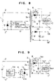
- the conventional switching power supply has such an arrangement as shown in Fig. 22.
- a DC power supply 1 which is obtained by rectifying and smoothing an AC voltage or formed of a battery.
- This DC power supply is connected between input terminals 2, 2' so as to supply a positive voltage to the input terminal 2 and a negative voltage to the input terminal 2'.
- Shown at 3 is a transformer which has one end of a primary winding 3a connected to the input terminal 2, the other end thereof connected through a switching element 4 to the input terminal 2', one end of a secondary winding 3c connected to an output terminal 11', the other end thereof connected through a diode 7 to an output terminal 11, one end of a bias winding 3b connected to the input terminal 2', and the other end thereof connected to a synchronizing oscillation control circuit 13.
- the switching element 4 is turned on and off when supplied at its control terminal with an on-off signal from the synchronizing oscillation control circuit 13, thereby interrupting the input voltage to the primary winding 3a.
- the synchronizing oscillation control circuit 13 controls to change the on-period of the element 4 by the output signal from insulating transmission means 14 such as photocouplers and keeps the off-state until the voltage across the bias winding 3b is reversed in its polarity.
- the rectifying diode 7 has its anode connected to one end of the secondary winding 3c and its cathode connected to the output terminal 11. Shown at 9 is a smoothing capacitor, which is connected between the output terminals 11, 11'.
- the rectifying diode 7 rectifies the voltage induced in the secondary winding 3c connected between the output terminals 11, 11' and the smoothing capacitor 9 acts to smooth the rectified voltage and to supply it to the output terminals as the output voltage.
- Shown at 15 is an error amplifier which compares a reference voltage 16 and the output voltage between the output terminals 11, 11', amplifies the compared signal and supplies it to the insulating transmission means 14.
- the insulating transmission means 14 acts to insulate between the primary and secondary windings and to transmit the signal from the error amplifier 15 to the synchronizing oscillation control circuit 13. The operation of this conventional example will be described below.
- a similar voltage is also generated across the bias winding 3b of the transformer 3, and tends to change to the polarity opposite to that of the flyback voltage.
- the change of polarity is transmitted to the synchronizing oscillation control circuit 13, again turning on the switching element 4. Repetition of these operations provides a continuous output voltage from the terminals 11, 11'.
- Fig. 23 Shown in Fig. 23 at (a) is a voltage waveform V Ds across the switching element 4, at (b) is a primary current I D which flows in the primary winding 3a, at (c) is a drive pulse waveform V G from the synchronizing oscillation control circuit 13 and at (d) is a secondary current waveform 1 0 which flows in the secondary winding 3c.
- the solid lines indicate a so-called over-load time in which a large amount of output current l OUT flows out of the output terminals 11, 11', and the broken lines indicate a so-called light-load time in which a small amount of output current l OUT flows out of the terminals.
- the current l OUT is expressed by the output voltage Vou T by the switching frequency f by where N s is the number of turns of the secondary winding 3c, Np is the number of turns of the primary winding 3a, L s is the inductance of the secondary winding 3c, V IN is the input voltage supplied from the DC power supply 1, TON is the on-period of the switching element 4, TOFF is the off-period of the switching element 4 and T is the oscillation period.
- the output voltage V OUT is compared with the reference voltage 16 in the error amplifier 15 and the compared result is supplied through the insulation transmission means 14 to the synchronizing oscillation control circuit 13, thereby controlling the on-period of the switching element 4. Therefore, the output voltage is always controlled to be constant with the on-period changed even though the output current l OUT and the input voltage V IN are changed.
- Fig. 23 shows such situations. However, since the change of the on-period results in the change of the off-period, the oscillation frequency f is also changed as is obvious from the figure.
- the synchronizing oscillation control circuit 13 has the function of limiting the maximum on-period or the primary current.
- the voltage and current waveforms to be supplied when the switching element 4 is turned on and off are simultaneously changed while crossing each other due to the gradients depending on the response speed of the switching element 4, thus causing a large switching loss.
- the switching loss is decreased by increasing the response speed of the switching element 4, the voltage and current waveforms become steeper, leading to increase of the switching noise and the voltage and current spikes which are supplied to the switching element 4.
- Fig. 24 shows an arrangement of a conventional resonant-type switching power supply.
- like elements corresponding to those in Fig. 22 are identified by the same reference numerals and will not be described.
- These inductance 45 and the capacitance 41 constitute an LC resonant circuit.
- Shown at 5 is a diode which is connected across the switching element 4.
- This diode has its anode connected to the input terminal 2' and its cathode connected one end of the primary winding 3a, so that when the energy stored in the inductance 45 is released bach to the DC power supply 1, a current can be flowed in the winding even under the off-state of the switching element 4.
- Shown at 42 is a synchronizing oscillation control circuit which generates an on-off control signal to the switching element 4 and detects the current in the diode 5 so that the on-period of the switching element 4 is changed and the off-period is maintained until a current flows in the diode 5.
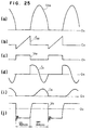
- Fig. 25 shows a operating waveforms at each portions.
- the voltage waveforms VDS across the switching element 4 at (b) a current waveform I' os which flows in the switching element 4 and in the diode 5, at (c) a drive pulse waveform V G1 from the synchronizing oscillation control circuit 42, at (d) a current waveform I' c flowing in the capacitor 41, at (i) a secondary current waveform 1 0 flowing in the secondary winding 3c, and (j) an induced voltage waveform V o across the secondary winding 3c.
- the values of the inductances 45 and capacitor 41 and the on-period are set so that the amplitude becomes much larger than the sum of the input voltage and the flyback voltage, causing the voltage across the capacitor 41 to be negative.
- This negative-voltage period causes the voltage across the capacitor 41 to be zero and a current is flowed in the inductance 45 through the diode 5.
- the switching element 4 is turned on by the synchronizing oscillation control circuit 42, but no discharge current is flowed from the capacitor 41 to the switching element 4, thus the so-called zero-cross switching being caused in which the switching element is in the on-state with zero voltage applied there across. This operation is repeated to supply the output voltage to the output terminals 11, 11'.
- the voltage waveform (current waveform or both voltage and current waveforms depending on the system) applied when the switching element 4 is turned on and turned off gently changes with a sine-wave gradient irrespective of the response speed of the switching element 4.
- the switching loss is small and since the voltage waveform is a sine wave, the switching noise is very little.
- the switching element 4 when the switching element 4 is turned on, the above zero-cross switching must be made, otherwise the capacitor 41 would be shorted through the switching element 4, thus breaking the switching element 4, or the switching loss would be suddenly increased or the switching noise would be increased.
- the voltage (or current)waveform applied to the switching element 4 is rectangular, but in the resonant-type it is a sine wave, so that the peak value of the applied waveform increases. This follows that the switching element 4 is required to have a large capacity and that a large resonant current is flowed through the inductance 45, capacitor 41 and primary winding 3C to the DC power supply 1.
- Fig. 26 shows another conventional switching power supply arranged to have a plurality of secondary windings in the transformer 3 and rectifying and smoothing means provided in each of the secondary windings, thereby generating a plurality of output voltages.
- Fig. 26 like elements corresponding to those in Fig. 22, are identified by the same reference numerals and will not be described.
- a second secondary winding 3f would on the transformer 3. This secondary winding has its one end connected to an output terminal 62' and its other end connected to an output terminal 62 through a rectifying diode 60.
- a capacitor 61 which is connected between the output terminals 62, 62' and serves to smooth the induced voltage in the secondary winding 3f and to supply the output voltage.
- the operations of the error amplifier 15, reference voltage 16, insulation transmission means 14, and synchronizing oscillation control circuit 13 by which the output voltage V OUT 1 between the output terminals 62-62' is controlled to be stabilized have been mentioned with reference to Figs. 22 and 23 and thus will not be described again.
- the output voltage V OUT 2 between the output terminals 11, 11' which is not directly controlled, or an un-controlled output is a voltage proportional to the voltage output VOUT 1, or is expressed as
- the stability of the output voltage V OUT 2 is not sufficiently high because the output current causes voltage drops chiefly across the impedance of the secondary winding, the operating impedance of the rectifying diode and the leakage inductance between the secondary windings 3c and 3f.
- N S1 is the number of turns of the secondary winding 3f
- N S2 is the number of turns of the secondary winding 3c.
- the charge on the smoothing capacitor 9 is discharged through the output terminals 11, 11' in the form of the output current. Therefore, the discharge speed is slow when the output current is small, and hence it takes a long time for the output voltage to be stabilized, or the response of the output voltage to be transient change is very poor.
- the insulation transmission means 14 such as a photocoupler is required to transmit a control signal.
- the switching noise is caused not only in the primary winding of the transformer, but also in the secondary winding.
- the switching noise in the secondary winding is large which is caused by the generation of ringing waveform due to the distributing capacitance between the leakage inductance (between the secondary winding and the primary winding as viewed from the secondary winding side) and the secondary winding, and by the recovery current of the rectifying diode, chiefly when the switching element 4 is turned off.
- a snubber circuit is connected across the secondary winding or the rectifying diode as in the primary winding.
- the snubber-circuit loss is increased and the current flowing in the snubber circuit is transmitted from the secondary winding of the transformer to the primary winding thus increasing the spike current to cause a large loss when the switching element 4 is turned off.
- the detected and controlled outputs of the multiple outputs are always controlled to be stabilized, but the other un- controlled outputs are much affected by the variations of the output currents so as to slightly change.
- inadequate coupling of the secondary winding of the transformer which contributes to the controlled output, to the other secondary windings which are associated with the un-controlled outputs will cause the un- controlled output to be easily affected by the spike voltage produced from the leakage inductance of the transformer so that the output voltage of the un-controlled output is greatly increased.
- a resistor or the like is connected between the output terminals of the uncontrolled output so that a bleeder current flowing therein does not cause light load, or a regulator circuit is connected before the output.
- the bleeder current and the regulator circuit cause losses, thus lowering the efficiency of the switching power supply.
- European patent specification EP-A-13332 discloses a switching power supply including first switching means (S1) connected in series to a primary winding of a transformer (Ue), a rectifying diode (D2) connected in series to a secondary winding, second switching means (S2) connected in parallel with the rectifying diode (D2), and a control circuit (SE, PBM, PI, GG) for controlling the first and second switching means (S1, S2), and the current is enabled to flow bidirectionary from the input to the output and from the output to the input.
- pp 1211-1213 discloses a switching power supply including first switching means (Tri) connected in series to a primary winding (L) of a transformer, a rectifying diode (D2) connected in series to a secondary winding (n 2 L), second switching means connected in parallel with the rectifying diode (D 2 ), so that the first and second switching means (Tr i , Tr 2 ) alternately perform opening and closing operations.
- a switching power supply comprising a transformer having a primary winding and first secondary winding, first switching means adapted to turn on and off for connecting and disconnecting an input voltage to said primary winding, a diode connected in parallel with said first switching means, first rectifying and smoothing means connected across said first secondary winding, and second switching means, operating to turn on and off alternatively with said first switching means, for connecting and disconnecting an output voltage of said first rectifying and smoothing means to said first secondary winding, characterised by: control circuit means for controlling said second switching means so that an on period of said second switching means is controlled in accordance with an output voltage of said first rectifying and smoothing means, in order to feed back the output voltage supplied to said first secondary winding to said primary winding.
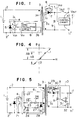
- Fig. 1 is a circuit diagram of one embodiment of a switching power supply of the invention.
- the DC power supply 1 the input terminals 2, 2', the transformer 3 having the primary winding 3a, secondary winding 3c and the bias winding 3b, the switching element 4 as the first switching means, the rectifying diode 7, the smoothing capacitor 9, the output terminals 11, 11', and the diode 5.
- this diode 5 allows the current in the primary winding 3a to flow therein even if the switching element 4 is in the off-state.
- this diode 5 has its anode connected to the input terminal 2' and its cathode connected to one end of the primary winding 3a so that it is connected in parallel with the switching element 4.
- Shown at 6 is the synchronizing oscillation circuit which renders the switching element 4 to turn on in a predetermined on-period and to turn off until the induced voltage in the winding 3b is reversed in its polarity. The repetition of the on-and off-operations makes the oscillation continue.
- a second switching element as the second switching means.
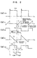
- Figs. 2 at (a) is shown the voltage waveform V os across the switching element 4, at (b) the primary current I ⁇ flowing in the primary winding 3a, at (c) the drive pulse waveform V G1 from the synchronizing oscillation circuit 6, at (d) the secondary current waveform 1 0 flowing in the secondary winding 3c, at (e) the drive pulse waveform V G2 to the secondary switching element 8 wherein the shaped area in the off-period shows the reverse current period in which the secondary current is flowed in the secondary winding 3c.
- the primary current flows in the primary winding 3a to generate magnetic flux in the transformer 3, thereby storing energy therein.
- a voltage is induced in the secondary winding 3c of the transformer 3, reverse biasing the rectifying diode 7, and the secondary switching element 8 is turned off.
- the switching element 4 is turned off by the off-signal from the synchronizing oscillation circuit 6, a flyback voltage is induced in the primary winding 3a and at the same time a flyback voltage is caused in the secondary winding 3c, thereby forward-biasing the rectifying diode 7.
- the energy stored in the transformer 3 is released through secondary winding 3c in the form of secondary current and smoothed by the smoothing capacitor 9, thus appearing as an output between the output terminals 11, 11'.
- the secondary switching element 8 is turned on by the control circuit 10, the secondary current in either element does not cause any trouble in operation.
- the energy stored in the transformer 3 is all released so that the secondary current becomes zero, the voltage across the smoothing capacitor 9, or the output voltage is supplied through the secondary switching element 8 already in the on-state, to the secondary winding 3c, so that the secondary current is flowed from the smoothing capacitor 9 in the reverse direction, generating magnetic flux in the reverse direction to store energy in the transformer 3.
- the control circuit 10 controls the secondary switching element 8 to be in the on-state.
- the voltage induced in each winding of the transformer 3 is reversed in its polarity, so that the voltage induced in the secondary winding 3c reverse-biases the rectifying diode 7.
- the secondary switching element 8 since the secondary switching element 8 is in the off-state, current is not flowed in the secondary winding, and the induced voltage in the primary winding 3a is in the direction in which a negative voltage is applied to the connection point between the switching element 4 and one end of the primary winding and a positive voltage to the connection point between the input terminal 2 and the other end of the winding.
- the primary current flows through the diode 5 to charge the DC power supply 1 so that the energy stored in the transformer 3 during the off-period is released back to the DC power supply 1.
- the synchronizing oscillation circuit 6 turns the switching element 4 on, and in this case the primary current in either element does not cause any trouble in operation.
- Fig. 2 shows operating waveforms.
- the off-period t1 to t3 of the drive pulse waveform V G1 from the synchronizing oscillation circuit 6 is represented by TOFF, the reverse current period (t2 to t3) of the secondary current 1 0 thereof by T OFF' , the on-period (t3 to t5) by T ON and the released-back period (t3 to t4) of the primary current I D thereof by T ON' .
- the output current I OUT from the output terminals 11, 11' is expressed as The output voltage V OUT is given as
- the oscillation frequency f is expressed as where N s is the number of turns of the secondary winding 3c, Np is the number of turns of the primary winding 3a, L s is the inductance value of the secondary winding 3c, V IN is the input voltage supplied from the DC power supply 1, T ON is the on-period of the switching element 4, TOFF is the off-period of the switching element 4 and T is the oscillation period.
- the off-period TOFF is constant and the oscillation frequency is constant as long as the V OUT is constant.
- the reverse current period ToFF can be changed by the secondary switching element 8 which is controlled by the control circuit 10.
- the control circuit 10 controls the on-period of the secondary switching element 8, thereby changing the reverse current period ToFF so that the output voltage V OUT is controlled to be constant at all times.
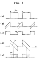
- Fig. 3 shows operating waveforms with the output current l OUT changed
- Fig. 4 shows the B-H curve for indicating the magnetic flux change in the transformer 3 at that time.
- the solid line indicates the so-called maximum loading time when the maximum value of the output current l OUT is flowed from the output ends 11, 11'
- the broken line indicates the so-called no-loading time when the output current I OUT is zero.
- the solid line indicates the magnetic flux change at the time of the no-load. Since the T oN -period and ToFF-period are constant under constant input voltage even if the output current is changed, the magnetic flux change width, ABY is always constant.
- Fig. 5 shows another embodiment of this invention.
- like elements corresponding to those in Fig. 1 are identified by the same reference numerals and will not be described.
- a secondary bias winding 3d wound on the secondary winding 3c of the transformer 3 bipolar transistors (hereinafter, abbreviated BPT) 21, 23 and 30, resistors 22, 25, 27 and 29, capacitors 24 and 26, a diode 28, an error amplifier 31, and a reference voltage 32.
- the BPT 21 is used as the switching element 4
- the BPT 30 as the second switching element 8.
- the circuits constituting the synchronizing oscillation circuit 6 are operated as described below.
- the induced voltage in the biasing winding 3b causes the drive current to flow through the series circuit of the resistor 25 and the capacitor 26 to the BPT 21, thus the BPT 21 being maintained in the on-state.
- the induced voltage in the bias winding 3b which is proportional to the input voltage charges the capacitor 24 through the resistor 27, increasing the voltage across the capacitor 24.
- This voltage drives the base of the BPT 23, turning the BPT 23 on so that the BPT 21 is turned off since the base of the BPT 21 is shorted.
- a flyback voltage proportional to the output voltage induced in the bias winding 3b in the off-period of the BPT 21 charges the capacitor 24 through the diode 28.
- the resulting voltage across the capacitor 24 reverse-biases the base of the BPT 23.
- the capacitor 24 is reversely charged until forwardly biasing the base of the BPT 23. Therefore, the on-period is determined by a period until the BPT 23 is turned on, and maintained substantially constant although it is slightly changed by the input voltage and output voltage.
- a flyback voltage is induced in the secondary bias winding 3d in the off-period of the BPT 21, and supplied through the resistor 29 to the base of the BPT 30, turning it on.
- the energy stored in the transformer 3 during the on-period is released through the second winding 3c as the secondary current during the off-period.
- the secondary current flows through the BPT 30 already in the on state, from the capacitor 9 into the secondary winding 3c in the reverse direction.
- the base current I B to the BPT 30 is from the error amplifier 31 which detects the output voltage and compares it with the reference voltage 32, the secondary current 1 0 ' is limited to a value determined by the equation,
- the BPT 30 swiftly turns off and at the same time the polarity of the induced voltage in each winding of the transformer 3 is inverted, so that a voltage is induced in the bias winding 3b to forward-bias the base of the BPT 21, again turning on the BPT 21. Repetition of the above operations maintains the oscillation continue, controlling the output voltage.
- the resistor 22 supplies a small current to the base of the BPT 21, to actuate it to start.
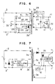
- Fig. 6 shows still another embodiment of this invention.
- the switching element 45 and the secondary switching element 8 in Fig. 5 are formed of field effect transistors (hereinafter, abbreviated FET). Since this embodiment utilizes the body diode parasitically built in the FET, it does not include the diode 5 and the rectifying diode 7. The operation of this embodiment is the same as that of Fig. 5, and thus will not be described. Shown at 33 and 34 are FETs. The resistor 22 supplies a voltage to the gate of the FET 33, thereby starting it.
- FET field effect transistors
- Fig. 7 shows further embodiment of this invention.
- a feed-back winding 3e is separately provided on the transformer 3 shown in Fig. 1.
- the energy stored in the transformer 3 through the secondary winding 3c of the transformer 3 is released to the output terminal 11, 11', and the series circuit of the feed-back winding 3e, diode 35 and secondary switching element 8 supplies output voltage.
- energy is again stored in the transformer 3 and released back to the DC power supply 1 through the primary winding 3a of the transformer 3.
- the operation of this embodiment is the same as in Fig 1 and will not be described.
- the number of turns of the secondary winding 3c must be equal to or smaller than that of the feed-back winding 3e.
- the diode 35 can be omitted.
- Fig. 8 shows still further embodiment of this invention.
- a multiple output winding 3f is additionally provided on the transformer 3 shown in Fig. 1 to increase the output terminal number.
- a second output voltage rectified and smoothed through a rectifying diode 36 and a smoothing capacitor 37 connected to the multiple output winding 3f is supplied through output terminals 38, 38'.
- the operation is the same as in Fig. 1 and will not be described.
- more separate windings can be provided similarly as above.
- Fig. 9 shows further embodiment of this invention.
- the synchronizing oscillation circuit 6 in Fig. 6 is replaced by a separately excited oscillation circuit 39, and the bias winding 3b is removed from the transformer 3.
- the separately excited oscillation circuit 39 repeats on and off operations at a predetermined constant frequency and drives the switching element 4.
- like elements corresponding to those in Fig. 1 are identified by the same reference numerals and will not be described.
- the operation of this invention will be described with reference to Figs. 9 and 10.
- like elements corresponding to those in Fig. 2 are identified by the same reference numerals and will not be described.
- the energy stored in the transformer 3 during the on-period (t15 to t16) of the separately excited oscillation circuit 39 is to cause the following periods.
- the off-period t11 to t15 of the separately excited oscillation circuit 39 includes the period ToFF, (t11 to t12) in which part of the stored energy is released through the secondary winding 3c of the transformer 3 to the output voltage, the reverse current period T OFF2 (t12 to t13) in which the output voltage is supplied through the secondary switching element 8 to the secondary winding 3c of the transformer 3, the released-back period TOFF3 (t13 to t14) in which the energy stored in the transformer 3 through the primary winding 3a during the reverse current period T OFF2 is released back to the DC power supply 1, and the dead period T OFF4 (t14 to t15) in which no magnetic flux is generated in the transformer 3 and the voltage across the switching element 4 is the same as the input voltage V IN of the DC power supply 1.
- the output voltage is controlled by the same operation as in Fig
- Fig. 11 shows further embodiment of this invention.
- the input-output insulation arrangement shown in Fig. 1 is replaced by a non-insulation arrangement, or the so-call back boost converter. The operation is the same as that in Fig. 1 and will not be described.
- Shown at 40 is a choke transformer which is formed of a main winding 40a and a bias winding 40b.
- a current is flowed from the input to the main winding 40a to store energy in the choke transformer 40.
- the bias winding 40b provides the on-state timing to the synchronizing bias winding 40b.
- the T oN -period against the overcurrent of output current the T oN -period is always fixed to a constant value which is predetermined by the synchronizing circuit 6 and the separately excited oscillation circuit 39.
- the maximum output current is automatically limited, but changed with the change of input voltage.
- by changing the T oN -period in reverse proportion to the input voltage it is possible to make the maximum output current constant against the over-current of output current.
- the secondary switching element 8 is turned on in synchronism with the turning off of the switching element 4, the secondary current is all flowed to the switching element 8, thus no rectifying diode 7 is required.
- the synchronizing oscillation circuit 6 is turned on in synchronism with the turning off of the switching element 8, no diode 5 is required.
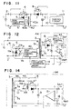
- Fig. 12 shows further embodiment of this invention.
- like elements corresponding to those in Fig. 24 are identified by the same reference numerals and will not be described.
- Shown at 41 is a capacitor connected to the switching element 4, 42 a synchronizing oscillation control circuit, 43 a control circuit which determines the reverse current period in which the secondary current is flowed in the secondary switching element 8, and 44 a secondary side control block.
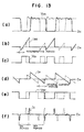
- Fig. 13 In Fig. 13, at (a) is shown the voltage waveform V os across the switching element 4, at (b) the current waveform I DS flowing in the switching element 4 and diode 5, at (c) the drive pulse waveform V GI to the synchronizing oscillation control circuit 42, at (d) the secondary current waveform 1 0 flowing in the secondary winding 3c, at (e) the drive pulse waveform V G2 from the control circuit 43, and at (f) the current waveform l c flowing through the capacitor 41.
- the secondary current released through the secondary winding 3c decreases to zero, a voltage across the smoothing capacitor 9, or the output voltage is supplied through the secondary switching element 8 which is already in the on-state, to the secondary winding 3c. Consequently, the secondary current flows from the smoothing capacitor 9 in the reverse direction toward the secondary winding c, so that magnetic flux is produced in the transformer 3 in the opposite direction to that mentioned above, or that energy is stored in the transformer.
- the control circuit 43 controls the reverse current period in which the secondary current is flowed in the reverse direction, and when the secondary switching element 8 is turned off, the polarity of the voltage induced in each winding of the transformer 3 is reversed.
- the voltage induced in the secondary winding 3c reverse-biases the rectifying diode 7 and turns off the secondary switching element 8
- the voltage induced in the primary winding 3a is in the direction in which the negative voltage is applied to the connection point between the capacitor 41 and the one end of the primary winding 3a and the positive voltage to the connection point between the input terminal 2 and the other end of the primary winding 3a. Therefore, the charge stored in the capacitor 41 is discharged, and thus the primary current is flowed to charge the DC power supply 1, or the energy stored in the reverse current period is released back to the power supply 1.
- the synchronizing oscillation control circuit 42 detects the current flowing in the diode 5 and turns on the switching element 4, but since the voltage across the capacitor 41 is already zero in the released-back period, no loss is caused when the switching element 4 is turned on, or the so-called zero-cross switching is brought about.
- the reverse current period ToFF 43 in Fig. 12 is selected to be a value at which the voltage across the capacitor 41 can be completely reduced to zero during the regenerative period T ON ' by discharge, and thus it is fixed or made variable by the capacitance value, input voltage and flyback voltage.
- the capacitor 41 connected across the switching element 4 prevents the rapid increase of voltage when the switching element 4 turns off, thus decreasing the turn-off loss.
- the spike voltage generated by the leakage inductance of the transformer 3 is absorbed, the voltage to be applied is low.
- the zero-cross switching is brought about, causing no turn-off loss.
- the charge stored in the capacitor 41 and the energy restored in the transformer 3 in the reverse-current period are all released-back to the DC power supply 1, almost no loss is caused and, since the steep change of voltage waveform can be prevented, the switching noise is greatly reduced.
- Fig. 14 shows a specific circuit arrangement of the secondary-side control circuit 43 of the embodiment of this invention in Fig. 12.
- like elements corresponding to those in Fig. 12 are identified by the same reference numerals and will not be described.
- a drive winding one end of which is connected to the secondary winding 3c of the transformer 3, and the other end of which is connected to the base of a BPT 47 through a resistor 46.
- the BPT 47 has its collector connected to the cathode of the diode 7 and its emitter connected through a resistor 49 to the anode of the diode 7.
- Shown at 48 is a BPT which has its base connected to the connection point between the resistor 49 and the emitter of the BPT 47, its collector connected to the connection point between the resistor 46 and the base of the BPT 47, and its emitter connected to the connection point between the diode 7 and the resistor 49.
- Fig. 14 The operation of the embodiment of Fig. 14 is the same as that described with reference to Fig. 5. That is, when the switching element 4 is turned off, part of the energy stored in the transformer 3 is released through the secondary winding 3c to the output terminals 11, 11' as the secondary current. At this time, a voltage is induced in the drive winding 3e to flow a drive current through the resistor 46 to the base of the BPT 47, thus turning the BPT 47 on. However, almost all the secondary current released from the secondary winding 3c is flowed in the diode 7. When the energy stored in the transformer is released, the output voltage V OUT is applied through the resistor 49 and the BPT 47 which is already on, to the secondary winding 3c.
- Fig. 15 shows further embodiment of this invention.
- like elements corresponding to those in Fig. 12 are identified by the same reference numerals and will not be described.
- Shown at 52 is a capacitor, which is connected across the rectifying diode 7 so as to absorb the spike voltage generated by the leakage inductance of the secondary winding 3c and primary winding 3a of the transformer 3 which voltage is applied thereacross when the secondary switching element 8 is turned off.
- the secondary switching element 8 is turned on and off by a secondary synchronizing oscillation control circuit 53.
- the secondary synchronizing oscillation circuit 53 generates a drive on-off signal to the secondary switching element 8, detects that current is flowed in the rectifying diode 7, and detects the current in the secondary switching element 8 so as to maintain the current to flow until the current flowing from the secondary winding 3c to the output terminal 11' exceeds a constant value.
- the operation of the embodiment of Fig. 15 as to the secondary winding side is the same as that in the primary winding side of the embodiment of Fig. 12. Since the capacitors 41, 52 are respectively connected on the primary and secondary winding side of the transformer 3, they absorb the spike voltages induced in the primary winding 3a and secondary winding 3c due to the leakage inductance of the transformer 3 and simultaneously prevents abrupt increase of the induced voltage, so that the switching noise caused in the primary winding 3a and secondary winding 3c of the transformer 3 can be reduced further. Moreover, since the energy absorbed and stored in the capacitors 41, 52 are all released back, or recovered to the input and output, no loss is produced. Also, since the zero-cross switching is brought about when the switching element 4 and the secondary switching element 8 are turned on, the turn-on loss is not caused, and since the abrupt increase of the applied voltage is prevented upon turning-off, the turn-off loss can be reduced.
- the control circuit 43 and the secondary synchronizing oscillation control circuit 53 are operated to maintain the secondary current flowing the secondary switching element 8 constant, the output voltage control may be performed as in Fig. 1, and in this case the insulating transmission means 14 can be omitted.
- Fig. 16 shows still further embodiment of this invention.
- like elements corresponding to those in Figs. 1 and 26 are identified by the same reference numerals.
- Shown at 3f is a secondary winding which is wound on the transformer 3 and supplies the output voltage to the output terminals 62, 62' through the rectifying diode 60 and smoothing capacitor 61.
- Shown at 63 is a control circuit which determines the revers current period in which the secondary current is flowed in the secondary switching element 8, and at 64 is a non-control output block.
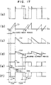
- Fig. 17 at (a) is shown the voltage waveform V os across the switching element 4, at (b) the primary current I D flowing in the primary winding 3a, at (c) the secondary current waveform 1 02 flowing in the secondary winding 3f, at (d) the secondary current waveform 1 02 flowing in the secondary winding 3c, at (e) the drive pulse waveform V G1 from the synchronizing oscillation control circuit 13, at (f) the drive pulse waveform V G2 to the secondary switching element 8 to be controlled by the control circuit 63, in which the shaded area is the reverse current period in which the secondary winding 3c in the off-period. Also in Fig.
- the solid line shows that the output current I OUT2 is much flowed from the output terminals 11, 11' and the broken line indicates that the output current I OUT2 is a little flowed from the output terminals 11, 11'.
- the output current I OUT1 flowing out of the output terminals 62, 62' is constant.
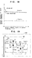
- Fig. 18 is a graph of the output voltages V OUT1 and V OUT2 relative to the output current I OUT2 at the output terminals 11, 11' with the output current I OUT1 at the output terminals 62, 62' made constant.
- the solid line indicates the output characteristic according to this invention and the broken line indicates the characteristic in the prior art.
- the output voltage V OUT1 is not changed because it is always controlled in both invention and prior art.
- the energy supplied from the secondary winding 3c of the tranformer 3 is used as output current I OUT2 from the output terminals 11, 11' and also, part thereof is used as the current flowing in the secondary winding 3c through the secondary switching element 8 only during the reverse current period.
- the output current I OUT2 flowing out of the output terminal 11, 11' is stopped due to no load, the current during the reverse current period is always used, and thus equivalently a load is connected to bring the bleeder current l our2 as expressed by where LS2 is the inductance of the secondary winding 3c and ToFF is the reverse current period.
- the bleeder current l' OUT2 can be adjusted by changing the reverse current period T'OFF by the control circuit 63, and if necessary the bleeder current l' OUT 2 can be set.
- the current flowing in the secondary winding 3c in the reverse current period, or the bleeder current l' OUT 2 is stored in the transformer 3 in the form of energy and, when the second switching element 8 is turned on, it is released through the primary winding 3a back to the DC power supply 1. Thus, no loss is produced.
- the relation between the reverse current period ToFF and the release back period T ON ' is given as
- Fig. 19 shows another specific circuit arrangement of the non-control output block 64 in the embodiment of this invention shown in Fig. 16.
- Fig. 19 at 71 is shown a diode, at 65 and 68 are Zener diodes.
- At 66, 68 and 69 are resistors and at 67 is a BPT.
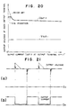
- Fig. 20 is a graph of the output voltage V ouT 2, showing the stabilized situation of the output voltage.
- the output voltage V ouT 2 can be set to an increase value by changing the Zener voltage of the Zener diode 70. If the output voltage V ouT 2 is smaller than the Zener voltage, no reverse current period is present and no bleeder current flows so that the output power corresponding to the bleeder current can be prevented from increase.
- the output voltage is stabilized by controlling the on-and off-periods of the switching element 4, the input voltage from the DC power supply 1 may be controlled by a regulator or the like for the stabilization of the output voltage.
- a detection winding may be separately provided on the transformer 3 to produce a voltage same as the output voltage which detection winding voltage is controlled to be constant, or the so-called tertiary winding control system may be employed to stabilize the output voltage.
- the on-period can be fixed to control the output voltage to be constant against the variations of the input voltage and output current, and the oscillation frequency variation can be greatly reduced.
- the oscillation frequency is fixed, enabling high frequency operation and miniaturization of transformer and secondary rectifying and smoothing circuits.
- the attenuation frequency band region of the noise filter can be narrowed, resulting in small size and low cost.
- the transient variation of the output current can be removed.
- the control range is the same as in the prior art, the turn-on and turn-off loss of the switching element can be greatly decreased, and at the same time the spike voltage and spike current to be supplied to the switching element can be greatly reduced.
- the switching noise occurring in the primary and secondary winding sides of the transformer can be decreased, it is possible to produce a switching power supply with high frequency, low noise and good high frequency performance.
- the output voltage under a light load in the un- controlled output can be prevented from increase by a relatively simple circuit, the stability of the uncontrolled output can be greatly improved, and the bleeder current for prevention against light load is flowed through the primary winding back to the DC power supply, thus resulting in almost no loss and high efficiency in the switching power supply.
Landscapes
- Engineering & Computer Science (AREA)
- Power Engineering (AREA)
- Dc-Dc Converters (AREA)
Description
- This invention relates to a switching power supply for supplying DC stabilized voltages to industrial and consumer equipments.
- The conventional switching power supply has such an arrangement as shown in Fig. 22. In Fig. 22, there is shown a
DC power supply 1 which is obtained by rectifying and smoothing an AC voltage or formed of a battery. This DC power supply is connected betweeninput terminals 2, 2' so as to supply a positive voltage to theinput terminal 2 and a negative voltage to the input terminal 2'. Shown at 3 is a transformer which has one end of aprimary winding 3a connected to theinput terminal 2, the other end thereof connected through aswitching element 4 to the input terminal 2', one end of asecondary winding 3c connected to an output terminal 11', the other end thereof connected through adiode 7 to an output terminal 11, one end of a bias winding 3b connected to the input terminal 2', and the other end thereof connected to a synchronizingoscillation control circuit 13. Theswitching element 4 is turned on and off when supplied at its control terminal with an on-off signal from the synchronizingoscillation control circuit 13, thereby interrupting the input voltage to theprimary winding 3a. The synchronizingoscillation control circuit 13 controls to change the on-period of theelement 4 by the output signal from insulating transmission means 14 such as photocouplers and keeps the off-state until the voltage across the bias winding 3b is reversed in its polarity. The rectifyingdiode 7 has its anode connected to one end of the secondary winding 3c and its cathode connected to the output terminal 11. Shown at 9 is a smoothing capacitor, which is connected between the output terminals 11, 11'. The rectifyingdiode 7 rectifies the voltage induced in thesecondary winding 3c connected between the output terminals 11, 11' and thesmoothing capacitor 9 acts to smooth the rectified voltage and to supply it to the output terminals as the output voltage. Shown at 15 is an error amplifier which compares areference voltage 16 and the output voltage between the output terminals 11, 11', amplifies the compared signal and supplies it to the insulating transmission means 14. The insulating transmission means 14 acts to insulate between the primary and secondary windings and to transmit the signal from theerror amplifier 15 to the synchronizingoscillation control circuit 13. The operation of this conventional example will be described below. - The input voltage supplied from the
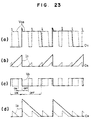
DC power supply 1 which is connected between theinput terminals 2, 2', when theswitching element 4 is turned on by the on-signal from the synchronizingoscillation control circuit 13, is supplied across theprimary winding 3a of thetransformer 3 in the on-period to allow a primary current to flow in the primary winding, this causing magnetic flux in thetransformer 3 to that energy is stored in thetransformer 3. At this time, a voltage is induced in the second winding 3c of thetransformer 3 so as to bias the rectifyingdiode 7 in the reverse direction. When theswitching element 4 is turned off by the off-signal from the synchronizingoscillation control circuit 13, a flyback voltage is generated in theprimary winding 3a and at the same time, another flyback voltage is generated in thesecondary winding 3a so as to forward-bias the rectifyingdiode 7. Therefore, the energy stored in thetransformer 3 is released in the form of a secondary current in the secondary winding 3c. This current is rectified by thesmoothing capacitor 9 to produce the output voltage which appears between the output terminals 11, 11'. When the energy stored in thetransformer 3 is all released out, the flyback voltages in the primary andsecondary windings transformer 3, and tends to change to the polarity opposite to that of the flyback voltage. The change of polarity is transmitted to the synchronizingoscillation control circuit 13, again turning on theswitching element 4. Repetition of these operations provides a continuous output voltage from the terminals 11, 11'. - Moreover, the operation in which the output voltage is controllably stabilized will be described in detail with reference to Fig. 23. Shown in Fig. 23 at (a) is a voltage waveform VDs across the
switching element 4, at (b) is a primary current ID which flows in theprimary winding 3a, at (c) is a drive pulse waveform VG from the synchronizingoscillation control circuit 13 and at (d) is a secondarycurrent waveform 10 which flows in thesecondary winding 3c. In this figure, the solid lines indicate a so-called over-load time in which a large amount of output current lOUT flows out of the output terminals 11, 11', and the broken lines indicate a so-called light-load time in which a small amount of output current lOUT flows out of the terminals. In general, the current lOUT is expressed by


secondary winding 3c, Np is the number of turns of theprimary winding 3a, Ls is the inductance of thesecondary winding 3c, VIN is the input voltage supplied from theDC power supply 1, TON is the on-period of theswitching element 4, TOFF is the off-period of theswitching element 4 and T is the oscillation period. - The output voltage VOUT is compared with the
reference voltage 16 in theerror amplifier 15 and the compared result is supplied through the insulation transmission means 14 to the synchronizingoscillation control circuit 13, thereby controlling the on-period of theswitching element 4. Therefore, the output voltage is always controlled to be constant with the on-period changed even though the output current lOUT and the input voltage VIN are changed. Fig. 23 shows such situations. However, since the change of the on-period results in the change of the off-period, the oscillation frequency f is also changed as is obvious from the figure. Moreover, in order to prevent the on-period from being increased without limit by an over-current due to short-circuiting of the output terminals 11, 11' or the like, it is necessary that the synchronizingoscillation control circuit 13 has the function of limiting the maximum on-period or the primary current. - In the conventional switching power supply shown in Fig. 22, however, the voltage and current waveforms to be supplied when the
switching element 4 is turned on and off are simultaneously changed while crossing each other due to the gradients depending on the response speed of theswitching element 4, thus causing a large switching loss. In addition, if the switching loss is decreased by increasing the response speed of theswitching element 4, the voltage and current waveforms become steeper, leading to increase of the switching noise and the voltage and current spikes which are supplied to theswitching element 4. - Recently, to solve such problems, various resonant-type switching power supplies utilizing LC resonance are proposed in which an inductance and capacitance are inserted on the switching circuit.
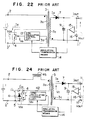
- Fig. 24 shows an arrangement of a conventional resonant-type switching power supply. In Fig. 24, like elements corresponding to those in Fig. 22 are identified by the same reference numerals and will not be described. Referring to Fig. 24, there are shown an
inductance 45 which is connected in series between theinput terminal 2 and theprimary winding 3a of thetransformer 3, and acapacitor 41 which is connected in parallel with theswitching element 4. Theseinductance 45 and thecapacitance 41 constitute an LC resonant circuit. Shown at 5 is a diode which is connected across theswitching element 4. This diode has its anode connected to the input terminal 2' and its cathode connected one end of theprimary winding 3a, so that when the energy stored in theinductance 45 is released bach to theDC power supply 1, a current can be flowed in the winding even under the off-state of theswitching element 4. Shown at 42 is a synchronizing oscillation control circuit which generates an on-off control signal to theswitching element 4 and detects the current in thediode 5 so that the on-period of theswitching element 4 is changed and the off-period is maintained until a current flows in thediode 5. - Fig. 25 shows a operating waveforms at each portions. In Fig. 25, at (a) is shown the voltage waveforms VDS across the
switching element 4, at (b) a current waveform I'os which flows in theswitching element 4 and in thediode 5, at (c) a drive pulse waveform VG1 from the synchronizingoscillation control circuit 42, at (d) a current waveform I'c flowing in thecapacitor 41, at (i) a secondarycurrent waveform 10 flowing in thesecondary winding 3c, and (j) an induced voltage waveform Vo across thesecondary winding 3c. As will be understood from the operating waveforms, energy is stored in thetransformer 3 andinductance 45 in the on-period of theswitching element 4, while in the off-period, the energy stored in thetransformer 3 is released through thesecondary winding 3c to the output terminals 11, 11' and the energy stored in theinductance 45 is released to charge thecapacitor 41. As a result, a sine-wave voltage vibrating at a resonant frequency,
inductance 45 and the capacitance value c of thecapacitor 41, is generated across thecapacitor 41. Moreover, the vibrating sine wave voltage vibrates about the sum of the input voltage of theDC power supply 1 and the flyback voltage induced in theprimary winding 3a. Thus, the values of theinductances 45 andcapacitor 41 and the on-period are set so that the amplitude becomes much larger than the sum of the input voltage and the flyback voltage, causing the voltage across thecapacitor 41 to be negative. This negative-voltage period causes the voltage across thecapacitor 41 to be zero and a current is flowed in theinductance 45 through thediode 5. At this time, theswitching element 4 is turned on by the synchronizingoscillation control circuit 42, but no discharge current is flowed from thecapacitor 41 to theswitching element 4, thus the so-called zero-cross switching being caused in which the switching element is in the on-state with zero voltage applied there across. This operation is repeated to supply the output voltage to the output terminals 11, 11'. In this resonant-type switching power supply, the voltage waveform (current waveform or both voltage and current waveforms depending on the system) applied when theswitching element 4 is turned on and turned off gently changes with a sine-wave gradient irrespective of the response speed of theswitching element 4. Thus, even if the current waveform is abruptly changed, the switching loss is small and since the voltage waveform is a sine wave, the switching noise is very little. In this resonant-type switching power supply, however, when theswitching element 4 is turned on, the above zero-cross switching must be made, otherwise thecapacitor 41 would be shorted through theswitching element 4, thus breaking theswitching element 4, or the switching loss would be suddenly increased or the switching noise would be increased. Therefore, it is very difficult to control the output voltage to be always constant against a wide range of input voltage and output current variations while the zero-cross switching is being secured. Also, other effective means have not yet been found so far. In other words, the minimum value of the on-period is limited for assuring the zero-cross switching and the off-period TOFF is also limited since the resonant frequency fc is maintained to be constant for assuring the zero-cross switching, or the off-period
must be restricted in the range of
switching element 4 is rectangular, but in the resonant-type it is a sine wave, so that the peak value of the applied waveform increases. This follows that theswitching element 4 is required to have a large capacity and that a large resonant current is flowed through theinductance 45,capacitor 41 and primary winding 3C to theDC power supply 1. - Moreover, Fig. 26 shows another conventional switching power supply arranged to have a plurality of secondary windings in the
transformer 3 and rectifying and smoothing means provided in each of the secondary windings, thereby generating a plurality of output voltages. In Fig. 26, like elements corresponding to those in Fig. 22, are identified by the same reference numerals and will not be described. In Fig. 26, there is shown a secondsecondary winding 3f would on thetransformer 3. This secondary winding has its one end connected to an output terminal 62' and its other end connected to anoutput terminal 62 through a rectifyingdiode 60. There is also shown acapacitor 61 which is connected between theoutput terminals 62, 62' and serves to smooth the induced voltage in thesecondary winding 3f and to supply the output voltage. - The operations of the
error amplifier 15,reference voltage 16, insulation transmission means 14, and synchronizingoscillation control circuit 13 by which theoutput voltage V OUT 1 between the output terminals 62-62' is controlled to be stabilized have been mentioned with reference to Figs. 22 and 23 and thus will not be described again. Theoutput voltage V OUT 2 between the output terminals 11, 11' which is not directly controlled, or an un-controlled output is a voltage proportional to thevoltage output VOUT 1, or is expressed as
output voltage V OUT 2 is not sufficiently high because the output current causes voltage drops chiefly across the impedance of the secondary winding, the operating impedance of the rectifying diode and the leakage inductance between thesecondary windings - In this conventional arrangement of Fig. 22, in order to control the output voltage to be constant against the variations of the input voltage and output current, it is necessary to greatly change the oscillation frequency. However, since the upper limit of the oscillation frequency is determined by the operating frequency of the
switching element 4, the response of the synchronizingoscillation control circuit 13 and of the control system and so on, the lower limit of the oscillation frequency must inevitably be lowered to widen the control range. Thus, thetransformer 3 and the rectifying and smoothing circuits in the secondary winding, since they are designed for the lowest oscillation frequency, become large in their size and capacity, thus making the power supply be large-sized to be expensive. In addition, since the control loop responds late to the transient variations of the output current, the output voltage has a transient variation. Particularly when the output voltage is transiently increased, the charge on the smoothingcapacitor 9 is discharged through the output terminals 11, 11' in the form of the output current. Therefore, the discharge speed is slow when the output current is small, and hence it takes a long time for the output voltage to be stabilized, or the response of the output voltage to be transient change is very poor. Moreover, in order to protect the short circuit between the output terminals and the output current from over-current, it is necessary to provide a circuit for limiting the maximum value of the on-period. Also, for the insulation between the primary and secondary windings the insulation transmission means 14 such as a photocoupler is required to transmit a control signal. These requirements make the circuit arrangement complicated to increase the cost. Moreover, in order to reduce the switching loss occurring when the switchingelement 4 is turned on and off thereby to make the high frequency operation possible, the response speed of theswitching element 4 must be increased, thus the switching noise being increased. Consequently, the noise filter to be inserted in the input and output terminals for the purpose of preventing equipment from interfering with noise becomes large-sized. In addition, since the surge voltage and current to be applied to theswitching element 4 are increased, a switching element of which capacity is excessively large is required. To solve these problems, if the rapid change of the turn-off waveform is suppressed, the turn-off loss and snubber-circuit loss increased, thus lowering the efficiency to an impractical extent. Another method for reducing both the switching loss and the switching noise at a time, or such resonant-type switching power supply as shown in Fig. 24 has been proposed, but has a difficulty in the stabilizing control of the output voltage to achieve the zero-cross switching. Also, since the voltage waveform or current waveform to be applied to theswitching element 4 is a sine wave which increases the peak value, the switchingelement 4 must have a large capacity and thus cannot be improved much in the efficiency due to a large resonant current. - Moreover, the switching noise is caused not only in the primary winding of the transformer, but also in the secondary winding. The switching noise in the secondary winding is large which is caused by the generation of ringing waveform due to the distributing capacitance between the leakage inductance (between the secondary winding and the primary winding as viewed from the secondary winding side) and the secondary winding, and by the recovery current of the rectifying diode, chiefly when the switching
element 4 is turned off. To cope with these problems, a snubber circuit is connected across the secondary winding or the rectifying diode as in the primary winding. However, the snubber-circuit loss is increased and the current flowing in the snubber circuit is transmitted from the secondary winding of the transformer to the primary winding thus increasing the spike current to cause a large loss when the switchingelement 4 is turned off. - In the conventional arrangement having a plurality of secondary windings shown in Fig. 26, the detected and controlled outputs of the multiple outputs are always controlled to be stabilized, but the other un- controlled outputs are much affected by the variations of the output currents so as to slightly change. Particularly at the time of light load when the output current of the un-controlled output becomes small, inadequate coupling of the secondary winding of the transformer which contributes to the controlled output, to the other secondary windings which are associated with the un-controlled outputs will cause the un- controlled output to be easily affected by the spike voltage produced from the leakage inductance of the transformer so that the output voltage of the un-controlled output is greatly increased. In this case, the greater the output current of the controlled output and the less the output current of the un-controlled output, the more the output voltage of the un-controlled output will increase. In order to prevent the output voltage from increasing at the time of light load on the uncontrolled output, a resistor or the like is connected between the output terminals of the uncontrolled output so that a bleeder current flowing therein does not cause light load, or a regulator circuit is connected before the output. However, the bleeder current and the regulator circuit cause losses, thus lowering the efficiency of the switching power supply.
- European patent specification EP-A-13332 discloses a switching power supply including first switching means (S1) connected in series to a primary winding of a transformer (Ue), a rectifying diode (D2) connected in series to a secondary winding, second switching means (S2) connected in parallel with the rectifying diode (D2), and a control circuit (SE, PBM, PI, GG) for controlling the first and second switching means (S1, S2), and the current is enabled to flow bidirectionary from the input to the output and from the output to the input.
- IEEE Transactions on Magnetics, Vol. 1 MAG-13, No. 5, September 1977, pp 1211-1213 discloses a switching power supply including first switching means (Tri) connected in series to a primary winding (L) of a transformer, a rectifying diode (D2) connected in series to a secondary winding (n2L), second switching means connected in parallel with the rectifying diode (D2), so that the first and second switching means (Tri, Tr2) alternately perform opening and closing operations.
- It is an object of the invention to improve the transient response of the output voltage and reduce the size and cost of a switching power supply.
- It is another object of the invention to permit the switching power supply to stably operate at high frequencies, switching loss to be reduced and also switching noise to be decreased.
- It is still another object of this invention to reduce the loss in the multiple outputs having a plurality of secondary windings, thus suppressing the output voltage from increasing at the time of light load on the uncontrolled output so that the switching power supply can be operated with a high efficiency.
- According to one typical aspect of this invention, there is provided a switching power supply comprising a transformer having a primary winding and first secondary winding, first switching means adapted to turn on and off for connecting and disconnecting an input voltage to said primary winding, a diode connected in parallel with said first switching means, first rectifying and smoothing means connected across said first secondary winding, and second switching means, operating to turn on and off alternatively with said first switching means, for connecting and disconnecting an output voltage of said first rectifying and smoothing means to said first secondary winding, characterised by: control circuit means for controlling said second switching means so that an on period of said second switching means is controlled in accordance with an output voltage of said first rectifying and smoothing means, in order to feed back the output voltage supplied to said first secondary winding to said primary winding.
-
- Fig. 1 is a circuit diagram of one embodiment of a switching power supply of this invention.
- Figs. 2 to 4 are waveform diagrams showing the operating waveforms in the circuit arrangement of this invention in Fig. 1.
- Figs. 5 to 9 are circuit diagrams of other embodiments of the switching power supply according to this invention.
- Fig. 10 is a waveform diagram showing the operating waveforms in the circuit arrangement of the invention in Fig. 9.
- Figs. 11 to 12 are circuit diagrams of other embodiments of the switching power supply of this invention.
- Fig. 13 is a waveform diagram showing the operating waveforms in the circuit arrangements of the invention in Fig. 12.
- Fig. 14 is a specific circuit diagram of the secondary control block of the invention shown in Fig. 12.
- Figs. 15 to 16 are circuit diagrams of other embodiments of the switching power supply of this invention
- Fig. 17 is a waveform diagram showing the operating waveforms in the current arrangement of the invention in Fig. 16.
- Fig. 18 is a graph showing the output characteristic of the power supply of the invention in Fig. 16.
- Fig. 19 is a circuit diagram of the secondary-side un-controlled block of this invention shown in Fig. 16.
- Fig. 20 is a graph showing the output characteristic of the power supply of the invention in Fig. 19.
- Fig. 21 is a diagram showing the effect of the invention.
- Fig. 22 is a circuit diagram of the conventional switching power supply.
- Fig. 23 is a graph showing the operating waveforms in the conventional circuit arrangement in Fig. 22.
- Fig. 24 is a circuit diagram of another conventional switching power supply.
- Fig. 25 is a graph showing the operating waveforms in the conventional circuit arrangement in Fig. 24.
- Fig. 26 is a circuit arrangement of still another conventional switching power supply.
- Fig. 1 is a circuit diagram of one embodiment of a switching power supply of the invention. In Fig. 1, like elements corresponding to those in Fig. 22 are identified by the same reference numerals and will not be described. Referring to Fig. 1, there are shown the
DC power supply 1, theinput terminals 2, 2', thetransformer 3 having the primary winding 3a, secondary winding 3c and the bias winding 3b, the switchingelement 4 as the first switching means, the rectifyingdiode 7, the smoothingcapacitor 9, the output terminals 11, 11', and thediode 5. When the energy stored in thetransformer 3 is released through the primary winding 3a to theDC power supply 1, thisdiode 5 allows the current in the primary winding 3a to flow therein even if theswitching element 4 is in the off-state. That is, thisdiode 5 has its anode connected to the input terminal 2' and its cathode connected to one end of the primary winding 3a so that it is connected in parallel with the switchingelement 4. Shown at 6 is the synchronizing oscillation circuit which renders the switchingelement 4 to turn on in a predetermined on-period and to turn off until the induced voltage in the winding 3b is reversed in its polarity. The repetition of the on-and off-operations makes the oscillation continue. When at 8 is a second switching element as the second switching means. After the energy stored in the transformer when the switchingelement 4 is in the on-state is released through the secondary winding 3c to the smoothingcapacitor 9 from the rectifyingdiode 7 or thesecond switching element 8 in the off-period of theswitching element 4, the secondary current is reversely flowed from the smoothingcapacitor 9 through thesecondary switching element 8 to the secondary winding 3c in a period controlled by acontrol circuit 10. Shown at 10 is the control circuit which detects the output voltage between the output terminals 11, 11', compares it with the internal reference voltage, and changes the reverse current period in which the secondary current is flowed in theswitching element 8. - The operation of the embodiment will be described in detail with reference to Figs. 1 and 2.
- In Figs. 2 at (a) is shown the voltage waveform Vos across the switching
element 4, at (b) the primary current Iα flowing in the primary winding 3a, at (c) the drive pulse waveform VG1 from the synchronizingoscillation circuit 6, at (d) the secondarycurrent waveform 10 flowing in the secondary winding 3c, at (e) the drive pulse waveform VG2 to thesecondary switching element 8 wherein the shaped area in the off-period shows the reverse current period in which the secondary current is flowed in the secondary winding 3c. During the on-period of theswitching element 4 which operates in the on-period determined by the synchronizingoscillation circuit 6, the primary current flows in the primary winding 3a to generate magnetic flux in thetransformer 3, thereby storing energy therein. At this time, a voltage is induced in the secondary winding 3c of thetransformer 3, reverse biasing the rectifyingdiode 7, and thesecondary switching element 8 is turned off. When the switchingelement 4 is turned off by the off-signal from the synchronizingoscillation circuit 6, a flyback voltage is induced in the primary winding 3a and at the same time a flyback voltage is caused in the secondary winding 3c, thereby forward-biasing the rectifyingdiode 7. Thus, the energy stored in thetransformer 3 is released through secondary winding 3c in the form of secondary current and smoothed by the smoothingcapacitor 9, thus appearing as an output between the output terminals 11, 11'. At this time, although thesecondary switching element 8 is turned on by thecontrol circuit 10, the secondary current in either element does not cause any trouble in operation. When the energy stored in thetransformer 3 is all released so that the secondary current becomes zero, the voltage across the smoothingcapacitor 9, or the output voltage is supplied through thesecondary switching element 8 already in the on-state, to the secondary winding 3c, so that the secondary current is flowed from the smoothingcapacitor 9 in the reverse direction, generating magnetic flux in the reverse direction to store energy in thetransformer 3. Since in this state the voltage induced in each winding of thetransformer 3 is not changed in its polarity, the flyback voltage in the bias winding 3b is not also changed, and thus the synchronizingoscillation circuit 6 maintains the switchingelement 4 in the off-state. Thecontrol circuit 10 controls thesecondary switching element 8 to be in the on-state. When thesecondary switching element 8 is turned off, the voltage induced in each winding of thetransformer 3 is reversed in its polarity, so that the voltage induced in the secondary winding 3c reverse-biases the rectifyingdiode 7. Also, since thesecondary switching element 8 is in the off-state, current is not flowed in the secondary winding, and the induced voltage in the primary winding 3a is in the direction in which a negative voltage is applied to the connection point between the switchingelement 4 and one end of the primary winding and a positive voltage to the connection point between theinput terminal 2 and the other end of the winding. Thus, the primary current flows through thediode 5 to charge theDC power supply 1 so that the energy stored in thetransformer 3 during the off-period is released back to theDC power supply 1. Since at this time the induced voltage in the bias winding 3b is reversed in its polarity, the synchronizingoscillation circuit 6 turns theswitching element 4 on, and in this case the primary current in either element does not cause any trouble in operation. When the energy is stored in thetransformer 3 in the off-period is all released so that the primary current becomes zero, the primary current is flowed through the switchingelement 4 already in the on-state, in the direction opposite to the indicated direction, to generate magnetic flux in thetransformer 3, thus energy being stored in the transformer. Under this condition, the polarity of the induced voltage in each winding of thetransformer 3 is not changed and thus the synchronizingoscillation circuit 6 maintains the switchingelement 4 in the on-state. When the switchingelement 4 operating in the on-state determined by the synchronizingoscillation circuit 6 is turned off, the energy stored in thetransformer 3 is released through the secondary winding 3c as the secondary current. By repeating these operations, the output voltage is continuously supplied from the output terminals 11, 11'. - The operation in which the output is controlled to be stabilized will be described in detail. Fig. 2 shows operating waveforms. The off-period t1 to t3 of the drive pulse waveform VG1 from the synchronizing
oscillation circuit 6 is represented by TOFF, the reverse current period (t2 to t3) of the secondary current 10 thereof by TOFF', the on-period (t3 to t5) by TON and the released-back period (t3 to t4) of the primary current ID thereof by TON'. The output current IOUT from the output terminals 11, 11' is expressed as


DC power supply 1, TON is the on-period of theswitching element 4, TOFF is the off-period of theswitching element 4 and T is the oscillation period. - Since the on-period TON is maintained to be a constant value determined by the synchronizing
oscillation circuit 6, the off-period TOFF is constant and the oscillation frequency is constant as long as the VOUT is constant. However, the reverse current period ToFF can be changed by thesecondary switching element 8 which is controlled by thecontrol circuit 10. When the output current IOUT is changed, the reverse current period ToFF is changed as expressed as

control circuit 10 controls the on-period of thesecondary switching element 8, thereby changing the reverse current period ToFF so that the output voltage VOUT is controlled to be constant at all times. - Fig. 3 shows operating waveforms with the output current lOUT changed, and Fig. 4 shows the B-H curve for indicating the magnetic flux change in the
transformer 3 at that time. In Fig. 3, like elements corresponding to those in Fig. 3 are identified by the same reference numerals and will not be described. In Fig. 3, the solid line indicates the so-called maximum loading time when the maximum value of the output current lOUT is flowed from the output ends 11, 11', and the broken line indicates the so-called no-loading time when the output current IOUT is zero. In Fig. 4, the solid line indicates the magnetic flux change at the time of the no-load. Since the ToN-period and ToFF-period are constant under constant input voltage even if the output current is changed, the magnetic flux change width, ABY is always constant. - Fig. 5 shows another embodiment of this invention. In Fig. 5, like elements corresponding to those in Fig. 1 are identified by the same reference numerals and will not be described. There are shown a secondary bias winding 3d wound on the secondary winding 3c of the
transformer 3, bipolar transistors (hereinafter, abbreviated BPT) 21, 23 and 30,resistors capacitors diode 28, anerror amplifier 31, and areference voltage 32. In this embodiment, theBPT 21 is used as the switchingelement 4, and theBPT 30 as thesecond switching element 8. The circuits constituting the synchronizingoscillation circuit 6 are operated as described below. When theBPT 21 is turned on, the induced voltage in the biasing winding 3b causes the drive current to flow through the series circuit of theresistor 25 and thecapacitor 26 to theBPT 21, thus theBPT 21 being maintained in the on-state. In the on-period, the induced voltage in the bias winding 3b which is proportional to the input voltage charges thecapacitor 24 through theresistor 27, increasing the voltage across thecapacitor 24. This voltage drives the base of theBPT 23, turning theBPT 23 on so that theBPT 21 is turned off since the base of theBPT 21 is shorted. A flyback voltage proportional to the output voltage induced in the bias winding 3b in the off-period of theBPT 21 charges thecapacitor 24 through thediode 28. The resulting voltage across thecapacitor 24 reverse-biases the base of theBPT 23. In the on-period of theelement 4 thecapacitor 24 is reversely charged until forwardly biasing the base of theBPT 23. Therefore, the on-period is determined by a period until theBPT 23 is turned on, and maintained substantially constant although it is slightly changed by the input voltage and output voltage. As to the operation of the circuits constituting thecontrol circuit 10, a flyback voltage is induced in the secondary bias winding 3d in the off-period of theBPT 21, and supplied through theresistor 29 to the base of theBPT 30, turning it on. The energy stored in thetransformer 3 during the on-period is released through the second winding 3c as the secondary current during the off-period. Then, the secondary current flows through theBPT 30 already in the on state, from thecapacitor 9 into the secondary winding 3c in the reverse direction. The secondary current lo'linearly increases as determined by the equation.
BPT 30 is from theerror amplifier 31 which detects the output voltage and compares it with thereference voltage 32, the secondary current 10' is limited to a value determined by the equation, - 10' = IB' x hFE
- When the secondary current is limited to a constant value from a lineary increase, no induced voltage is induced in the secondary bias winding 3d. Thus, the
BPT 30 swiftly turns off and at the same time the polarity of the induced voltage in each winding of thetransformer 3 is inverted, so that a voltage is induced in the bias winding 3b to forward-bias the base of theBPT 21, again turning on theBPT 21. Repetition of the above operations maintains the oscillation continue, controlling the output voltage. Theresistor 22 supplies a small current to the base of theBPT 21, to actuate it to start. - Fig. 6 shows still another embodiment of this invention. In this embodiment, the switching
element 45 and thesecondary switching element 8 in Fig. 5 are formed of field effect transistors (hereinafter, abbreviated FET). Since this embodiment utilizes the body diode parasitically built in the FET, it does not include thediode 5 and the rectifyingdiode 7. The operation of this embodiment is the same as that of Fig. 5, and thus will not be described. Shown at 33 and 34 are FETs. Theresistor 22 supplies a voltage to the gate of theFET 33, thereby starting it. - Fig. 7 shows further embodiment of this invention. In this embodiment a feed-back winding 3e is separately provided on the
transformer 3 shown in Fig. 1. The energy stored in thetransformer 3 through the secondary winding 3c of thetransformer 3 is released to the output terminal 11, 11', and the series circuit of the feed-back winding 3e,diode 35 andsecondary switching element 8 supplies output voltage. Thus, energy is again stored in thetransformer 3 and released back to theDC power supply 1 through the primary winding 3a of thetransformer 3. The operation of this embodiment is the same as in Fig 1 and will not be described. In this case, however, the number of turns of the secondary winding 3c must be equal to or smaller than that of the feed-back winding 3e. In particular, if the number of turns of both windings are equal, thediode 35 can be omitted. - Fig. 8 shows still further embodiment of this invention. In this embodiment, a multiple output winding 3f is additionally provided on the
transformer 3 shown in Fig. 1 to increase the output terminal number. A second output voltage rectified and smoothed through a rectifyingdiode 36 and a smoothingcapacitor 37 connected to the multiple output winding 3f is supplied throughoutput terminals 38, 38'. The operation is the same as in Fig. 1 and will not be described. For more output voltage terminals, more separate windings can be provided similarly as above. - Fig. 9 shows further embodiment of this invention. In this embodiment, the synchronizing
oscillation circuit 6 in Fig. 6 is replaced by a separatelyexcited oscillation circuit 39, and the bias winding 3b is removed from thetransformer 3. The separatelyexcited oscillation circuit 39 repeats on and off operations at a predetermined constant frequency and drives the switchingelement 4. In Fig. 9, like elements corresponding to those in Fig. 1 are identified by the same reference numerals and will not be described. The operation of this invention will be described with reference to Figs. 9 and 10. In Fig. 10, like elements corresponding to those in Fig. 2 are identified by the same reference numerals and will not be described. The energy stored in thetransformer 3 during the on-period (t15 to t16) of the separatelyexcited oscillation circuit 39 is to cause the following periods. The off-period t11 to t15 of the separatelyexcited oscillation circuit 39 includes the period ToFF, (t11 to t12) in which part of the stored energy is released through the secondary winding 3c of thetransformer 3 to the output voltage, the reverse current period TOFF2 (t12 to t13) in which the output voltage is supplied through thesecondary switching element 8 to the secondary winding 3c of thetransformer 3, the released-back period TOFF3 (t13 to t14) in which the energy stored in thetransformer 3 through the primary winding 3a during the reverse current period TOFF2 is released back to theDC power supply 1, and the dead period TOFF4 (t14 to t15) in which no magnetic flux is generated in thetransformer 3 and the voltage across the switchingelement 4 is the same as the input voltage VIN of theDC power supply 1. Thus, the output voltage is controlled by the same operation as in Fig. 1, but the off-period of the separatelyexcited oscillation circuit 39 is necessary to be set so that the dead period TOFF4 occurs. - Fig. 11 shows further embodiment of this invention. In this embodiment, the input-output insulation arrangement shown in Fig. 1 is replaced by a non-insulation arrangement, or the so-call back boost converter. The operation is the same as that in Fig. 1 and will not be described.
- Shown at 40 is a choke transformer which is formed of a main winding 40a and a bias winding 40b. When the switching
element 4 is turned on, a current is flowed from the input to the main winding 40a to store energy in thechoke transformer 40. When it is turned off, the energy stored in thechoke transformer 40 through the main winding 40a is released to the output. The bias winding 40b provides the on-state timing to the synchronizing bias winding 40b. - In this invention, against the overcurrent of output current the ToN-period is always fixed to a constant value which is predetermined by the synchronizing
circuit 6 and the separatelyexcited oscillation circuit 39. The maximum output current is automatically limited, but changed with the change of input voltage. Also, by changing the ToN-period in reverse proportion to the input voltage, it is possible to make the maximum output current constant against the over-current of output current. Moreover, if thesecondary switching element 8 is turned on in synchronism with the turning off of theswitching element 4, the secondary current is all flowed to theswitching element 8, thus no rectifyingdiode 7 is required. Similarly, if the synchronizingoscillation circuit 6 is turned on in synchronism with the turning off of theswitching element 8, nodiode 5 is required. - Fig. 12 shows further embodiment of this invention. In Fig. 12, like elements corresponding to those in Fig. 24 are identified by the same reference numerals and will not be described. Shown at 41 is a capacitor connected to the
switching element 4, 42 a synchronizing oscillation control circuit, 43 a control circuit which determines the reverse current period in which the secondary current is flowed in thesecondary switching element 8, and 44 a secondary side control block. - The operation will be described with reference to Fig. 13. In Fig. 13, at (a) is shown the voltage waveform Vos across the switching
element 4, at (b) the current waveform IDS flowing in theswitching element 4 anddiode 5, at (c) the drive pulse waveform VGI to the synchronizingoscillation control circuit 42, at (d) the secondarycurrent waveform 10 flowing in the secondary winding 3c, at (e) the drive pulse waveform VG2 from thecontrol circuit 43, and at (f) the current waveform lc flowing through thecapacitor 41. There are shown the released back period in which during the on-period the primary current is flowed through the primary current 3a to theDC power supply 1, and the reverse current period in which during the off-period the secondary current is flowed in the secondary winding 3c as indicated by the shaded area. In addition, in Fig. 13, the solid lines indicate the condition in which the output current lOUT is flowed and the broken lines shown the change of each waveform under the so-called no-load state in which no output current flows. - When the switching
element 4 is turned off by the off-signal from the synchronizingoscillation control circuit 42, a voltage with a polarity opposite to the polarity in the on-period, or a flyback voltage, is induced in the primary winding 3a by thecapacitor 41 connected in parallel with the switchingelement 4. In this case, the increase of the flyback voltage is made relatively gentle by thecapacitor 41, or the rapid increase of the voltage to theswitching element 4 is suppressed, resulting in decrease of the turn-off loss. At the same time, a flyback voltage is induced in the secondary winding 3c to forward-bias the rectifyingdiode 7. Thus, the energy stored in thetransformer 3 is released through the secondary winding 3c as the second current. When the secondary current released through the secondary winding 3c decreases to zero, a voltage across the smoothingcapacitor 9, or the output voltage is supplied through thesecondary switching element 8 which is already in the on-state, to the secondary winding 3c. Consequently, the secondary current flows from the smoothingcapacitor 9 in the reverse direction toward the secondary winding c, so that magnetic flux is produced in thetransformer 3 in the opposite direction to that mentioned above, or that energy is stored in the transformer. Thecontrol circuit 43 controls the reverse current period in which the secondary current is flowed in the reverse direction, and when thesecondary switching element 8 is turned off, the polarity of the voltage induced in each winding of thetransformer 3 is reversed. Thus, since the voltage induced in the secondary winding 3c reverse-biases the rectifyingdiode 7 and turns off thesecondary switching element 8, the voltage induced in the primary winding 3a is in the direction in which the negative voltage is applied to the connection point between thecapacitor 41 and the one end of the primary winding 3a and the positive voltage to the connection point between theinput terminal 2 and the other end of the primary winding 3a. Therefore, the charge stored in thecapacitor 41 is discharged, and thus the primary current is flowed to charge theDC power supply 1, or the energy stored in the reverse current period is released back to thepower supply 1. When, by this operation, the voltage across thecapacitor 41 is reduced to zero, the primary current is further flowed until the energy stored in the reverse current period becomes zero, this period being called the released-back (regenerative) period. At this time, the synchronizingoscillation control circuit 42 detects the current flowing in thediode 5 and turns on theswitching element 4, but since the voltage across thecapacitor 41 is already zero in the released-back period, no loss is caused when the switchingelement 4 is turned on, or the so-called zero-cross switching is brought about. - The operation in which the output voltage is controlled to be stabilized is the same as described with reference to Fig. 1, and will not be described.
- The reverse
current period ToFF 43 in Fig. 12 is selected to be a value at which the voltage across thecapacitor 41 can be completely reduced to zero during the regenerative period TON' by discharge, and thus it is fixed or made variable by the capacitance value, input voltage and flyback voltage. Thecapacitor 41 connected across the switchingelement 4 prevents the rapid increase of voltage when the switchingelement 4 turns off, thus decreasing the turn-off loss. In addition, since the spike voltage generated by the leakage inductance of thetransformer 3 is absorbed, the voltage to be applied is low. Also, at the time of turn-off, the zero-cross switching is brought about, causing no turn-off loss. Furthermore, since the charge stored in thecapacitor 41 and the energy restored in thetransformer 3 in the reverse-current period are all released-back to theDC power supply 1, almost no loss is caused and, since the steep change of voltage waveform can be prevented, the switching noise is greatly reduced. - Fig. 14 shows a specific circuit arrangement of the secondary-
side control circuit 43 of the embodiment of this invention in Fig. 12. In this figure, like elements corresponding to those in Fig. 12 are identified by the same reference numerals and will not be described. - In Fig. 14, at 3e is shown a drive winding one end of which is connected to the secondary winding 3c of the
transformer 3, and the other end of which is connected to the base of aBPT 47 through aresistor 46. TheBPT 47 has its collector connected to the cathode of thediode 7 and its emitter connected through aresistor 49 to the anode of thediode 7. Shown at 48 is a BPT which has its base connected to the connection point between theresistor 49 and the emitter of theBPT 47, its collector connected to the connection point between theresistor 46 and the base of theBPT 47, and its emitter connected to the connection point between thediode 7 and theresistor 49. - The operation of the embodiment of Fig. 14 is the same as that described with reference to Fig. 5. That is, when the switching
element 4 is turned off, part of the energy stored in thetransformer 3 is released through the secondary winding 3c to the output terminals 11, 11' as the secondary current. At this time, a voltage is induced in the drive winding 3e to flow a drive current through theresistor 46 to the base of theBPT 47, thus turning theBPT 47 on. However, almost all the secondary current released from the secondary winding 3c is flowed in thediode 7. When the energy stored in the transformer is released, the output voltage VOUT is applied through theresistor 49 and theBPT 47 which is already on, to the secondary winding 3c. At this time, the current flowing in the secondary winding 3c during the reverse current period TOFF is linearly increased as determined by
resistor 49 is developed a voltage which is proportional to the secondary current. Thus, when the voltage across theresistor 49 reaches a voltage by which the base-emitter path of theBPT 48 connected across theresistor 49 is forward-biased, theBPT 48 is turned on, shorting the base of theBPT 47, so the BPT is turned off. If theBPT 47 is turned off, the polarity of the voltage induced in each winding of thetransformer 3 is reversed, so that a voltage is induced in the drive winding 3e to reverse-bias the base of theBPT 47, and thus to maintain theBPT 47 in the off-state. The reverse current period ToFF determined by this operation is given as
BPT 48, and R49 is the resistance value of theresistor 49. - In Fig. 12, if at least one winding of the multiple output construction having a plurality of secondary windings in the
transformer 3 is provided with the same arrangement, the same result can be obtained as will be easily understood from the above description. Moreover, by connecting across the primary winding of thetransformer 3 thecapacitor 41 which is connected in parallel with the switchingelement 4, it is possible to obtain the same result. - Fig. 15 shows further embodiment of this invention. In Fig. 15, like elements corresponding to those in Fig. 12 are identified by the same reference numerals and will not be described. Shown at 52 is a capacitor, which is connected across the rectifying
diode 7 so as to absorb the spike voltage generated by the leakage inductance of the secondary winding 3c and primary winding 3a of thetransformer 3 which voltage is applied thereacross when thesecondary switching element 8 is turned off. Thesecondary switching element 8 is turned on and off by a secondary synchronizingoscillation control circuit 53. The secondarysynchronizing oscillation circuit 53 generates a drive on-off signal to thesecondary switching element 8, detects that current is flowed in the rectifyingdiode 7, and detects the current in thesecondary switching element 8 so as to maintain the current to flow until the current flowing from the secondary winding 3c to the output terminal 11' exceeds a constant value. - The operation of the embodiment of Fig. 15 as to the secondary winding side is the same as that in the primary winding side of the embodiment of Fig. 12. Since the
capacitors transformer 3, they absorb the spike voltages induced in the primary winding 3a and secondary winding 3c due to the leakage inductance of thetransformer 3 and simultaneously prevents abrupt increase of the induced voltage, so that the switching noise caused in the primary winding 3a and secondary winding 3c of thetransformer 3 can be reduced further. Moreover, since the energy absorbed and stored in thecapacitors element 4 and thesecondary switching element 8 are turned on, the turn-on loss is not caused, and since the abrupt increase of the applied voltage is prevented upon turning-off, the turn-off loss can be reduced. - While in the embodiments of Figs. 12 and 15, the
control circuit 43 and the secondary synchronizingoscillation control circuit 53 are operated to maintain the secondary current flowing thesecondary switching element 8 constant, the output voltage control may be performed as in Fig. 1, and in this case the insulating transmission means 14 can be omitted. - Fig. 16 shows still further embodiment of this invention. In Fig. 16, like elements corresponding to those in Figs. 1 and 26 are identified by the same reference numerals. Shown at 3f is a secondary winding which is wound on the
transformer 3 and supplies the output voltage to theoutput terminals 62, 62' through the rectifyingdiode 60 and smoothingcapacitor 61. Shown at 63 is a control circuit which determines the revers current period in which the secondary current is flowed in thesecondary switching element 8, and at 64 is a non-control output block. - The operation will be described in detail with reference to Fig. 17. In Fig. 17 at (a) is shown the voltage waveform Vos across the switching
element 4, at (b) the primary current ID flowing in the primary winding 3a, at (c) the secondarycurrent waveform 102 flowing in the secondary winding 3f, at (d) the secondarycurrent waveform 102 flowing in the secondary winding 3c, at (e) the drive pulse waveform VG1 from the synchronizingoscillation control circuit 13, at (f) the drive pulse waveform VG2 to thesecondary switching element 8 to be controlled by thecontrol circuit 63, in which the shaded area is the reverse current period in which the secondary winding 3c in the off-period. Also in Fig. 17 the solid line shows that the output current IOUT2 is much flowed from the output terminals 11, 11' and the broken line indicates that the output current IOUT2 is a little flowed from the output terminals 11, 11'. In this case, the output current IOUT1 flowing out of theoutput terminals 62, 62' is constant. - The operation in which the output voltage VOUT1 at the
output terminals 62, 62' is controlled to be stabilized is already mentioned in detail with reference to the prior art of Fig. 26, and will not be described. The operation in which the output voltage VouT2 at the output terminals 11, 11' is controlled to be stabilized will be mentioned in detail with reference to Fig. 18. - Fig. 18 is a graph of the output voltages VOUT1 and VOUT2 relative to the output current IOUT2 at the output terminals 11, 11' with the output current IOUT1 at the
output terminals 62, 62' made constant. In Fig. 18, the solid line indicates the output characteristic according to this invention and the broken line indicates the characteristic in the prior art. The output voltage VOUT1 is not changed because it is always controlled in both invention and prior art. - The energy supplied from the secondary winding 3c of the
tranformer 3 is used as output current IOUT2 from the output terminals 11, 11' and also, part thereof is used as the current flowing in the secondary winding 3c through thesecondary switching element 8 only during the reverse current period. For example, even if the output current IOUT2 flowing out of the output terminal 11, 11' is stopped due to no load, the current during the reverse current period is always used, and thus equivalently a load is connected to bring the bleeder current lour2 as expressed by
control circuit 63, and if necessary the bleeder current l'OUT2 can be set. AS described above, the current flowing in the secondary winding 3c in the reverse current period, or the bleeder current l'OUT2 is stored in thetransformer 3 in the form of energy and, when thesecond switching element 8 is turned on, it is released through the primary winding 3a back to theDC power supply 1. Thus, no loss is produced. The relation between the reverse current period ToFF and the release back period TON' is given as
- Thus, the
output V OUT2 at output terminals 11, 11' can be prevented from increase even when the output current IOUT2 decreases to zero as shown in Fig. 18. - The specific arrangements of the
secondary switching element 38 andcontrol circuit 63 and the same as that in Fig. 14 and will not be described. Fig. 19 shows another specific circuit arrangement of thenon-control output block 64 in the embodiment of this invention shown in Fig. 16. In Fig. 19, like elements corresponding to those in Fig. 6 are identified by the same reference numerals. In Fig. 19 at 71 is shown a diode, at 65 and 68 are Zener diodes. At 66, 68 and 69 are resistors and at 67 is a BPT. - When the switching
element 4 is turned off, a voltage is applied between the gate and source of theFET 34 from the secondary bias winding 3d through theresistor 46. The gate-source voltage VGS of theFET 34 is given as
diode 71,Zener diode 65 andresistor 66. If the values of theresistors Zener diode 65 are set so that this voltage is lower than the gating threshold voltage Vth of theFET 34, theFET 34 stays turned off and only the diode build in theFET 34 operates as a normal rectifying diode with no reverse current period. In the above expression, Ve is the flyback voltage in the secondary bias winding 3d, Vz is the Zener voltage in theZener diode 65, and R46 and R66 are the values ofresistors - However, when the output current IOUT2 at the output terminals 11, 11' is decreased due to light load so that the
output voltage V ouT2 is increased to exceed the Zener voltage of theZener diode 70, a drive current is flowed from the base of theBPT 67 throughresistor 68,Zener diode 70, turning on theBPT 67 to increase the voltage across theresistor 66. Thus, theFET 34 has the applied gate-source voltage increased, and therefore theFET 34 is turned on. As a result, the reverse current period is produced to bring the bleeder current, by which theoutput voltage V ouT2 is prevented from increase. Also in this case, even if the gate source voltage of theFET 34 becomes maximum, it is fixed to the Zener voltage of theZener diode 65, with the result that the gate can be protected and that the bleeder current can be prevented from limitless increase of the bleeder current. - Fig. 20 is a graph of the
output voltage V ouT2, showing the stabilized situation of the output voltage. Theoutput voltage V ouT2 can be set to an increase value by changing the Zener voltage of theZener diode 70. If theoutput voltage V ouT2 is smaller than the Zener voltage, no reverse current period is present and no bleeder current flows so that the output power corresponding to the bleeder current can be prevented from increase. - While in Fig. 16, the output voltage is stabilized by controlling the on-and off-periods of the
switching element 4, the input voltage from theDC power supply 1 may be controlled by a regulator or the like for the stabilization of the output voltage. Also, it will be understood from the above description that except the direct detection of the output voltage for the control, a detection winding may be separately provided on thetransformer 3 to produce a voltage same as the output voltage which detection winding voltage is controlled to be constant, or the so-called tertiary winding control system may be employed to stabilize the output voltage. - In addition, even if there are a plurality of non-control outputs a plurality of same circuit arrangements may be provided to achieve the same effect.
- According to this invention, the on-period can be fixed to control the output voltage to be constant against the variations of the input voltage and output current, and the oscillation frequency variation can be greatly reduced. Particularly against the output current variation, the oscillation frequency is fixed, enabling high frequency operation and miniaturization of transformer and secondary rectifying and smoothing circuits. In addition, because of small frequency variation, the attenuation frequency band region of the noise filter can be narrowed, resulting in small size and low cost. Moreover, the transient variation of the output current can be removed. The reasons for the improvement of the transient response are that since the control operation is carried out only on the second winding side the signal transmission is simple resulting in fast response, and that particularly when the output voltage transiently increases, the smoothing capacitor is discharged from the output terminals as the output current while the output current lour, as expressed by

- Moreover, according to this invention, the control range is the same as in the prior art, the turn-on and turn-off loss of the switching element can be greatly decreased, and at the same time the spike voltage and spike current to be supplied to the switching element can be greatly reduced. In addition, since the switching noise occurring in the primary and secondary winding sides of the transformer can be decreased, it is possible to produce a switching power supply with high frequency, low noise and good high frequency performance.
- Furthermore, according to this invention, in the multiple output power supply which supplies power from a plurality of secondary windings of the same transformer, the output voltage under a light load in the un- controlled output can be prevented from increase by a relatively simple circuit, the stability of the uncontrolled output can be greatly improved, and the bleeder current for prevention against light load is flowed through the primary winding back to the DC power supply, thus resulting in almost no loss and high efficiency in the switching power supply.
The reverse current period ToFF can be changed by the base current IBY to the

Claims (6)
Applications Claiming Priority (8)
| Application Number | Priority Date | Filing Date | Title |
|---|---|---|---|
| JP8332788 | 1988-04-05 | ||
| JP83327/88 | 1988-04-05 | ||
| JP10639288 | 1988-04-28 | ||
| JP106392/88 | 1988-04-28 | ||
| JP14211788 | 1988-06-09 | ||
| JP142117/88 | 1988-06-09 | ||
| JP313387/88 | 1988-12-12 | ||
| JP31338788 | 1988-12-12 |
Publications (3)
| Publication Number | Publication Date |
|---|---|
| EP0336725A2 EP0336725A2 (en) | 1989-10-11 |
| EP0336725A3 EP0336725A3 (en) | 1990-05-02 |
| EP0336725B1 true EP0336725B1 (en) | 1994-07-27 |
Family
ID=27466819
Family Applications (1)
| Application Number | Title | Priority Date | Filing Date |
|---|---|---|---|
| EP89303338A Expired - Lifetime EP0336725B1 (en) | 1988-04-05 | 1989-04-04 | Switching power supply |
Country Status (4)
| Country | Link |
|---|---|
| US (1) | US4958268A (en) |
| EP (1) | EP0336725B1 (en) |
| JP (1) | JP2773195B2 (en) |
| DE (1) | DE68916995T2 (en) |
Cited By (4)
| Publication number | Priority date | Publication date | Assignee | Title |
|---|---|---|---|---|
| US6084784A (en) * | 1998-06-24 | 2000-07-04 | U.S. Philips Corporation | Switched mode power supply with reduced reflected power |
| US8023290B2 (en) | 1997-01-24 | 2011-09-20 | Synqor, Inc. | High efficiency power converter |
| US8026704B2 (en) | 2008-06-06 | 2011-09-27 | Infineon Technologies Austria Ag | System and method for controlling a converter |
| US10199950B1 (en) | 2013-07-02 | 2019-02-05 | Vlt, Inc. | Power distribution architecture with series-connected bus converter |
Families Citing this family (60)
| Publication number | Priority date | Publication date | Assignee | Title |
|---|---|---|---|---|
| DE3920235A1 (en) * | 1989-06-21 | 1991-01-03 | Thomson Brandt Gmbh | SWITCHING POWER SUPPLY |
| DE58907619D1 (en) * | 1989-09-29 | 1994-06-09 | Siemens Ag | Circuit arrangement for a flyback switching power supply. |
| DE4004707A1 (en) * | 1990-02-15 | 1991-08-22 | Thomson Brandt Gmbh | SWITCHING POWER SUPPLY |
| US5448469A (en) * | 1990-02-15 | 1995-09-05 | Deutsche Thomson-Brandt Gmbh | Switch mode power supply with output feedback isolation |
| ATE120055T1 (en) * | 1990-07-04 | 1995-04-15 | Siemens Ag | CIRCUIT ARRANGEMENT FOR A FREE-WITHING FLYFLY CONVERTER SWITCHING POWER SUPPLY. |
| DE69221644T2 (en) * | 1991-01-08 | 1998-02-12 | Canon Kk | Electrical power supply |
| DE4111277A1 (en) * | 1991-04-08 | 1992-10-15 | Thomson Brandt Gmbh | STARTING CIRCUIT FOR A SWITCHING POWER SUPPLY |
| DE4112855A1 (en) * | 1991-04-19 | 1992-10-22 | Thomson Brandt Gmbh | Mains switching adaptor for TV receiver or video recorder - transmits control signal, derived from operating voltage on secondary side to primary side via transformer |
| JP3419797B2 (en) * | 1992-01-10 | 2003-06-23 | 松下電器産業株式会社 | Switching power supply |
| DE4202988A1 (en) * | 1992-02-03 | 1993-08-05 | Schwan Ulrich | METHOD FOR CONTROLLING RECTIFIERS |
| US5517400A (en) * | 1992-02-03 | 1996-05-14 | Ulrich Schwan | Method for synchronizing converters of an inductive element for reversible energy transmission |
| DE4212472B4 (en) * | 1992-04-14 | 2006-02-09 | Deutsche Thomson-Brandt Gmbh | Free-running switching power supply |
| US5333104A (en) * | 1992-05-22 | 1994-07-26 | Matsushita Electric Works, Ltd. | Inverter power source |
| JP3366058B2 (en) * | 1992-10-07 | 2003-01-14 | 浩 坂本 | Power supply |
| US5392206A (en) * | 1993-02-12 | 1995-02-21 | Valor Electronics, Inc. | Control circuit for a switching DC-DC power converter including a controlled magnetic core flux resetting technique for output regulation |
| JP3349781B2 (en) * | 1993-08-30 | 2002-11-25 | 富士通株式会社 | Switching regulator power supply |
| JPH0767329A (en) * | 1993-08-30 | 1995-03-10 | Matsushita Electric Ind Co Ltd | Switching power supply device |
| US5422562A (en) * | 1994-01-19 | 1995-06-06 | Unitrode Corporation | Switching regulator with improved Dynamic response |
| US5570278A (en) * | 1994-02-25 | 1996-10-29 | Astec International, Ltd. | Clamped continuous flyback power converter |
| US5796595A (en) * | 1994-02-25 | 1998-08-18 | Astec International Limited | Interleaved continuous flyback power converter system |
| JP2833998B2 (en) * | 1994-06-06 | 1998-12-09 | 日本電気精器株式会社 | Wireless power supply for high frequency power |
| US5610508A (en) * | 1994-06-16 | 1997-03-11 | Reltec Corporation | Circuitry to maintain proper current transformer operation |
| FR2729516B1 (en) * | 1995-01-13 | 1997-04-18 | Sextant Avionique | BIDIRECTIONAL CONTINUOUS-CONTINUOUS VOLTAGE CONVERTERS AND CURRENT SENSOR |
| US5694304A (en) * | 1995-02-03 | 1997-12-02 | Ericsson Raynet Corporation | High efficiency resonant switching converters |
| US5712772A (en) * | 1995-02-03 | 1998-01-27 | Ericsson Raynet | Controller for high efficiency resonant switching converters |
| DE19507084A1 (en) * | 1995-03-01 | 1996-09-12 | Bosch Gmbh Robert | Flyback converter operating as switching regulator for high currents |
| US5663635A (en) * | 1995-05-24 | 1997-09-02 | Vlt Corporation | Reverse energy transfer in zero-current switching power conversion |
| JP2792536B2 (en) * | 1995-09-26 | 1998-09-03 | 日本電気株式会社 | Resonant DC-DC converter |
| JP2845188B2 (en) * | 1995-12-11 | 1999-01-13 | サンケン電気株式会社 | DC-DC converter |
| US5923548A (en) * | 1997-03-28 | 1999-07-13 | Reltec Corporation | Active clamp used to maintain proper current transformer operation |
| JP3492882B2 (en) * | 1997-04-07 | 2004-02-03 | パイオニア株式会社 | Switching power supply |
| JPH1155949A (en) * | 1997-06-06 | 1999-02-26 | Canon Inc | Power unit |
| JP3273598B2 (en) * | 1998-01-28 | 2002-04-08 | 株式会社村田製作所 | Switching power supply |
| US5991171A (en) * | 1998-02-05 | 1999-11-23 | Pi Electronics (H.K.) Ltd. | DC-to-DC converters |
| JPH11235036A (en) * | 1998-02-09 | 1999-08-27 | Murata Mfg Co Ltd | Self-excited oscillation switching powder supply |
| US6005303A (en) * | 1998-06-30 | 1999-12-21 | Intersil Corporation | Linear voltage regulator compatible with bipolar and MOSFET pass devices and associated methods |
| JP3387456B2 (en) * | 1998-10-29 | 2003-03-17 | 株式会社村田製作所 | Switching power supply |
| DE19851789A1 (en) * | 1998-11-10 | 2000-05-11 | Thomson Brandt Gmbh | Switching power supply |
| ES2157784B1 (en) * | 1999-05-06 | 2002-02-16 | Cit Alcatel | POWER CONVERTER SWITCHED TO ZERO VOLTAGE. |
| JP3498669B2 (en) | 2000-03-03 | 2004-02-16 | 株式会社村田製作所 | Switching power supply |
| JP3480438B2 (en) | 2000-09-07 | 2003-12-22 | 松下電器産業株式会社 | Multi-output switching power supply |
| JP2004512798A (en) * | 2000-10-27 | 2004-04-22 | コーニンクレッカ フィリップス エレクトロニクス エヌ ヴィ | Converter control |
| US6400584B1 (en) | 2001-03-23 | 2002-06-04 | Koninklijke Philips Electronics N.V. | Two stage switching power supply for connecting an AC power source to a load |
| CN1520633A (en) | 2001-06-28 | 2004-08-11 | 皇家菲利浦电子有限公司 | Bidirectional flyback switch mode power supply (SMPS) |
| JP3707409B2 (en) * | 2001-09-10 | 2005-10-19 | 株式会社村田製作所 | Switching power supply |
| US6552917B1 (en) | 2001-11-05 | 2003-04-22 | Koninklijke Philips Electronics N.V. | System and method for regulating multiple outputs in a DC-DC converter |
| WO2003088460A2 (en) * | 2002-04-12 | 2003-10-23 | Delta Energy Systems (Switzerland) Ag | Soft switching high efficiency flyback converter |
| CN100459390C (en) * | 2002-04-23 | 2009-02-04 | 皇家飞利浦电子股份有限公司 | LLC half-bridge converter |
| JP2004173421A (en) * | 2002-11-20 | 2004-06-17 | Matsushita Electric Ind Co Ltd | Dc/dc converter |
| JP3841049B2 (en) | 2002-12-27 | 2006-11-01 | ヤマハ株式会社 | Power circuit |
| US7106602B2 (en) * | 2003-07-29 | 2006-09-12 | Astec International Limited | Switching-bursting method and apparatus for reducing standby power and improving load regulation in a DC—DC converter |
| JP2007267450A (en) * | 2006-03-27 | 2007-10-11 | Sanken Electric Co Ltd | Multiple-output power supply |
| TW200849777A (en) * | 2007-06-11 | 2008-12-16 | Zhong-Fu Zhou | Secondary-side controlled power converter |
| KR20100134650A (en) * | 2008-03-10 | 2010-12-23 | 테크티움 엘티디. | Environmentally friendly power supply for converting ac to a regulated dc output current |
| CN104254970B (en) | 2012-04-27 | 2017-03-08 | 三菱电机株式会社 | DC/DC converter, mobile unit and charging device |
| US9071152B2 (en) * | 2012-07-03 | 2015-06-30 | Cognipower, Llc | Power converter with demand pulse isolation |
| JP6403042B2 (en) * | 2014-02-28 | 2018-10-10 | パナソニックIpマネジメント株式会社 | Power supply apparatus and lighting apparatus using the same |
| US10069428B2 (en) | 2016-02-24 | 2018-09-04 | Infineon Technologies Austria Ag | Power supply systems and feedback through a transformer |
| US10892755B2 (en) | 2018-02-27 | 2021-01-12 | Cognipower, Llc | Driver circuitry for fast, efficient state transitions |
| US10554206B2 (en) | 2018-02-27 | 2020-02-04 | Cognipower, Llc | Trigger circuitry for fast, low-power state transitions |
Family Cites Families (10)
| Publication number | Priority date | Publication date | Assignee | Title |
|---|---|---|---|---|
| US3986097A (en) * | 1975-06-30 | 1976-10-12 | Bell Telephone Laboratories, Incorporated | Bilateral direct current converters |
| JPS5838071B2 (en) * | 1978-08-25 | 1983-08-20 | 東光株式会社 | switching regulator |
| EP0013332A1 (en) * | 1979-01-16 | 1980-07-23 | Siemens-Albis Aktiengesellschaft | Chopper circuit |
| JPS5922790Y2 (en) * | 1979-12-27 | 1984-07-06 | 横河電機株式会社 | Power regeneration switching regulator |
| US4399499A (en) * | 1981-12-18 | 1983-08-16 | Gte Automatic Electric Labs Inc. | Bi-lateral four quadrant power converter |
| JPS60207453A (en) * | 1984-03-29 | 1985-10-19 | Wako Denki Kk | Switching regulator |
| US4605999A (en) * | 1985-03-11 | 1986-08-12 | At&T Bell Laboratories | Self-oscillating high frequency power converter |
| JPS62131768A (en) * | 1985-11-30 | 1987-06-15 | Tokyo Electric Co Ltd | Power source device |
| US4736151A (en) * | 1986-12-23 | 1988-04-05 | Sundstrand Corporation | Bi-directional buck/boost DC/DC converter |
| JP3249547B2 (en) * | 1991-06-26 | 2002-01-21 | マツダ株式会社 | Stud welding equipment |
-
1989
- 1989-03-14 JP JP1061773A patent/JP2773195B2/en not_active Expired - Lifetime
- 1989-04-04 DE DE68916995T patent/DE68916995T2/en not_active Expired - Lifetime
- 1989-04-04 EP EP89303338A patent/EP0336725B1/en not_active Expired - Lifetime
- 1989-04-05 US US07/333,310 patent/US4958268A/en not_active Expired - Lifetime
Non-Patent Citations (1)
| Title |
|---|
| IEEE TRANSACTIONS ON MAGNETICS, vol. MAG-13, no. 5, Sept. 1977, pages 1211-1213 * |
Cited By (9)
| Publication number | Priority date | Publication date | Assignee | Title |
|---|---|---|---|---|
| US8023290B2 (en) | 1997-01-24 | 2011-09-20 | Synqor, Inc. | High efficiency power converter |
| US8493751B2 (en) | 1997-01-24 | 2013-07-23 | Synqor, Inc. | High efficiency power converter |
| US9143042B2 (en) | 1997-01-24 | 2015-09-22 | Synqor, Inc. | High efficiency power converter |
| US6084784A (en) * | 1998-06-24 | 2000-07-04 | U.S. Philips Corporation | Switched mode power supply with reduced reflected power |
| US8026704B2 (en) | 2008-06-06 | 2011-09-27 | Infineon Technologies Austria Ag | System and method for controlling a converter |
| US10199950B1 (en) | 2013-07-02 | 2019-02-05 | Vlt, Inc. | Power distribution architecture with series-connected bus converter |
| US10594223B1 (en) | 2013-07-02 | 2020-03-17 | Vlt, Inc. | Power distribution architecture with series-connected bus converter |
| US11075583B1 (en) | 2013-07-02 | 2021-07-27 | Vicor Corporation | Power distribution architecture with series-connected bus converter |
| US11705820B2 (en) | 2013-07-02 | 2023-07-18 | Vicor Corporation | Power distribution architecture with series-connected bus converter |
Also Published As
| Publication number | Publication date |
|---|---|
| DE68916995D1 (en) | 1994-09-01 |
| JPH02261053A (en) | 1990-10-23 |
| US4958268A (en) | 1990-09-18 |
| DE68916995T2 (en) | 1995-02-09 |
| EP0336725A2 (en) | 1989-10-11 |
| EP0336725A3 (en) | 1990-05-02 |
| JP2773195B2 (en) | 1998-07-09 |
Similar Documents
| Publication | Publication Date | Title |
|---|---|---|
| EP0336725B1 (en) | Switching power supply | |
| US6788556B2 (en) | Switching power source device | |
| US5146394A (en) | Fly back converter switching power supply device | |
| US5943224A (en) | Post regulator with energy recovery snubber and power supply employing the same | |
| JP3201324B2 (en) | Switching power supply | |
| US5991171A (en) | DC-to-DC converters | |
| US5420777A (en) | Switching type DC-DC converter having increasing conversion efficiency at light load | |
| EP0480575B1 (en) | Lossless snubber | |
| US6366474B1 (en) | Switching power supplies incorporating power factor correction and/or switching at resonant transition | |
| US5995385A (en) | RCC-type switching power supply | |
| US5896284A (en) | Switching power supply apparatus with a return circuit that provides a return energy to a load | |
| EP0973246A1 (en) | Controller for a synchronous rectifier and power converter employing the same | |
| US5027263A (en) | Switching power source means | |
| US4870554A (en) | Active snubber forward converter | |
| US4438485A (en) | Efficiency switching-mode power supply | |
| US5383106A (en) | Regenerative control type switching power source device | |
| Jovanovic et al. | A new, soft-switched boost converter with isolated active snubber | |
| US5063488A (en) | Switching power source means | |
| US5363287A (en) | Low noise multi-output and multi-resonant forward converter for television power supplies | |
| US5457379A (en) | High efficiency switch mode regulator | |
| JP3432643B2 (en) | Switch mode power supply | |
| EP0038712B1 (en) | Single-ended switching converter | |
| EP1413039B1 (en) | Switched-mode power supply with a damping network | |
| US5936853A (en) | Power converter having a low-loss clamp and method of operation thereof | |
| JP3159261B2 (en) | Snubber circuit and switching power supply using the same |
Legal Events
| Date | Code | Title | Description |
|---|---|---|---|
| PUAI | Public reference made under article 153(3) epc to a published international application that has entered the european phase |
Free format text: ORIGINAL CODE: 0009012 |
|
| AK | Designated contracting states |
Kind code of ref document: A2 Designated state(s): DE FR GB |
|
| PUAL | Search report despatched |
Free format text: ORIGINAL CODE: 0009013 |
|
| AK | Designated contracting states |
Kind code of ref document: A3 Designated state(s): DE FR GB |
|
| 17P | Request for examination filed |
Effective date: 19900625 |
|
| 17Q | First examination report despatched |
Effective date: 19920619 |
|
| GRAA | (expected) grant |
Free format text: ORIGINAL CODE: 0009210 |
|
| AK | Designated contracting states |
Kind code of ref document: B1 Designated state(s): DE FR GB |
|
| REF | Corresponds to: |
Ref document number: 68916995 Country of ref document: DE Date of ref document: 19940901 |
|
| ET | Fr: translation filed | ||
| PLBE | No opposition filed within time limit |
Free format text: ORIGINAL CODE: 0009261 |
|
| STAA | Information on the status of an ep patent application or granted ep patent |
Free format text: STATUS: NO OPPOSITION FILED WITHIN TIME LIMIT |
|
| 26N | No opposition filed | ||
| REG | Reference to a national code |
Ref country code: GB Ref legal event code: IF02 |
|
| PGFP | Annual fee paid to national office [announced via postgrant information from national office to epo] |
Ref country code: FR Payment date: 20080312 Year of fee payment: 20 Ref country code: DE Payment date: 20080411 Year of fee payment: 20 |
|
| PGFP | Annual fee paid to national office [announced via postgrant information from national office to epo] |
Ref country code: GB Payment date: 20080409 Year of fee payment: 20 |
|
| REG | Reference to a national code |
Ref country code: GB Ref legal event code: PE20 Expiry date: 20090403 |
|
| PG25 | Lapsed in a contracting state [announced via postgrant information from national office to epo] |
Ref country code: GB Free format text: LAPSE BECAUSE OF EXPIRATION OF PROTECTION Effective date: 20090403 |