EP0336515B1 - Method of manufacturing a semiconductor device having a silicon substrate with fully or partly sunken field oxide regions - Google Patents
Method of manufacturing a semiconductor device having a silicon substrate with fully or partly sunken field oxide regions Download PDFInfo
- Publication number
- EP0336515B1 EP0336515B1 EP89200845A EP89200845A EP0336515B1 EP 0336515 B1 EP0336515 B1 EP 0336515B1 EP 89200845 A EP89200845 A EP 89200845A EP 89200845 A EP89200845 A EP 89200845A EP 0336515 B1 EP0336515 B1 EP 0336515B1
- Authority
- EP
- European Patent Office
- Prior art keywords
- substrate
- layer
- silicon
- mask
- recesses
- Prior art date
- Legal status (The legal status is an assumption and is not a legal conclusion. Google has not performed a legal analysis and makes no representation as to the accuracy of the status listed.)
- Expired - Lifetime
Links
Images


Classifications
-
- H—ELECTRICITY
- H10—SEMICONDUCTOR DEVICES; ELECTRIC SOLID-STATE DEVICES NOT OTHERWISE PROVIDED FOR
- H10W—GENERIC PACKAGES, INTERCONNECTIONS, CONNECTORS OR OTHER CONSTRUCTIONAL DETAILS OF DEVICES COVERED BY CLASS H10
- H10W10/00—Isolation regions in semiconductor bodies between components of integrated devices
- H10W10/01—Manufacture or treatment
- H10W10/011—Manufacture or treatment of isolation regions comprising dielectric materials
- H10W10/012—Manufacture or treatment of isolation regions comprising dielectric materials using local oxidation of silicon [LOCOS]
-
- H—ELECTRICITY
- H10—SEMICONDUCTOR DEVICES; ELECTRIC SOLID-STATE DEVICES NOT OTHERWISE PROVIDED FOR
- H10P—GENERIC PROCESSES OR APPARATUS FOR THE MANUFACTURE OR TREATMENT OF DEVICES COVERED BY CLASS H10
- H10P14/00—Formation of materials, e.g. in the shape of layers or pillars
- H10P14/60—Formation of materials, e.g. in the shape of layers or pillars of insulating materials
- H10P14/61—Formation of materials, e.g. in the shape of layers or pillars of insulating materials using masks
-
- H—ELECTRICITY
- H10—SEMICONDUCTOR DEVICES; ELECTRIC SOLID-STATE DEVICES NOT OTHERWISE PROVIDED FOR
- H10P—GENERIC PROCESSES OR APPARATUS FOR THE MANUFACTURE OR TREATMENT OF DEVICES COVERED BY CLASS H10
- H10P50/00—Etching of wafers, substrates or parts of devices
- H10P50/20—Dry etching; Plasma etching; Reactive-ion etching
- H10P50/28—Dry etching; Plasma etching; Reactive-ion etching of insulating materials
- H10P50/282—Dry etching; Plasma etching; Reactive-ion etching of insulating materials of inorganic materials
- H10P50/283—Dry etching; Plasma etching; Reactive-ion etching of insulating materials of inorganic materials by chemical means
-
- H—ELECTRICITY
- H10—SEMICONDUCTOR DEVICES; ELECTRIC SOLID-STATE DEVICES NOT OTHERWISE PROVIDED FOR
- H10P—GENERIC PROCESSES OR APPARATUS FOR THE MANUFACTURE OR TREATMENT OF DEVICES COVERED BY CLASS H10
- H10P50/00—Etching of wafers, substrates or parts of devices
- H10P50/73—Etching of wafers, substrates or parts of devices using masks for insulating materials
-
- H—ELECTRICITY
- H10—SEMICONDUCTOR DEVICES; ELECTRIC SOLID-STATE DEVICES NOT OTHERWISE PROVIDED FOR
- H10W—GENERIC PACKAGES, INTERCONNECTIONS, CONNECTORS OR OTHER CONSTRUCTIONAL DETAILS OF DEVICES COVERED BY CLASS H10
- H10W10/00—Isolation regions in semiconductor bodies between components of integrated devices
- H10W10/10—Isolation regions comprising dielectric materials
- H10W10/13—Isolation regions comprising dielectric materials formed using local oxidation of silicon [LOCOS], e.g. sealed interface localised oxidation [SILO] or side-wall mask isolation [SWAMI]
Definitions
- the invention relates to a method of manufacturing a semiconductor device comprising a silicon substrate with fully or partly sunken field oxide regions for mutual insulation of semiconductor elements to be formed in the substrate, in which method a mask is formed in a layer of silicon oxynitride (SiO x N y ) deposited upon a surface of the substrate and an overlying layer of silicon nitride (Si 3 N 4 ), whereby in the layer of silicon oxynitride x/y is smaller than 0.5, after which, using said mask, recesses are first provided in the substrate in which recesses the field oxide regions are then formed by subjecting the recesses over their whole area to an oxidation treatment.
- a mask is formed in a layer of silicon oxynitride (SiO x N y ) deposited upon a surface of the substrate and an overlying layer of silicon nitride (Si 3 N 4 ), whereby in the layer of silicon oxynitride x/y is smaller than 0.5
- Such a method is suitable in particular for manufacturing semiconductor devices having such a flat topography that the wiring tracks for connecting and interconnecting the semiconductor elements to be formed in the silicon substrate, including transistors and diodes, can be provided comparatively simply on a substantially flat surface.
- a method of the type mentioned in the opening paragraph is known from European Patent Application EP-A 0,071,203 in which the recesses in the substrate are provided by wet etching with a solution of chromium trioxide and hydrogen fluoride.
- silicon is etched away in the regions of the substrate determined for that purpose by apertures of the mask not only in the direction perpendicular to the surface hereof but also in the lateral direction, i.e. beyond the edges of the apertures in the regions of the substrate covered by the mask.
- the recesses thus formed hence extend also in the "active" regions of the substrate cover with the mask where the semiconductor elements are provided. After the oxidation to be performed subsequently the ultimately formed field oxide regions will extend undesirably in the said active regions as a result of lateral growth of silicon oxide.
- sunken field oxide regions having a thickness of approximately 400 nm measured in the direction perpendicularly to the substrate surface, which is a conventionally used dimension in sub-micron semiconductor technology
- first approximately 200 nm deep recesses are etched in the substrate and the sunken field oxide regions are then formed in the said recesses by oxidation.
- silicon oxide compared with silicon, has a substantially twice as large specific volume, the ultimately formed field oxide regions will extend deeper in the substrate over a distance of approximately 200 nm than the recesses formed herein.
- silicon is also removed over a distance comparable with the depth of the recesses to be formed beyond the edge of the apertures of the mask.
- silicon oxide the ultimately formed field oxide regions will extend in the active regions of the substrate over a distance of more than 300 nm beyond the edge of the apertures of the mask. This phenomenon is sometimes termed undergrowth.
- a method in accordance with the invention is characterized in that the recesses are provided in the substrate by performing a first oxidation and then etching away the silicon oxide thus formed, and in that prior to performing the first oxidation step a further layer of silicon oxynitride (SiO x N y ) is provided on the mask after which the said further layer of silicon oxynitride is etched anisotropically in such a manner that the edges of the apertures of the mask which bound the regions of the substrate where the recesses are provided remain covered with parts of the said further layer of silicon oxynitride.
- SiO x N y silicon oxynitride
- a first layer of silicon oxide having a thickness of approximately 400 nm is formed while using the method according to the invention so as to extend over a depth of approximately 200 nm in the substrate.
- the assembly is then subjected to a dry etching treatment after which the ultimate sunken field oxide regions are formed in the approximately 200 nm deep recesses thus formed.
- the lateral undergrowth in the first oxidation step is comparatively small, approximately 50 nm. Due to this comparatively small undergrowth the mask provides also during the second oxidation step such a screening activity that the field oxide regions formed ultimately extend in the active regions of the substrate in this example over a distance of approximately 150 nm measured from the edge of the apertures of the mask. Compared with the known method the lateral oxide growth with the method according to the invention is reduced by at least a factor two.
- a further advantage of the invention resides in the fact that the oxidation occurs very homogeneously over the substrate surface and that the formed silicon oxide can be etched selectively with respect to the silicon. This means a comparatively time-independent process in which, in contrast with the etching of silicon as in the known method, more homogeneous and accurate recesses can be formed. Since no chromium solution need be used for etching silicon oxide, the ultimate semiconductor device will be of comparatively better quality than a semiconductor device manufactured while using the known method.
- a lateral oxide growth of approximately 400 nm occurs during the two oxidation steps so that the ultimately formed field oxide regions extend in the active regions of the substrate over a distance of approximately 800 nm beyond the edge of the apertures of the mask.
- the formation in two oxidation steps of sunken field oxide regions in accordance with the said Japanese Patent Application does not at all provide the desired reduction of the lateral oxide growth.
- the mask is provided as a 30 to 60 nm thick layer of silicon oxynitride and a 50 to 200 nm thick layer of silicon nitride. These layer thicknesses protect the substrates sufficiently from undesired oxidation or etching, as well as from crystal imperfections as a result of mechanical stresses exerted during the various manufacturing steps of the semiconductor device on layers provided on said surface.
- the recesses in the mask may be formed in known manner, for example, by means of photolithographic techniques.
- the lateral oxide growth may be reduced in that prior to performing the first oxidation step a further layer of silicon oxynitride (SiO x N y ) is provided on the mask after which the said further layer of silicon oxynitride is etched anisotropically in such a manner that the edges of the aperture of the mask which bound the regions of the substrate where the recesses are provided remain covered with parts of the said further layer of silicon oxynitride.
- SiO x N y silicon oxynitride
- a layer of silicon oxide is formed having a thickness smaller than the thickness of the silicon oxide layer which is formed with the oxidation step for the formation of the field oxide regions.
- the silicon oxide layer formed with the first oxidation step is etched away isotropically in a buffer solution of one part of hydrogen fluoride (HF) in seven parts of ammonium fluoride (NH 4 F).
- HF hydrogen fluoride
- NH 4 F ammonium fluoride
- silicon oxynitride By providing the further layer of silicon oxynitride with a thickness of 40 to 60 nm a sufficient coating of the edges of the apertures of the mask can be reached.
- the use of silicon oxynitride has the advantage that it can readily absorb mechanical stresses and that the remaining parts thereof are reduced in dimension upon etching the silicon oxide. This has the further advantage that during the oxidation step for the formation of the field oxide regions the apertures of the mask have such dimensions that the oxidizing gas mixture can relatively easily penetrate to the silicon.
- the thickness of the field oxide regions may in practice decrease by approximately 100 nm.
- a first oxide layer is formed having a thickness of approximately 300 nm and after etching a further oxide layer of approximately 500 nm is formed. This in contrast with the preceding paragraph in which two oxidation steps of each approximately 400 nm were carried out.
- the oxide layers may be formed by subjecting the silicon substrate in a heated atmosphere to a gas mixture with oxygen and water.
- the lateral growth hereof will also be less so that the recesses formed after the etching extend less beyond the edges of the apertures of the mask than in a first oxide layer of approximately 400 nm thickness.
- the mask in the oxidation step for the formation of the field oxide regions provides a comparatively better protection so that the ultimate lateral oxide growth in this example is less than approximately 100 nm.
- the ultimate loss of size as a result of lateral oxide growth in the active regions of the silicon substrate with respect to the dimensions of the oxidation mask is less than 50 nm when the spacers are used. Such an accurate dimensioning enables inter alia to further increase the integration density of the substrate.
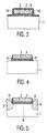
- Figs. 1 to 7 are diagrammatic cross-sectional views, not drawn to scale, of a semiconductor substrate during the various manufacturing steps according to the method according the invention.
- Fig. 1 shows a silicon substrate 1 on a surface of which a layer 2 of silicon oxynitride (SiO x N y ) extends on which a layer 3 of silicon nitride (Si 3 N 4 ) is provided.
- the layer 3 of silicon nitride may be provided, for example, while using conventionally used low-pressure vapor deposition techniques.
- the layer 2 of silicon oxynitride which is denoted by the chemical formula SiO x N y may be formed, for example, by simultaneous deposition of silicon nitride and silicon oxide. Such a layer may be considered as an oxygen-containing silicon nitride layer.
- the ratio x : y is smaller than 0.5, the protecting effect upon oxidizing the silicon substrate being comparable to that of a layer of silicon nitride of the same thickness.
- the thickness of the layer 3 of silicon nitride should be chosen to be so that the underlying surface of the substrate 1 is protected from undesired oxidation.
- a layer thickness of the order of magnitude of 50 to 200 nm is sufficient.
- the layer 2 of silicon oxynitride must be sufficiently thick to protect the substrate 1 from undesired mechanical stresses caused by the layer 3 of silicon nitride. In accordance with the invention a thickness of approximately 30 to 60 nm is sufficient for this purpose.
- a pattern 4 of photolacquer to form the mask is then provided on the layer 3 of silicon nitride in a manner known in practice, for example, by means of photolithographic techniques, by locally etching away the layer 3 of silicon nitride and the layer 2 of silicon oxynitride down to the substrate surface. Etching may be carried out, for example, in known manner with a fluorine-containing plasma. After the etching treatment the layer 4 of photolacquer is removed in a manner known in practice, so that, for example, the structure shown in Fig. 2 is obtained.
- a reduction of the lateral oxide growth can be produced by covering the edges of the apertures of the mask with the spacers already mentioned hereinbefore, before the first oxidation step is carried out for the formation according to the invention of the recesses in the substrate.
- the mask is covered with a further layer of silicon oxynitride, as is shown in Fig. 3 , which further layer is etched selectively by means of a fluorine-containing plasma in such a manner that the side walls 10 of the apertures of the mask remain covered with parts 11 (spacers) of the said further layer 9 of silicon oxynitride, as is shown in Fig. 4 .
- the dimensions of the spacers 11 near the substrate surface should be such that the undergrowth of the first oxide layer 5 to be formed again according to the invention is restricted to below the said spacers 11, as is shown in Fig. 5 .
- the thickness of the said further layer 9 of silicon oxynitride can be restricted according to the invention to approximately 40 to 60 nm.
- the exposed parts of the substrate surface are subjected according to the invention to a first oxidation treatment, for example, by heating the semiconductor wafer in a quartz tube to 900-1100 °C and leading a gas mixture consisting of hydrogen and an excess of oxygen over the semiconductor wafer.
- a gas mixture consisting of hydrogen and an excess of oxygen over the semiconductor wafer.
- a first oxide layer 5 is formed in a thickness of approximately 400 nm as is shown in Fig. 5 .
- the silicon oxide as a result of its specific volume which is approximately two times larger than the silicon, extends for substantially half its thickness in the substrate and for the other half above the substrate surface.
- the lateral growth of the said oxide layer in the active regions 8 of the substrate screened by the mask is restricted to approximately 50 nm, measured from the edge of the apertures of the mask, also while using the mask of silicon oxynitride and silicon nitride.
- the first oxide layer 5 thus formed is then subjected according to the invention to an isotropic etching treatment, preferably by means of a buffer solution of one part of hydrogen fluoride (HF) in seven parts of ammonium fluoride (NH 4 F).
- This buffer solution has such an etching selectivity that the silicon oxide is etched away approximately six times faster than the silicon oxynitride.
- a structure as shown in Fig. 6 is formed in which at the area of the oxide layer 5 an approximately 200 nm deep recess 6 is formed in the substrate.
- etching of silicon oxide is a process which can readily be controlled in practice, according to the invention recesses are formed which extend only over a distance of approximately 50 nm in the active regions of the substrate. Because as a result of the etching of the silicon oxide the silicon is substantially not attacked, the quality of the ultimately formed semiconductor device will be better than that of a semiconductor device obtained while using the known method in which etching is carried out with a solution of chromium.
- the dimensions of the spacers 11 will also decrease, for example, as is shown in Fig. 6 .
- the assembly is subjected to a second oxidation treatment by means of the said oxidizing gas mixture in which the partly sunken field oxide regions 7 are formed in a total thickness of approximately 400 nm, as is shown in Fig. 7 .
- the recesses 6 formed in the substrate 1 can readily be reached for the oxidizing gas mixture with which the sunken field oxide regions 7 are formed.
- the ultimately formed field oxide regions now show an undergrowth in the active regions 8 of less than 50 nm.
- the ultimately formed active regions 8 correspond to a sufficient extent to the dimensions of the mask, which enables the manufacture of a semiconductor device with comparatively small active regions, as is required for increasing the integration density.
- the thickness of the field oxide regions is determined by the required electric insulation between the active regions of the substrate. It will be obvious that in practice other layer thicknesses may also occur. In general, a 150 to 600 nm thick layer of silicon oxide will be provided in the first oxidation step and a 200 to 800 nm thick layer of silicon oxide will be provided with the oxidation step for the formation of the field oxide regions.
- the manufacture according to the invention of the spacers of silicon oxynitride has the advantage that the mechanical forces acting hereon are absorbed by the silicon oxynitride in such a manner that the spacers are not pushed away or are substantially not pushed away from the substrate surface.
- the mask of silicon oxynitride and silicon nitride mask as well as the remaining parts of the spacers 11 will in general be removed in a manner known in practice, after which the individual semiconductor elements, for example, transistors, diodes, etc., are formed in the active regions 8. Because in general several oxidation steps and etching steps are carried out the thickness of the formed field oxide regions 7 will generally decrease by another approximately 100 nm. In practice it is therefore advantageous to form field oxide regions which extend approximately 100 nm above the substrate surface. The field oxide projecting above the substrate surface will be removed at the end of the manufacturing steps so that sunken field oxide regions result having a substantially flat topography so that the electric wiring tracks for connection or interconnection of the individual semiconductor elements can relatively simply be provided.
- the first layer of silicon oxide is for this purpose formed in a thickness smaller than the thickness of the ultimate field oxide regions.
- a first oxide layer is formed in a thickness of approximately 300 nm. After etching this results in approximately 150 nm deep recesses in the silicon substrate determined by the mask.
- an approximately 500 nm thick oxide layer is then provided which extends over a distance of approximately 400 nm in the substrate and over approximately 100 nm above the substrate surface (not shown).
Landscapes
- Element Separation (AREA)
- Local Oxidation Of Silicon (AREA)
Description
Claims (2)
- A method of manufacturing a semiconductor device comprising a silicon substrate (1) with fully or partly sunken field oxide regions (7) for mutual insulation of semiconductor elements to be formed in the substrate (1), in which method a mask is formed in a layer of silicon oxynitride SiOxNy (2) deposited upon a surface of the substrate and an overlying layer of silicon nitride Si3N4 (3), whereby in the layer of silicon oxynitride (2) x/y is smaller than 0.5, after which, using said mask, recesses (6) are first provided in the substrate (1) in which recesses (6) the field oxide regions (7) are then formed by subjecting the recesses (6) over their whole area to an oxidation treatment, characterized in that the recesses (6) are provided in the substrate (1) by performing a first oxidation and then etching away the silicon oxide (5) thus formed, and in that prior to performing the first oxidation step a further layer of silicon oxynitride SiOxNy (9) is provided on the mask after which the said further layer of silicon oxynitride (9) is etched anisotropically in such a manner that the edges of the apertures of the mask (10) which bound the regions of the substrate (1) where the recesses (6) are provided remain covered with parts of the said further layer of silicon oxynitride (11).
- The method as claimed in Claim 1, characterized in that the further silicon oxynitride layer (9) is provided in a thickness of 40 to 60 nm.
Applications Claiming Priority (2)
| Application Number | Priority Date | Filing Date | Title |
|---|---|---|---|
| NL8800903A NL8800903A (en) | 1988-04-08 | 1988-04-08 | METHOD FOR MANUFACTURING A SEMICONDUCTOR DEVICE WITH A SILICONE SUBSTRATE WITH WHOLE OR PARTLY SUNCILLED FIELD OXIDE AREAS. |
| NL8800903 | 1988-04-08 |
Publications (2)
| Publication Number | Publication Date |
|---|---|
| EP0336515A1 EP0336515A1 (en) | 1989-10-11 |
| EP0336515B1 true EP0336515B1 (en) | 2001-10-17 |
Family
ID=19852091
Family Applications (1)
| Application Number | Title | Priority Date | Filing Date |
|---|---|---|---|
| EP89200845A Expired - Lifetime EP0336515B1 (en) | 1988-04-08 | 1989-04-03 | Method of manufacturing a semiconductor device having a silicon substrate with fully or partly sunken field oxide regions |
Country Status (5)
| Country | Link |
|---|---|
| EP (1) | EP0336515B1 (en) |
| JP (1) | JPH0212822A (en) |
| KR (1) | KR890016656A (en) |
| DE (1) | DE68929332T2 (en) |
| NL (1) | NL8800903A (en) |
Families Citing this family (3)
| Publication number | Priority date | Publication date | Assignee | Title |
|---|---|---|---|---|
| KR100197651B1 (en) * | 1995-11-03 | 1999-06-15 | 김영환 | Method of forming an element isolation film of semiconductor device |
| US5661072A (en) * | 1996-05-23 | 1997-08-26 | Micron Technology, Inc. | Method for reducing oxide thinning during the formation of a semiconductor device |
| JP6258672B2 (en) * | 2013-11-21 | 2018-01-10 | ルネサスエレクトロニクス株式会社 | Manufacturing method of semiconductor device |
Citations (2)
| Publication number | Priority date | Publication date | Assignee | Title |
|---|---|---|---|---|
| GB2083947A (en) * | 1980-09-15 | 1982-03-31 | Gen Electric | Method of making integrated circuits |
| EP0071203A2 (en) * | 1981-07-30 | 1983-02-09 | International Business Machines Corporation | Mask for thermal oxidation and method of forming dielectric isolation surrounding regions |
Family Cites Families (4)
| Publication number | Priority date | Publication date | Assignee | Title |
|---|---|---|---|---|
| US4038110A (en) * | 1974-06-17 | 1977-07-26 | Ibm Corporation | Planarization of integrated circuit surfaces through selective photoresist masking |
| NL8401711A (en) * | 1984-05-29 | 1985-12-16 | Philips Nv | METHOD FOR MANUFACTURING A SILICONE BODY SEMICONDUCTOR DEVICE INCLUDING A SUNCILLED OXIDE LAYER. |
| US4631219A (en) * | 1985-01-31 | 1986-12-23 | International Business Machines Corporation | Growth of bird's beak free semi-rox |
| NL8501720A (en) * | 1985-06-14 | 1987-01-02 | Philips Nv | METHOD FOR MANUFACTURING A SEMICONDUCTOR DEVICE IN WHICH A SILICONE PLATE IS LOCALLY PROVIDED WITH FIELD OXIDE WITH CHANNEL INTERRUPTER. |
-
1988
- 1988-04-08 NL NL8800903A patent/NL8800903A/en not_active Application Discontinuation
-
1989
- 1989-04-03 DE DE68929332T patent/DE68929332T2/en not_active Expired - Fee Related
- 1989-04-03 EP EP89200845A patent/EP0336515B1/en not_active Expired - Lifetime
- 1989-04-06 JP JP1085860A patent/JPH0212822A/en active Pending
- 1989-04-08 KR KR1019890004648A patent/KR890016656A/en not_active Ceased
Patent Citations (2)
| Publication number | Priority date | Publication date | Assignee | Title |
|---|---|---|---|---|
| GB2083947A (en) * | 1980-09-15 | 1982-03-31 | Gen Electric | Method of making integrated circuits |
| EP0071203A2 (en) * | 1981-07-30 | 1983-02-09 | International Business Machines Corporation | Mask for thermal oxidation and method of forming dielectric isolation surrounding regions |
Non-Patent Citations (1)
| Title |
|---|
| A E T KUIPER: "Hydrogenation during thermal nitridation of silicon dioxide", J. APPL PHYS, vol. 59, no. 8, 15 April 1986 (1986-04-15), pages 2765 - 2772 * |
Also Published As
| Publication number | Publication date |
|---|---|
| JPH0212822A (en) | 1990-01-17 |
| DE68929332D1 (en) | 2001-11-22 |
| DE68929332T2 (en) | 2002-07-04 |
| EP0336515A1 (en) | 1989-10-11 |
| KR890016656A (en) | 1989-11-29 |
| NL8800903A (en) | 1989-11-01 |
Similar Documents
| Publication | Publication Date | Title |
|---|---|---|
| US4333964A (en) | Method of making integrated circuits | |
| US5880004A (en) | Trench isolation process | |
| US4333965A (en) | Method of making integrated circuits | |
| US5149669A (en) | Method of forming an isolation region in a semiconductor device | |
| JPS6340337A (en) | Method of isolating integrated circuit | |
| JPH0864574A (en) | Silicon Nitride Etching Method | |
| US5019526A (en) | Method of manufacturing a semiconductor device having a plurality of elements | |
| EP0424011B1 (en) | Integrated-circuit device isolation | |
| US4612701A (en) | Method to reduce the height of the bird's head in oxide isolated processes | |
| US5397732A (en) | PBLOCOS with sandwiched thin silicon nitride layer | |
| EP0075875A2 (en) | Method of making integrated circuits comprising dielectric isolation regions | |
| US6867143B1 (en) | Method for etching a semiconductor substrate using germanium hard mask | |
| US6579766B1 (en) | Dual gate oxide process without critical resist and without N2 implant | |
| EP0336515A1 (en) | Method of manufacturing a semiconductor device having a silicon substrate with fully or partly sunken field oxide regions | |
| JP3178416B2 (en) | Method for manufacturing semiconductor device | |
| US5763316A (en) | Substrate isolation process to minimize junction leakage | |
| US6265286B1 (en) | Planarization of LOCOS through recessed reoxidation techniques | |
| KR0176193B1 (en) | Device Separation Method of Semiconductor Device | |
| US6194319B1 (en) | Semiconductor processing method of reducing an etch rate of one portion of a doped material relative to another portion, and methods of forming openings | |
| US6204547B1 (en) | Modified poly-buffered isolation | |
| US6245643B1 (en) | Method of removing polysilicon residual in a LOCOS isolation process using an etching selectivity solution | |
| JPS63205927A (en) | Manufacture of semiconductor device | |
| JP2586431B2 (en) | Method for manufacturing semiconductor device | |
| JPS59208744A (en) | Semiconductor device | |
| US6225682B1 (en) | Semiconductor memory device having isolation structure and method of fabricating the same |
Legal Events
| Date | Code | Title | Description |
|---|---|---|---|
| PUAI | Public reference made under article 153(3) epc to a published international application that has entered the european phase |
Free format text: ORIGINAL CODE: 0009012 |
|
| AK | Designated contracting states |
Kind code of ref document: A1 Designated state(s): DE FR GB IT NL |
|
| 17P | Request for examination filed |
Effective date: 19900406 |
|
| 17Q | First examination report despatched |
Effective date: 19921001 |
|
| RAP3 | Party data changed (applicant data changed or rights of an application transferred) |
Owner name: KONINKLIJKE PHILIPS ELECTRONICS N.V. |
|
| APAD | Appeal reference recorded |
Free format text: ORIGINAL CODE: EPIDOS REFNE |
|
| APAB | Appeal dossier modified |
Free format text: ORIGINAL CODE: EPIDOS NOAPE |
|
| GRAG | Despatch of communication of intention to grant |
Free format text: ORIGINAL CODE: EPIDOS AGRA |
|
| RIC1 | Information provided on ipc code assigned before grant |
Free format text: 7H 01L 21/762 A, 7H 01L 21/32 B |
|
| GRAG | Despatch of communication of intention to grant |
Free format text: ORIGINAL CODE: EPIDOS AGRA |
|
| GRAH | Despatch of communication of intention to grant a patent |
Free format text: ORIGINAL CODE: EPIDOS IGRA |
|
| GRAH | Despatch of communication of intention to grant a patent |
Free format text: ORIGINAL CODE: EPIDOS IGRA |
|
| GRAA | (expected) grant |
Free format text: ORIGINAL CODE: 0009210 |
|
| AK | Designated contracting states |
Kind code of ref document: B1 Designated state(s): DE FR GB IT NL |
|
| PG25 | Lapsed in a contracting state [announced via postgrant information from national office to epo] |
Ref country code: IT Free format text: LAPSE BECAUSE OF FAILURE TO SUBMIT A TRANSLATION OF THE DESCRIPTION OR TO PAY THE FEE WITHIN THE PRE;WARNING: LAPSES OF ITALIAN PATENTS WITH EFFECTIVE DATE BEFORE 2007 MAY HAVE OCCURRED AT ANY TIME BEFORE 2007. THE CORRECT EFFECTIVE DATE MAY BE DIFFERENT FROM THE ONE RECORDED.SCRIBED TIME-LIMIT Effective date: 20011017 Ref country code: NL Free format text: LAPSE BECAUSE OF FAILURE TO SUBMIT A TRANSLATION OF THE DESCRIPTION OR TO PAY THE FEE WITHIN THE PRESCRIBED TIME-LIMIT Effective date: 20011017 |
|
| REF | Corresponds to: |
Ref document number: 68929332 Country of ref document: DE Date of ref document: 20011122 |
|
| REG | Reference to a national code |
Ref country code: GB Ref legal event code: IF02 |
|
| ET | Fr: translation filed | ||
| NLV1 | Nl: lapsed or annulled due to failure to fulfill the requirements of art. 29p and 29m of the patents act | ||
| PGFP | Annual fee paid to national office [announced via postgrant information from national office to epo] |
Ref country code: FR Payment date: 20020426 Year of fee payment: 14 |
|
| PGFP | Annual fee paid to national office [announced via postgrant information from national office to epo] |
Ref country code: GB Payment date: 20020430 Year of fee payment: 14 |
|
| PGFP | Annual fee paid to national office [announced via postgrant information from national office to epo] |
Ref country code: DE Payment date: 20020625 Year of fee payment: 14 |
|
| PLBE | No opposition filed within time limit |
Free format text: ORIGINAL CODE: 0009261 |
|
| STAA | Information on the status of an ep patent application or granted ep patent |
Free format text: STATUS: NO OPPOSITION FILED WITHIN TIME LIMIT |
|
| 26N | No opposition filed | ||
| REG | Reference to a national code |
Ref country code: GB Ref legal event code: 746 Effective date: 20021025 |
|
| REG | Reference to a national code |
Ref country code: FR Ref legal event code: D6 |
|
| PG25 | Lapsed in a contracting state [announced via postgrant information from national office to epo] |
Ref country code: GB Free format text: LAPSE BECAUSE OF NON-PAYMENT OF DUE FEES Effective date: 20030403 |
|
| PG25 | Lapsed in a contracting state [announced via postgrant information from national office to epo] |
Ref country code: DE Free format text: LAPSE BECAUSE OF NON-PAYMENT OF DUE FEES Effective date: 20031101 |
|
| GBPC | Gb: european patent ceased through non-payment of renewal fee |
Effective date: 20030403 |
|
| PG25 | Lapsed in a contracting state [announced via postgrant information from national office to epo] |
Ref country code: FR Free format text: LAPSE BECAUSE OF NON-PAYMENT OF DUE FEES Effective date: 20031231 |
|
| REG | Reference to a national code |
Ref country code: FR Ref legal event code: ST |
|
| APAH | Appeal reference modified |
Free format text: ORIGINAL CODE: EPIDOSCREFNO |