EP0335509B1 - Broad band VCO control system for clock recovery - Google Patents
Broad band VCO control system for clock recovery Download PDFInfo
- Publication number
- EP0335509B1 EP0335509B1 EP89302093A EP89302093A EP0335509B1 EP 0335509 B1 EP0335509 B1 EP 0335509B1 EP 89302093 A EP89302093 A EP 89302093A EP 89302093 A EP89302093 A EP 89302093A EP 0335509 B1 EP0335509 B1 EP 0335509B1
- Authority
- EP
- European Patent Office
- Prior art keywords
- signal
- clock
- circuit
- counter
- phase
- Prior art date
- Legal status (The legal status is an assumption and is not a legal conclusion. Google has not performed a legal analysis and makes no representation as to the accuracy of the status listed.)
- Expired - Lifetime
Links
Images

Classifications
-
- H—ELECTRICITY
- H04—ELECTRIC COMMUNICATION TECHNIQUE
- H04L—TRANSMISSION OF DIGITAL INFORMATION, e.g. TELEGRAPHIC COMMUNICATION
- H04L7/00—Arrangements for synchronising receiver with transmitter
- H04L7/02—Speed or phase control by the received code signals, the signals containing no special synchronisation information
- H04L7/033—Speed or phase control by the received code signals, the signals containing no special synchronisation information using the transitions of the received signal to control the phase of the synchronising-signal-generating means, e.g. using a phase-locked loop
-
- Y—GENERAL TAGGING OF NEW TECHNOLOGICAL DEVELOPMENTS; GENERAL TAGGING OF CROSS-SECTIONAL TECHNOLOGIES SPANNING OVER SEVERAL SECTIONS OF THE IPC; TECHNICAL SUBJECTS COVERED BY FORMER USPC CROSS-REFERENCE ART COLLECTIONS [XRACs] AND DIGESTS
- Y10—TECHNICAL SUBJECTS COVERED BY FORMER USPC
- Y10S—TECHNICAL SUBJECTS COVERED BY FORMER USPC CROSS-REFERENCE ART COLLECTIONS [XRACs] AND DIGESTS
- Y10S331/00—Oscillators
- Y10S331/02—Phase locked loop having lock indicating or detecting means
Definitions
- This invention relates to a clock circuit including a controlled oscillator for use in providing a clock signal locked in phase to an incoming data signal.
- Data signals are increasingly transmitted along fibre optic links.
- Such data signals normally have a well defined frequency, for example 125 Mbs ⁇ 1, but have a significant amount of phase jitter, caused by signal dispersion within the optical fibres, differential slew rates of the date edge transitions caused by diode switching, and noise in transimpedance amplifiers.
- FDDI frequency division duplex interleaved data
- a set rate typically 125 Mbs ⁇ 1 in 4B/5B format (a five bit code word representing four data bits) and in non-return to zero inverse (NRZ1) coding wherein in any bit period a positive or negative voltage transition indicates a '1' bit and the absence of a transition indicates a '0' bit.
- transitions may occur at a maximum rate of once every bit period and at a minimum rate of once every ten bit periods (known as the master line state).
- a major problem in the design of receiver circuits is that of phase jitter in the incoming data signal, requiring a local receiver clock having a well defined operating frequency together with a control circuit which accurately locks the oscillator to the incoming data signal and can rapidly adjust to phase deviations, and furthermore lends itself to integration.
- Oscillators with a well defined operating frequency are commonly of the L-C type with components such as varicap diodes which cannot be formed on an integrated circuit.
- the present invention provides a clock circuit for providing a clock signal locked in phase to an incoming data signal which includes transitions between upper and lower voltage levels, the clock circuit including a phase locked loop having a controlled oscillator providing said clock signal, a phase detector circuit responsive to said clock signal and to the incoming data signal for providing a first phase error signal, a reference clock source, and means for comparing the reference clock signal with said clock signal to provide a second phase error signal, characterised in that the clock circuit includes mode selection means for selecting either the first or second phase error signal for control of the controlled oscillator, said mode selection means including first and second counters (28, 26) for counting predetermined numbers of cycles of the reference clock source and the controlled oscillator (14), respectively, the first counter (28) providing a control signal upon reaching a predetermined count of the reference clock source to the second counter (26) which thereupon stops counting, the second counter (26) including control output means for providing signals indicating whether the count thereof is within predetermined tolerance bands, for control of the mode selection means (24, 16).
- said means for comparing comprises a phase frequency comparator which ensures a frequency lock prior to providing phase error information, and said selection means is a multiplexer.
- the controlled oscillator may be a voltage controlled oscillator (VCO) of any suitable type which relies upon a capacitive charging arrangement, for example a multivibrator, to define the oscillation frequency, in order that the oscillator be fabricated as an integrated circuit.
- VCO voltage controlled oscillator
- the VCO Since the incoming data signal will normally have a well defined frequency, the VCO is firstly set up locked in frequency to the reference clock by means of a phase frequency comparator, the frequency of the VCO thus being held within tightly defined limits.
- a counter is provided which counts a predetermined number, for example 200, of cycles of the VCO over a predetermined period, say 40 cycles, of the reference clock. A tolerance of ⁇ 1 count is permitted to allow for a miscount due to edge jitter noise of the reference frequency source.
- the selection means selects the phase detector circuit in a second stage of operation, so that the first error signal provided by the phase detector circuit is applied to the VCO. Since a significant amount of phase jitter will normally be present, a similar method of checking phase lock may be employed by counting 200 cycles of the VCO over 40 cycles of the reference clock, but a larger count tolerance is permitted, say ⁇ 3 counts.
- a receiver for receiving incoming data RCVD being data transmitted across an optical fibre link at 125 Mbs ⁇ 1 in an NRZ1 code wherein a '1' bit is indicated by a voltage level transition (positive or negative) in a bit period and a 'O' bit is indicated by the absence of a transition.
- Data signal RCVD is applied to a phase detector 10 and to a data converter 12, which circuits also receive a local clock signal CK from a VCO 14.
- Detector 10 is operative to compare the phase of the incoming data with the phase of the clock signal in order to provide a phase error signal to VCO 14, via a linear multiplexer 16 and a charge pump and filter 18.
- Converter 12 gates the incoming data signal with clock CK in order to provide a Data Received signal in suitable form e.g. NRZ.
- the phase error signal from comparator 20 is applied to VCO 14 via linear multiplexer 16.
- Linear multiplexer 16 is operative to select the inputs from detector 10 and comparator 20 under the control of mode select logic 24.
- Logic 24 operates under the control of eight bit counter 26 which counts 200 cycles of CK signal in a period determined by ⁇ 43 counter 28 as 40 cycles of LSCK signal.
- FIG. 3 A detailed diagram of counter 28 is shown in Figure 3, as comprising D-type flip flops D1 to D8.
- Signal LSCK is applied to the clock inputs of D1 to D3, and a reset input RES from logic 24 is applied to the D inputs of D1, D2 via AND gates AN1, AN2.
- OR gates OR2 to 4, NOR gate NO1 and AND gate AN3 complete the counter.
- the counter provides a ⁇ 43 facility of the incoming LSCK signal (25 MHz) in two stages, firstly a ⁇ 40 function which is signalled by output C1, which is provided to divider circuit 26, and secondly, within the three extra division steps, an output OP2 which provides a control signal to select logic 24 and an output OP3 which provides a reset signal both to the ⁇ 43 counter and to counter 26.
- a detailed diagram of counts 26 is shown in Figure 2 as comprising a chain of D-type flip-flops D1 to D9, OR gates OR2 to 5, NOR gates NO1 to NO3 and two multiplexers MUX2W and ORMUX.
- Flip-flop D1 receives a clock signal CK from VCO 14.
- a reset signal LD is provided from OP3 of counter 28 and a C1 control signal is applied to MUX2W from OP1 of counter 28.
- Counter 26 provides outputs FCN and FCW to mode select logic 24.
- Output FCW indicates, when high, a nominal count of 200 which is within limits of ⁇ 3 whereas output FCN indicates, when high, a nominal count of 200 which is within limits of ⁇ 1.
- mode select logic 24 is shown in Figure 4 as comprising two D-type flip-flop D1, D2, AND gates AN1 to AN3 and multiplexers MUX2W and ORMUX.
- Clock signal LSCK clocks flip-flops D1 and D2.
- Input signal RD from output OP2 of counter 28 is operative to enable input FCN and input FCW from counter 26.
- FCW may provide a mode change whereby MODE output provides a signal to linear mulitplexer 16 in order to change the mode of operation of the circuit.
- a RES output is provided to circuit 28 in order to reset the counter.
- the circuit is initially set up with multiplexer 16 selecting the output from phase frequency comparator 20 for application to VCO 14.
- reference signal LSCK is compared with signal CK from VCO 14 (divided by N in circuit 22).
- the output from comparator 20 represents the phase difference between signals CK and LSCK when the frequencies are identical.
- counter 26 is operative to count 200 cycles of CK.
- flip-flop D2 of counter 28 provides a high signal at OP3 which acts as signal LD to clear flip-flops D1 to D9 of counter 28.
- OP3 acts as signal LD to clear flip-flops D1 to D9 of counter 28.
- counter 26 commences to count cycles of CK while counter 28 counts cycles of signal LSCK.
- counter 28 After 40 cycles of LSCK as determined by counter 28, counter 28 provides a signal OP1 as signal C1 to multiplexer MUX2W of counter 26 and a signal OP2 as signal RD to the multiplexers of mode select logic 24.
- These signals serve to enable outputs FCN and FCW of counter 26 and enable mode select logic 24 to respond to outputs FCN and FCW.
- counter 26 will count nominally 200 cycles of CK. Since VCO 14 is tracking signal LSCK, the count of counter 26 should be very close to 200. Since there may be some amount of edge jitter, a tolerance of ⁇ 1 is permitted in the count; if the count of counter 200 falls outside this tolerance band then signal FCW goes high, this signal causing mode select logic to provide RES signal to reset counter 28 in order that the counters restart.
- the circuit remains in this mode of operation until a count of 200 is achieved within the tolerance band of ⁇ 1 at which time mode select logic 24 will provide a MODE signal in order that multiplexer 16 select the phase error output signal from phase detector 10, so that VCO 14 tracks the clock rate of data signal RCVD.
- data signal RCVD is received in a converter 12 which is clocked by signal CK.
- the clock rate of VCO 14 is again checked and at the end of 40 cycles of LSCK as determined by counter 28, the contents of counter 26 are assessed. If the output of FCW is high this indicates the count is outside the tolerance band of ⁇ 3 and the circuit is assumed to have lost synchronisation with data signal RCVD.
- signal FCW causes mode select logic 24 to change the mode of operation so that VCO is reinitialised to reference clock signal LSCK. If however signal FCW indicates that the tolerance band of ⁇ 3 has not been exceeded, then the circuits remains in the receive data condition in which VCO 14 is locked to the incoming data signal RCVD.
Landscapes
- Engineering & Computer Science (AREA)
- Computer Networks & Wireless Communication (AREA)
- Signal Processing (AREA)
- Stabilization Of Oscillater, Synchronisation, Frequency Synthesizers (AREA)
Description
- This invention relates to a clock circuit including a controlled oscillator for use in providing a clock signal locked in phase to an incoming data signal.
- Data signals are increasingly transmitted along fibre optic links. Such data signals normally have a well defined frequency, for example 125 Mbs⁻¹, but have a significant amount of phase jitter, caused by signal dispersion within the optical fibres, differential slew rates of the date edge transitions caused by diode switching, and noise in transimpedance amplifiers.
- An international standard, FDDI, has been set requiring that data be transmitted at a set rate, typically 125 Mbs⁻¹ in 4B/5B format (a five bit code word representing four data bits) and in non-return to zero inverse (NRZ1) coding wherein in any bit period a positive or negative voltage transition indicates a '1' bit and the absence of a transition indicates a '0' bit. Thus transitions may occur at a maximum rate of once every bit period and at a minimum rate of once every ten bit periods (known as the master line state).
- A major problem in the design of receiver circuits is that of phase jitter in the incoming data signal, requiring a local receiver clock having a well defined operating frequency together with a control circuit which accurately locks the oscillator to the incoming data signal and can rapidly adjust to phase deviations, and furthermore lends itself to integration.
- Oscillators with a well defined operating frequency are commonly of the L-C type with components such as varicap diodes which cannot be formed on an integrated circuit.
- In the publication Data Communications, Volume 15, No. 2, February 1986, pages 143 and 144, there is disclosed a clock recovery circuit having two phase detectors, one of which is used during normal data transmission and the other of which is used before transmission or during error conditions to synchronize to a local crystal-controlled oscillator, making it possible to have both a large loop bandwidth and a small initial frequency error.
- The present invention provides a clock circuit for providing a clock signal locked in phase to an incoming data signal which includes transitions between upper and lower voltage levels, the clock circuit including a phase locked loop having a controlled oscillator providing said clock signal, a phase detector circuit responsive to said clock signal and to the incoming data signal for providing a first phase error signal, a reference clock source, and means for comparing the reference clock signal with said clock signal to provide a second phase error signal, characterised in that the clock circuit includes mode selection means for selecting either the first or second phase error signal for control of the controlled oscillator, said mode selection means including first and second counters (28, 26) for counting predetermined numbers of cycles of the reference clock source and the controlled oscillator (14), respectively, the first counter (28) providing a control signal upon reaching a predetermined count of the reference clock source to the second counter (26) which thereupon stops counting, the second counter (26) including control output means for providing signals indicating whether the count thereof is within predetermined tolerance bands, for control of the mode selection means (24, 16).
- Preferably said means for comparing comprises a phase frequency comparator which ensures a frequency lock prior to providing phase error information, and said selection means is a multiplexer.
- The controlled oscillator may be a voltage controlled oscillator (VCO) of any suitable type which relies upon a capacitive charging arrangement, for example a multivibrator, to define the oscillation frequency, in order that the oscillator be fabricated as an integrated circuit. With oscillators such as multivibrators it is a simple measure to adjust the frequency by adjusting the capacitive charging rate.
- Since the incoming data signal will normally have a well defined frequency, the VCO is firstly set up locked in frequency to the reference clock by means of a phase frequency comparator, the frequency of the VCO thus being held within tightly defined limits. As preferred, a counter is provided which counts a predetermined number, for example 200, of cycles of the VCO over a predetermined period, say 40 cycles, of the reference clock. A tolerance of ±1 count is permitted to allow for a miscount due to edge jitter noise of the reference frequency source. When the frequency of the oscillator is determined to be locked to the reference clock, and the phase of the oscillator remains in phase with that of the reference clock, then the selection means selects the phase detector circuit in a second stage of operation, so that the first error signal provided by the phase detector circuit is applied to the VCO. Since a significant amount of phase jitter will normally be present, a similar method of checking phase lock may be employed by counting 200 cycles of the VCO over 40 cycles of the reference clock, but a larger count tolerance is permitted, say ±3 counts.
- If the incoming data signal goes out of limits as checked by the counter, the data signal is assumed invalid and the clock circuit reverts to locking the VCO to the reference clock signal.
- A preferred embodiment of the invention will now be described with reference to the accompanying drawings, wherein:-
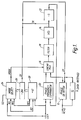
- Figure 1 is a block diagram of the preferred embodiment; and,
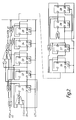
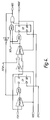
- Figures 2, 3 and 4 are detailed block diagrams of counter circuits and mode select logic employed in Figure 1.
- Referring now to Figure 1, there is shown a receiver for receiving incoming data RCVD, being data transmitted across an optical fibre link at 125 Mbs⁻¹ in an NRZ1 code wherein a '1' bit is indicated by a voltage level transition (positive or negative) in a bit period and a 'O' bit is indicated by the absence of a transition.
- Data signal RCVD is applied to a
phase detector 10 and to adata converter 12, which circuits also receive a local clock signal CK from a VCO 14.Detector 10 is operative to compare the phase of the incoming data with the phase of the clock signal in order to provide a phase error signal to VCO 14, via a linear multiplexer 16 and a charge pump andfilter 18. Converter 12 gates the incoming data signal with clock CK in order to provide a Data Received signal in suitable form e.g. NRZ. - A reference clock signal LSCK of a frequency of e.g. 25 MHz, is applied to a
phase frequency comparator 20 together with a version of clock signal CK divided down to the reference frequency by a divider ÷ 5 (more generally ÷N) 22. The phase error signal fromcomparator 20 is applied to VCO 14 via linear multiplexer 16. Linear multiplexer 16 is operative to select the inputs fromdetector 10 andcomparator 20 under the control of modeselect logic 24.Logic 24 operates under the control of eightbit counter 26 which counts 200 cycles of CK signal in a period determined by ÷43counter 28 as 40 cycles of LSCK signal. - A detailed diagram of
counter 28 is shown in Figure 3, as comprising D-type flip flops D1 to D8. Signal LSCK is applied to the clock inputs of D1 to D3, and a reset input RES fromlogic 24 is applied to the D inputs of D1, D2 via AND gates AN1, AN2. OR gates OR2 to 4, NOR gate NO1 and AND gate AN3 complete the counter. The counter provides a ÷43 facility of the incoming LSCK signal (25 MHz) in two stages, firstly a ÷40 function which is signalled by output C1, which is provided todivider circuit 26, and secondly, within the three extra division steps, an output OP2 which provides a control signal to selectlogic 24 and an output OP3 which provides a reset signal both to the ÷43 counter and to counter 26. - A detailed diagram of
counts 26 is shown in Figure 2 as comprising a chain of D-type flip-flops D1 to D9, OR gates OR2 to 5, NOR gates NO1 to NO3 and two multiplexers MUX2W and ORMUX. Flip-flop D1 receives a clock signal CK from VCO 14. A reset signal LD is provided from OP3 ofcounter 28 and a C1 control signal is applied to MUX2W from OP1 ofcounter 28. Counter 26 provides outputs FCN and FCW to modeselect logic 24. Output FCW indicates, when high, a nominal count of 200 which is within limits of ±3 whereas output FCN indicates, when high, a nominal count of 200 which is within limits of ±1. - A detailed diagram of mode
select logic 24 is shown in Figure 4 as comprising two D-type flip-flop D1, D2, AND gates AN1 to AN3 and multiplexers MUX2W and ORMUX. Clock signal LSCK clocks flip-flops D1 and D2. Input signal RD from output OP2 ofcounter 28 is operative to enable input FCN and input FCW fromcounter 26. When selected, either input FCN, FCW may provide a mode change whereby MODE output provides a signal to linear mulitplexer 16 in order to change the mode of operation of the circuit. In addition a RES output is provided tocircuit 28 in order to reset the counter. - A detailed description of the circuits of Figures 2,3 and 4 will not be given, since their precise manner of operation will be apparent to one skilled in the art.
- In operation, the circuit is initially set up with multiplexer 16 selecting the output from
phase frequency comparator 20 for application to VCO 14. Thus in this mode of operation reference signal LSCK is compared with signal CK from VCO 14 (divided by N in circuit 22). - The output from
comparator 20 represents the phase difference between signals CK and LSCK when the frequencies are identical. In order to check that the frequency of the VCO is correct,counter 26 is operative to count 200 cycles of CK. Thus whencounter 28 is reset by signal RES, flip-flop D2 ofcounter 28 provides a high signal at OP3 which acts as signal LD to clear flip-flops D1 to D9 ofcounter 28. Thus at thistime counter 26 commences to count cycles of CK while counter 28 counts cycles of signal LSCK. After 40 cycles of LSCK as determined bycounter 28,counter 28 provides a signal OP1 as signal C1 to multiplexer MUX2W ofcounter 26 and a signal OP2 as signal RD to the multiplexers of modeselect logic 24. These signals serve to enable outputs FCN and FCW ofcounter 26 and enable modeselect logic 24 to respond to outputs FCN and FCW. - Thus at the end of 40 cycles of LSCK as determined by
counter 28,counter 26 will count nominally 200 cycles of CK. Since VCO 14 is tracking signal LSCK, the count ofcounter 26 should be very close to 200. Since there may be some amount of edge jitter, a tolerance of ±1 is permitted in the count; if the count of counter 200 falls outside this tolerance band then signal FCW goes high, this signal causing mode select logic to provide RES signal to resetcounter 28 in order that the counters restart. - Thus the circuit remains in this mode of operation until a count of 200 is achieved within the tolerance band of ±1 at which time mode
select logic 24 will provide a MODE signal in order that multiplexer 16 select the phase error output signal fromphase detector 10, so that VCO 14 tracks the clock rate of data signal RCVD. In this mode of operation data signal RCVD is received in aconverter 12 which is clocked by signal CK. The clock rate of VCO 14 is again checked and at the end of 40 cycles of LSCK as determined bycounter 28, the contents ofcounter 26 are assessed. If the output of FCW is high this indicates the count is outside the tolerance band of ±3 and the circuit is assumed to have lost synchronisation with data signal RCVD. In this case, signal FCW causes modeselect logic 24 to change the mode of operation so that VCO is reinitialised to reference clock signal LSCK. If however signal FCW indicates that the tolerance band of ±3 has not been exceeded, then the circuits remains in the receive data condition in which VCO 14 is locked to the incoming data signal RCVD. - There has thus been shown and described a highly accurate circuit for determining with precision an incoming data signal. The circuit relies on VLSI techniques in that counters 36 and 38 have a large transistor count and it is only with VLSI techniques that such counters may be incorporated into an IC chip with the remainder of the detector circuit.
Claims (7)
- A clock circuit for providing a clock signal locked in phase to an incoming data signal which includes transitions between upper and lower voltage levels, the clock circuit including a phase locked loop having a controlled oscillator (14) providing said clock signal, a phase detector circuit (10) responsive to said clock signal and to the incoming data signal for providing a first phase error signal, a reference clock source, and means (20) for comparing the reference clock signal with said clock signal to provide a second phase error signal, characterised in that the clock circuit includes mode selection means (24, 16) for selecting either the first or second phase error signal for control of the controlled oscillator (14), said mode selection means including first and second counters (28, 26) for counting predetermined numbers of cycles of the reference clock source and the controlled oscillator (14), respectively, the first counter (28) providing a control signal upon reaching a predetermined count of the reference clock source to the second counter (26) which thereupon stops counting, the second counter (26) including control output means for providing signals indicating whether the count thereof is within predetermined tolerance bands, for control of the mode selection means (24, 16).
- A clock circuit as claimed in Claim 1 wherein the controlled oscillator is a voltage controlled oscillator.
- A clock circuit as claimed in Claim 1 or 2 wherein the clock circuit forms part of a data receiver circuit for NRZI data wherein in any bit period the absence of a voltage transition indicates a 'O' bit and the presence of a transition indicates a '1' bit.
- A clock circuit as claimed in any preceding claim wherein said means (20) for comparing the reference clock signal with said clock signal comprises a phase frequency comparator.
- A clock circuit as claimed in any preceding claim wherein said mode selection means (24, 16) comprises a multiplexer (16) to which the first and second phase error signals are applied as inputs, the output being applied to the controlled oscillator (14).
- A clock circuit as claimed in Claim 1 wherein when the circuit is in a mode in which the controlled oscillator (14) responds to said second error signal, said control output means provides a signal indicating whether the count of the second counter (26) is within a first predetermined tolerance band, and if so, said mode selection means (24, 16) is operable to select the first phase error signal.
- A clock circuit as claimed in Claim 6 wherein when the circuit is in the mode in which the first phase error is selected, said control output means provides a signal indicating whether the count of the second counter (26) is within a second predetermined tolerance band, and if not, said mode selection means (24, 16) is operable to select the second phase error signal.
Applications Claiming Priority (2)
| Application Number | Priority Date | Filing Date | Title |
|---|---|---|---|
| GB8807320 | 1988-03-28 | ||
| GB8807320A GB2223136B (en) | 1988-03-28 | 1988-03-28 | Broad band vco control system for clock recovery |
Publications (3)
| Publication Number | Publication Date |
|---|---|
| EP0335509A2 EP0335509A2 (en) | 1989-10-04 |
| EP0335509A3 EP0335509A3 (en) | 1991-02-06 |
| EP0335509B1 true EP0335509B1 (en) | 1995-09-06 |
Family
ID=10634221
Family Applications (1)
| Application Number | Title | Priority Date | Filing Date |
|---|---|---|---|
| EP89302093A Expired - Lifetime EP0335509B1 (en) | 1988-03-28 | 1989-03-02 | Broad band VCO control system for clock recovery |
Country Status (5)
| Country | Link |
|---|---|
| US (1) | US4943788A (en) |
| EP (1) | EP0335509B1 (en) |
| JP (1) | JPH0263218A (en) |
| DE (1) | DE68924086T2 (en) |
| GB (1) | GB2223136B (en) |
Families Citing this family (35)
| Publication number | Priority date | Publication date | Assignee | Title |
|---|---|---|---|---|
| JPH02124637A (en) * | 1988-11-02 | 1990-05-11 | Nec Corp | Synchronization detection circuit |
| KR910009808B1 (en) * | 1989-06-13 | 1991-11-30 | 한국전기통신공사 | Digital automatic phase control retiming circuit |
| JP2938562B2 (en) * | 1990-11-28 | 1999-08-23 | 株式会社日立製作所 | Phase locked loop IC |
| US5319680A (en) * | 1991-09-03 | 1994-06-07 | The Whitaker Corporation | Phase locked loop synchronization system for use in data communications |
| WO1993025023A1 (en) * | 1992-06-02 | 1993-12-09 | Telefonaktiebolaget Lm Ericsson | Clock extraction circuit for fiber optical receivers |
| US5473639A (en) * | 1993-07-26 | 1995-12-05 | Hewlett-Packard Company | Clock recovery apparatus with means for sensing an out of lock condition |
| JP3033654B2 (en) * | 1993-08-23 | 2000-04-17 | 日本電気株式会社 | PLL frequency synthesizer |
| FR2713034B1 (en) * | 1993-11-23 | 1996-01-26 | Matra Mhs | Clock recovery circuit with paired oscillators. |
| US5579348A (en) * | 1994-02-02 | 1996-11-26 | Gi Corporation | Method and apparatus for improving the apparent accuracy of a data receiver clock circuit |
| US5512860A (en) * | 1994-12-02 | 1996-04-30 | Pmc-Sierra, Inc. | Clock recovery phase locked loop control using clock difference detection and forced low frequency startup |
| WO1997007594A1 (en) * | 1995-08-14 | 1997-02-27 | Hitachi, Ltd. | Pll circuit and picture reproducing device |
| US6388753B1 (en) | 1996-03-14 | 2002-05-14 | Massachusetts Institute Of Technology | All-optical bit phase sensing and clock recovery apparatus and methods |
| US5745011A (en) * | 1996-06-05 | 1998-04-28 | Cypress Semiconductor Corporation | Data recovery phase locked loop |
| US6285722B1 (en) | 1997-12-05 | 2001-09-04 | Telcordia Technologies, Inc. | Method and apparatus for variable bit rate clock recovery |
| US6341355B1 (en) | 1999-03-16 | 2002-01-22 | Lsi Logic Corporation | Automatic clock switcher |
| RU2153230C1 (en) * | 1999-03-24 | 2000-07-20 | Научно-исследовательский институт "Вектор" | Method and device for synchronization of complex m sequence |
| US6177843B1 (en) * | 1999-05-26 | 2001-01-23 | Cypress Semiconductor Corp. | Oscillator circuit controlled by programmable logic |
| US6526113B1 (en) * | 1999-08-11 | 2003-02-25 | Broadcom Corporation | GM cell based control loops |
| US6366135B1 (en) | 1999-12-23 | 2002-04-02 | Cypress Semiconductor Corp. | Data frequency detector |
| US6683930B1 (en) | 1999-12-23 | 2004-01-27 | Cypress Semiconductor Corp. | Digital phase/frequency detector, and clock generator and data recovery PLL containing the same |
| US6310521B1 (en) * | 1999-12-23 | 2001-10-30 | Cypress Semiconductor Corp. | Reference-free clock generation and data recovery PLL |
| RU2244384C2 (en) * | 2002-01-21 | 2005-01-10 | Новочеркасский военный институт связи | Method and device for timing m-sequence |
| US7720113B2 (en) * | 2004-04-23 | 2010-05-18 | Panasonic Corporation | Receiving apparatus, receiving system using same, and receiving method thereof |
| US20060247906A1 (en) * | 2005-04-27 | 2006-11-02 | International Business Machines Corporation | Method for estimating clock jitter for static timing measurements of modeled circuits |
| RU2320080C2 (en) * | 2005-09-07 | 2008-03-20 | Новочеркасское Высшее Военное Командное Училище Связи (Институт Связи) | Method and device for synchronization of pseudo-random sequences |
| US7920665B1 (en) | 2005-09-28 | 2011-04-05 | Cypress Semiconductor Corporation | Symmetrical range controller circuit and method |
| US7288975B2 (en) * | 2005-10-27 | 2007-10-30 | International Business Machines Corporation | Method and apparatus for fail-safe and restartable system clock generation |
| US8035455B1 (en) | 2005-12-21 | 2011-10-11 | Cypress Semiconductor Corporation | Oscillator amplitude control network |
| US7728675B1 (en) | 2006-03-31 | 2010-06-01 | Cypress Semiconductor Corporation | Fast lock circuit for a phase lock loop |
| US8120430B1 (en) | 2009-01-15 | 2012-02-21 | Xilinx, Inc. | Stable VCO operation in absence of clock signal |
| US8111106B2 (en) * | 2010-03-02 | 2012-02-07 | Cisco Technology, Inc. | Switched phase and frequency detector based DPLL circuit with excellent wander and jitter performance and fast frequency acquisition |
| US9237004B2 (en) * | 2013-09-16 | 2016-01-12 | Himax Technologies Limited | Clock data recovery circuit |
| TWI559723B (en) * | 2014-08-11 | 2016-11-21 | 聯詠科技股份有限公司 | Clock and data recovery apparatus |
| WO2016119139A1 (en) * | 2015-01-28 | 2016-08-04 | Texas Instruments Incorporated | Fault detection and self-recovery method for crystal oscillator |
| WO2023027078A1 (en) * | 2021-08-25 | 2023-03-02 | ヌヴォトンテクノロジージャパン株式会社 | Pll circuit and transmission system |
Family Cites Families (8)
| Publication number | Priority date | Publication date | Assignee | Title |
|---|---|---|---|---|
| US4069462A (en) * | 1976-12-13 | 1978-01-17 | Data General Corporation | Phase-locked loops |
| US4191976A (en) * | 1978-09-26 | 1980-03-04 | Data General Corporation | Circuit indicating phase relationship |
| US4222009A (en) * | 1978-11-02 | 1980-09-09 | Sperry Corporation | Phase lock loop preconditioning circuit |
| US4404530A (en) * | 1980-10-22 | 1983-09-13 | Data General Corporation | Phase locked loop with compensation for loop phase errors |
| US4365211A (en) * | 1980-10-31 | 1982-12-21 | Westinghouse Electric Corp. | Phase-locked loop with initialization loop |
| EP0060307B1 (en) * | 1981-03-12 | 1985-07-17 | International Business Machines Corporation | Method for connecting or disconnecting selected stations in a ring communication system, and ring communication system including selectively connectable stations |
| GB2187316B (en) * | 1986-02-28 | 1989-11-29 | Plessey Co Plc | Improvements in or relating to integrate circuits. |
| US4787097A (en) * | 1987-02-11 | 1988-11-22 | International Business Machines Corporation | NRZ phase-locked loop circuit with associated monitor and recovery circuitry |
-
1988
- 1988-03-28 GB GB8807320A patent/GB2223136B/en not_active Expired
-
1989
- 1989-03-02 DE DE68924086T patent/DE68924086T2/en not_active Expired - Fee Related
- 1989-03-02 EP EP89302093A patent/EP0335509B1/en not_active Expired - Lifetime
- 1989-03-27 JP JP1074794A patent/JPH0263218A/en active Pending
- 1989-03-28 US US07/329,719 patent/US4943788A/en not_active Expired - Lifetime
Also Published As
| Publication number | Publication date |
|---|---|
| EP0335509A2 (en) | 1989-10-04 |
| GB8807320D0 (en) | 1988-04-27 |
| US4943788A (en) | 1990-07-24 |
| GB2223136A (en) | 1990-03-28 |
| DE68924086D1 (en) | 1995-10-12 |
| EP0335509A3 (en) | 1991-02-06 |
| JPH0263218A (en) | 1990-03-02 |
| DE68924086T2 (en) | 1996-02-01 |
| GB2223136B (en) | 1992-10-14 |
Similar Documents
| Publication | Publication Date | Title |
|---|---|---|
| US4943788A (en) | Broad band VCO control system for clock recovery | |
| EP0502739B1 (en) | NRZ clock and data recovery system employing phase lock loop | |
| US4030045A (en) | Digital double differential phase-locked loop | |
| FI89432C (en) | GENERING AV EN KLOCKFREKVENS I ETT SMART CARD GRAENSSNITT | |
| US5194828A (en) | Double PLL device | |
| EP0540119A2 (en) | Monolithic digital phaselock loop circuit | |
| EP3799312B1 (en) | Phase to digital converter | |
| US6246738B1 (en) | Phase modulated reduction of clock wander in synchronous wide area networks | |
| US6686803B1 (en) | Integrated circuit incorporating circuitry for determining which of at least two possible frequencies is present on an externally provided reference signal and method therefor | |
| US5180933A (en) | Programmable digital out-of-lock detector | |
| US6664830B2 (en) | Low pass filters in DLL circuits | |
| US7145398B2 (en) | Coarse frequency detector system and method thereof | |
| EP0670635A2 (en) | Phase-locked loop oscillator, and moving-average circuit, and division-ratio equalization circuit suitable for use in the same | |
| US6909762B2 (en) | Phase-locked loop circuit | |
| US5214677A (en) | Phase-locked loop with sync detector | |
| US5229769A (en) | Method and circuit for performing running disparity measurements | |
| US6115438A (en) | Method and circuit for detecting a spurious lock signal from a lock detect circuit | |
| US4358839A (en) | Absolute digital clock system | |
| US6839394B1 (en) | Frequency difference detector with hysteresis | |
| US4975594A (en) | Frequency detector circuit | |
| EP0335508A2 (en) | Clock driven data sampling circuit | |
| US10340924B1 (en) | Phase-locked circuit with automatic calibration function and automatic calibration method thereof | |
| US5715286A (en) | Digital phase synchronous circuit and data receiving circuit including the same | |
| US6483288B1 (en) | Engagement detection circuit | |
| US7443935B2 (en) | Apparatus and method for dynamically adjusting receiver bandwidth |
Legal Events
| Date | Code | Title | Description |
|---|---|---|---|
| PUAI | Public reference made under article 153(3) epc to a published international application that has entered the european phase |
Free format text: ORIGINAL CODE: 0009012 |
|
| AK | Designated contracting states |
Kind code of ref document: A2 Designated state(s): DE FR IT NL |
|
| PUAL | Search report despatched |
Free format text: ORIGINAL CODE: 0009013 |
|
| AK | Designated contracting states |
Kind code of ref document: A3 Designated state(s): DE FR IT NL |
|
| 17P | Request for examination filed |
Effective date: 19910723 |
|
| RAP1 | Party data changed (applicant data changed or rights of an application transferred) |
Owner name: PLESSEY SEMICONDUCTORS LIMITED |
|
| 17Q | First examination report despatched |
Effective date: 19930630 |
|
| GRAA | (expected) grant |
Free format text: ORIGINAL CODE: 0009210 |
|
| AK | Designated contracting states |
Kind code of ref document: B1 Designated state(s): DE FR IT NL |
|
| ET | Fr: translation filed | ||
| ITF | It: translation for a ep patent filed | ||
| REF | Corresponds to: |
Ref document number: 68924086 Country of ref document: DE Date of ref document: 19951012 |
|
| PGFP | Annual fee paid to national office [announced via postgrant information from national office to epo] |
Ref country code: FR Payment date: 19960126 Year of fee payment: 8 |
|
| PGFP | Annual fee paid to national office [announced via postgrant information from national office to epo] |
Ref country code: DE Payment date: 19960313 Year of fee payment: 8 |
|
| PGFP | Annual fee paid to national office [announced via postgrant information from national office to epo] |
Ref country code: NL Payment date: 19960328 Year of fee payment: 8 |
|
| PLBE | No opposition filed within time limit |
Free format text: ORIGINAL CODE: 0009261 |
|
| STAA | Information on the status of an ep patent application or granted ep patent |
Free format text: STATUS: NO OPPOSITION FILED WITHIN TIME LIMIT |
|
| 26N | No opposition filed | ||
| PG25 | Lapsed in a contracting state [announced via postgrant information from national office to epo] |
Ref country code: NL Effective date: 19971001 |
|
| PG25 | Lapsed in a contracting state [announced via postgrant information from national office to epo] |
Ref country code: FR Free format text: LAPSE BECAUSE OF NON-PAYMENT OF DUE FEES Effective date: 19971128 |
|
| NLV4 | Nl: lapsed or anulled due to non-payment of the annual fee |
Effective date: 19971001 |
|
| PG25 | Lapsed in a contracting state [announced via postgrant information from national office to epo] |
Ref country code: DE Effective date: 19971202 |
|
| REG | Reference to a national code |
Ref country code: FR Ref legal event code: ST |
|
| PG25 | Lapsed in a contracting state [announced via postgrant information from national office to epo] |
Ref country code: IT Free format text: LAPSE BECAUSE OF NON-PAYMENT OF DUE FEES Effective date: 20050302 |