EP0333252B1 - Process for making metallized holes in a dielectric substrate by vacuum deposition of metals and the product obtained thereby - Google Patents
Process for making metallized holes in a dielectric substrate by vacuum deposition of metals and the product obtained thereby Download PDFInfo
- Publication number
- EP0333252B1 EP0333252B1 EP89200550A EP89200550A EP0333252B1 EP 0333252 B1 EP0333252 B1 EP 0333252B1 EP 89200550 A EP89200550 A EP 89200550A EP 89200550 A EP89200550 A EP 89200550A EP 0333252 B1 EP0333252 B1 EP 0333252B1
- Authority
- EP
- European Patent Office
- Prior art keywords
- holes
- accordance
- substrate
- conductive
- layer
- Prior art date
- Legal status (The legal status is an assumption and is not a legal conclusion. Google has not performed a legal analysis and makes no representation as to the accuracy of the status listed.)
- Expired - Lifetime
Links
Images

Classifications
-
- H—ELECTRICITY
- H05—ELECTRIC TECHNIQUES NOT OTHERWISE PROVIDED FOR
- H05K—PRINTED CIRCUITS; CASINGS OR CONSTRUCTIONAL DETAILS OF ELECTRIC APPARATUS; MANUFACTURE OF ASSEMBLAGES OF ELECTRICAL COMPONENTS
- H05K3/00—Apparatus or processes for manufacturing printed circuits
- H05K3/40—Forming printed elements for providing electric connections to or between printed circuits
- H05K3/4038—Through-connections; Vertical interconnect access [VIA] connections
- H05K3/4076—Through-connections; Vertical interconnect access [VIA] connections by thin-film techniques
-
- H—ELECTRICITY
- H05—ELECTRIC TECHNIQUES NOT OTHERWISE PROVIDED FOR
- H05K—PRINTED CIRCUITS; CASINGS OR CONSTRUCTIONAL DETAILS OF ELECTRIC APPARATUS; MANUFACTURE OF ASSEMBLAGES OF ELECTRICAL COMPONENTS
- H05K1/00—Printed circuits
- H05K1/16—Printed circuits incorporating printed electric components, e.g. printed resistors, capacitors or inductors
- H05K1/167—Printed circuits incorporating printed electric components, e.g. printed resistors, capacitors or inductors incorporating printed resistors
-
- H—ELECTRICITY
- H05—ELECTRIC TECHNIQUES NOT OTHERWISE PROVIDED FOR
- H05K—PRINTED CIRCUITS; CASINGS OR CONSTRUCTIONAL DETAILS OF ELECTRIC APPARATUS; MANUFACTURE OF ASSEMBLAGES OF ELECTRICAL COMPONENTS
- H05K2201/00—Indexing scheme relating to printed circuits covered by H05K1/00
- H05K2201/03—Conductive materials
- H05K2201/0302—Properties and characteristics in general
- H05K2201/0317—Thin film conductor layer; Thin film passive component
-
- H—ELECTRICITY
- H05—ELECTRIC TECHNIQUES NOT OTHERWISE PROVIDED FOR
- H05K—PRINTED CIRCUITS; CASINGS OR CONSTRUCTIONAL DETAILS OF ELECTRIC APPARATUS; MANUFACTURE OF ASSEMBLAGES OF ELECTRICAL COMPONENTS
- H05K2201/00—Indexing scheme relating to printed circuits covered by H05K1/00
- H05K2201/03—Conductive materials
- H05K2201/0332—Structure of the conductor
- H05K2201/0335—Layered conductors or foils
- H05K2201/0352—Differences between the conductors of different layers of a multilayer
-
- H—ELECTRICITY
- H05—ELECTRIC TECHNIQUES NOT OTHERWISE PROVIDED FOR
- H05K—PRINTED CIRCUITS; CASINGS OR CONSTRUCTIONAL DETAILS OF ELECTRIC APPARATUS; MANUFACTURE OF ASSEMBLAGES OF ELECTRICAL COMPONENTS
- H05K2203/00—Indexing scheme relating to apparatus or processes for manufacturing printed circuits covered by H05K3/00
- H05K2203/03—Metal processing
- H05K2203/0361—Stripping a part of an upper metal layer to expose a lower metal layer, e.g. by etching or using a laser
-
- H—ELECTRICITY
- H05—ELECTRIC TECHNIQUES NOT OTHERWISE PROVIDED FOR
- H05K—PRINTED CIRCUITS; CASINGS OR CONSTRUCTIONAL DETAILS OF ELECTRIC APPARATUS; MANUFACTURE OF ASSEMBLAGES OF ELECTRICAL COMPONENTS
- H05K3/00—Apparatus or processes for manufacturing printed circuits
- H05K3/02—Apparatus or processes for manufacturing printed circuits in which the conductive material is applied to the surface of the insulating support and is thereafter removed from such areas of the surface which are not intended for current conducting or shielding
- H05K3/06—Apparatus or processes for manufacturing printed circuits in which the conductive material is applied to the surface of the insulating support and is thereafter removed from such areas of the surface which are not intended for current conducting or shielding the conductive material being removed chemically or electrolytically, e.g. by photo-etch process
-
- H—ELECTRICITY
- H05—ELECTRIC TECHNIQUES NOT OTHERWISE PROVIDED FOR
- H05K—PRINTED CIRCUITS; CASINGS OR CONSTRUCTIONAL DETAILS OF ELECTRIC APPARATUS; MANUFACTURE OF ASSEMBLAGES OF ELECTRICAL COMPONENTS
- H05K3/00—Apparatus or processes for manufacturing printed circuits
- H05K3/10—Apparatus or processes for manufacturing printed circuits in which conductive material is applied to the insulating support in such a manner as to form the desired conductive pattern
- H05K3/108—Apparatus or processes for manufacturing printed circuits in which conductive material is applied to the insulating support in such a manner as to form the desired conductive pattern by semi-additive methods; masks therefor
-
- H—ELECTRICITY
- H05—ELECTRIC TECHNIQUES NOT OTHERWISE PROVIDED FOR
- H05K—PRINTED CIRCUITS; CASINGS OR CONSTRUCTIONAL DETAILS OF ELECTRIC APPARATUS; MANUFACTURE OF ASSEMBLAGES OF ELECTRICAL COMPONENTS
- H05K3/00—Apparatus or processes for manufacturing printed circuits
- H05K3/38—Improvement of the adhesion between the insulating substrate and the metal
- H05K3/388—Improvement of the adhesion between the insulating substrate and the metal by the use of a metallic or inorganic thin film adhesion layer
-
- H—ELECTRICITY
- H05—ELECTRIC TECHNIQUES NOT OTHERWISE PROVIDED FOR
- H05K—PRINTED CIRCUITS; CASINGS OR CONSTRUCTIONAL DETAILS OF ELECTRIC APPARATUS; MANUFACTURE OF ASSEMBLAGES OF ELECTRICAL COMPONENTS
- H05K3/00—Apparatus or processes for manufacturing printed circuits
- H05K3/40—Forming printed elements for providing electric connections to or between printed circuits
- H05K3/42—Plated through-holes or plated via connections
- H05K3/425—Plated through-holes or plated via connections characterised by the sequence of steps for plating the through-holes or via connections in relation to the conductive pattern
- H05K3/426—Plated through-holes or plated via connections characterised by the sequence of steps for plating the through-holes or via connections in relation to the conductive pattern initial plating of through-holes in substrates without metal
Definitions
- the main drawback of this process is that it requires numerous processing steps of chemical and electrogalvanic deposition to metallize the walls of the holes. Furthermore adherence of the metallization inside the hole is not optimal.
- the photoresist 5 is removed chemically or in plasma and the front is covered with a protective lacquer 8 and then drilled (e.g. by ultrasonic drill, laser, diamond-tipped milling cutter), securing through holes such as those indicated by reference number 9.
- a protective lacquer 8 e.g. by ultrasonic drill, laser, diamond-tipped milling cutter
- the metal 17 also grows over the entire back side and inside the hole, these being conductive surfaces covered by the conduction layer 16, thus completing the ground plane on the back of the hybrid thin film circuit and providing a reliable conductive connection through the hole or recess in addition to perfect adherence of the metallization to the walls of the hole.
- circuit also calls for unmetallized holes they can be provided at the end of processing by a standard drilling and cutting process in accordance with the known art.
Landscapes
- Engineering & Computer Science (AREA)
- Microelectronics & Electronic Packaging (AREA)
- Manufacturing & Machinery (AREA)
- Apparatuses And Processes For Manufacturing Resistors (AREA)
- Manufacturing Of Printed Wiring (AREA)
- Printing Elements For Providing Electric Connections Between Printed Circuits (AREA)
- Parts Printed On Printed Circuit Boards (AREA)
- Physical Vapour Deposition (AREA)
- Laminated Bodies (AREA)
- Manufacturing Of Printed Circuit Boards (AREA)
- Fixed Capacitors And Capacitor Manufacturing Machines (AREA)
Abstract
Description
- The present invention relates to a process for making conducting connections in dielectric substrates by vacuum deposition of metals on the surface of and inside the through holes and the product obtained thereby, especially for application in hybrid integrated thin film circuits.
- To make low-resistance electrical connections between the two sides of a dielectric substrate of a hybrid microelectronic thin film circuit there is the known general technique of using as connection paths holes made at certain points of the substrate and coating the vertical walls of the holes with layers of metal connected to the circuit elements on the two sides of the substrate.
- In this manner connection is assured in an integrated and economical manner. The length of the connection between the two sides is reduced to the minimum so that the components welded on one side of the substrate, hereinafter called the front, are connected to the other side, hereinafter called the back, by the shortest possible path.
- The technique of conductive coating of the side walls of the holes is certainly simpler and more economical to perform industrially than the conventional technique which calls for making each individual connection with wires or metal strips inserted in the holes and welded to the two sides of the substrate.
- But the main problem is to establish how and in what phase of the hybrid thin film circuit production process to perform the operations creating the metallized holes.
- The most obvious and widely used method is to drill the substrate at the beginning of processing, i.e. when no metal deposits of any kind are present on the substrate. In this manner the metal layers deposited subsequently on both sides of the substrate also cover the walls of the holes already made.
- The main drawbacks of this method are the following. Once the substrates are drilled they can be used only for a specific type of circuit, i.e. requiring holes in those positions. Some equipment used in the fabrication of the hybrid thin film circuits uses the technique of suction and creation of vacuum to hold the substrates fixed to the supports, especially in the initial more delicate phases of galvanic growth of the conductive paths on the substrate. Said technique is not usable if the substrates are studded with holes. In photolithographic operations it is obligatory to use the holes as datum points for aligning masks with the substrate, giving rise to problems related to the mechanical precision with which the holes are located and the much higher optical precision of photolithography.
- One way of avoiding said drawbacks is for example the one set forth in Italian patent application filed 19 March 1986 under number 19803-A/86 (corresponding to EP-A-0238118) in which is claimed a process for making metallized holes in a substrate with conductive and resistive paths characterized in that it comprises in succession the following phases: drilling of a flat substrate with conductive and resistive paths; repeated washing, first coarse and then fine, of the drilled substrate to remove drilling debris and preparation of the circuit for the following treatment; drying of the circuit; deposition of a substance capable of aiding adhesion over the entire surface of the two faces of the metallized substrate; another drying of the circuit; chemical deposition of a thin layer of copper over the entire surface of the two faces of the substrate; another drying of the circuit; masking of the two faces of the substrate excepting the holes and the immediately adjacent areas; galvanic growth of copper in the areas not masked; removal of masking; chemical removal of the copper from the previously masked areas of the substrate.
- The main drawback of this process is that it requires numerous processing steps of chemical and electrogalvanic deposition to metallize the walls of the holes. Furthermore adherence of the metallization inside the hole is not optimal.
- Another known process is the one described in the article by R. J. Thompson, B. W. Whitaker "Conductive via processing utilizing RF sputtering and selective electro deposition for hybrid thin film circuits", Proceedings 1982 of the 32nd Electronic Components Conference, San Diego, California. According to said process the metal layers are deposited only on the front of the substrate and drilling is performed when the operations necessary for obtaining the thin film hybrid circuit have been completed only for this side. Conductive connection through the holes is secured during deposition of the metal layers on the back of the substrate. But thicker layers than those normally needed must be deposited. Furthermore the hole walls must be perfectly vertical and lastly special procedures must be used in the deposition system to assure that the metals deposited from the back reach during deposition the metallizations of the front which face the edge of the hole. It is inconceivable to deposit metal layers on the front also because the existing circuit would have to be protected in some way.
- Therefore the object of the present invention is to overcome the above drawbacks, especially those inherent in the process described in the above article, and indicate a process for making conducting connections in dielectric substrates by the vacuum deposition of metals on the surface and inside the through holes, the principal feature of which is the creation of conductive rivets protruding beyond the edge of the holes on the front of the substrate.
- The specific object of the present invention is a process for the making of metallized holes in a dielectric substrate as described in
claim 1. - Said rivets assure that the metal layers deposited on the back and inside the holes reach the front with ease, are welded with said rivets and thus assure electrical connection between the two sides of the holes even when the walls and edges of the holes are not perfect.
- The fundamental presence of the protruding rivets avoids the necessity of making thick metal vacuum deposits and using equipment with sophisticated movements to make the connections with the conducting paths on the front.
- The drilling phase follows the initial phase of deposition of uniform metal layers and galvanic growth of the conducting paths on the front of the substrate. This is an advantage for the following motives. The substrate can be used for different types of circuits. Furthermore the galvanic growth phase is the most delicate and determines the accuracy of transfer of the image in the photolithography phase and its spatial location on the substrate. As this phase is performed without holes, the above mentioned drawbacks are avoided as regards the difficulty of using suction and vacuum creation techniques to hold the substrates on the supports and it is possible to secure greater precision of the relative positions of the holes and the conductive paths on the circuit since alignment of the mask on the substrate is no longer affected by the holes.
- Other objects and advantages of the present invention will become clear from the following detailed description given purely as an explanatory nonlimiting example of the process which is the object of the invention and the main phases of which are illustrated in FIGS. 1 to 8 of the annexed drawings described below.
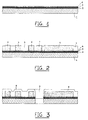
- With reference to FIG. 1 a
flat substrate 1 of, for example, alumina or other material used typically as the substrate in thin film microelectronic technology, is covered on the front with a single or double layer ofresistive metal 2, e.g. tantalium or compounds thereof with nitrogen and oxygen, followed by ametal adhesion layer 3, e.g. of titanium, and by aconductive layer 4, e.g. of palladium. - Said layers are deposited in a vacuum chamber by one of the processes of the art known by the acronym PVD (Physical Vapor Deposition), e.g. the process described in U.S. Patent no. 4226932 granted 7 October 1980.
- On the back of the substrate no deposition is made.
- There is thus obtained a product which can be stored as a semifinished product.
- The semifinished product is then taken from storage and sent to further processing, e.g. to secure a thin film hybrid circuit having certain conductive and/or resistive paths in accordance with the known art.
- With reference to FIG. 2 the
conductive layer 4 is first covered with alacquer 5 photosensitive to ultraviolet radiation hereinafter called photoresist. It is then exposed with a mask, not shown in the figure, which reproduces the paths it is wished to create, developed and grown electrogalvanically with a conductingmetal 6, e.g. gold, in the zones where the photoresist was removed during development. Either negative or positive photoresist may be used. - The growth of conducting metal, indicated by the number 7 in the figure, is also performed as a datum point allowing perfect centering of the holes it is intended to make in the circuit.
- With reference to FIG. 3, after the growth phase the
photoresist 5 is removed chemically or in plasma and the front is covered with aprotective lacquer 8 and then drilled (e.g. by ultrasonic drill, laser, diamond-tipped milling cutter), securing through holes such as those indicated byreference number 9. - The cross section of the holes may be of any form, e.g. round or elliptical.
- The
protective lacquer 8 prevents deposition of processing residue and damage to the metals, especially those in the zones surrounding the hole edges, during drilling, which must be very accurate and precise. - The
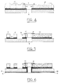
protective lacquer 8 is then removed chemically and the product thus obtained is ready for the subsequent operations which will provide conductive metallization passing through the holes and recesses in accordance with the process described below which is the object of the present invention. - With reference to FIG. 4 a cover is made with
negative photoresist 10 which is then exposed with an appropriate mask, not shown in the figure, in such a manner that after development there remain rings of themetal 6 deposited on the front and coinciding with the holes. The letter D indicates the diameter of a ring made in thephotoresist 10. - The need to use a negative photoresist is dictated by the assurance that this type of photoresist can be completely removed from the inside of the hole by using the appropriate mask for exposure so that the ring is completely free from residual photoresist.
- In the next phase metal is grown galvanically in the zone unprotected by the
photoresist 10, being careful to superimpose it on themetal 6 already deposited. - A
metal rivet 11 is thus generated as shown in FIG. 5 which protrudes toward the interior of thehole 9 because there is no photoresist to restrict its growth. Consequently the diameter of the hole is slightly reduced (by a few micron), where it coincides with the rivet, to approximately double the thickness of the grown metal. This protruding rivet assures securing reliably through the hole conductive connection with the back of the substrate. - The
negative photoresist 10 is then removed chemically and the conductive and resistive paths of the front are completed in accordance with the known art, e.g. described in Italian patent application no. 21126-A/86 filed 15 July 1986 (corresponding to EP-A-0256568) in which there is claimed a process for creating passive thin film circuits with resistive lines with different resistive layers formed by superimposing an upper layer with less resistivity on a lower layer with higher resistivity characterized in that it uses for the lower layer tantalium treated with a first dopant and for the upper layer titanium treated with a second dopant. - In this manner there is secured the result shown schematically in FIG. 5 in which are shown a
resistor 12 with itscontacts 13, aconductive line 14 which connects therivet 11. - The substrate is brought back to the vacuum chamber and, as shown in FIG. 6, there are deposited on the back, using the PVD technique, an
adhesion layer 15, e.g. of titanium, and aconduction layer 16, e.g. of palladium. Said layers also spread over the side walls of the hole until they meet at P the protrusion of therivet 11 to form a reliable conductive contact on the front. - The fundamental presence of the protruding rivet obviates the vacuum deposition of thick metal and the use of equipment with sophisticated movements to form the connections with the conductive paths of the front.
- The substrate is then removed from the vacuum chamber and the phase described in connection with FIG. 4 is repeated, i.e. deposition of negative photoresist, exposure with the same mask as in FIG. 4, development and galvanic growth of metal.
- As shown in FIG. 7, in this case the
metal 17 also grows over the entire back side and inside the hole, these being conductive surfaces covered by theconduction layer 16, thus completing the ground plane on the back of the hybrid thin film circuit and providing a reliable conductive connection through the hole or recess in addition to perfect adherence of the metallization to the walls of the hole. - Then removing the
negative photoresist 10 there is secured the finished circuit or product as shown in FIG. 8 where the reference numbers indicate the same components as described above. - If the circuit also calls for unmetallized holes they can be provided at the end of processing by a standard drilling and cutting process in accordance with the known art.
- It is clear that numerous variants of the process described are possible.
- For example in the phase described with reference to FIG. 7 it would be possible to deposit on the back negative photoresist and expose it with an appropriate mask in such a manner as to obtain a conductive path or particular integrated conductive forms on the back of the substrate.
- Variants are also possible in the type of conducting metal used to grow the layer 16 (FIG. 7), e.g. copper or silver. For the layer 17 (FIG. 7), combinations of copper, nickel or gold layers could be used.
Claims (13)
- Process for forming metallized holes in a dielectric substrate having conductive and/or resistive paths on one side, hereinafter referred to as the front, the other side being referred to hereinafter as the back, the process comprising basically the following steps in succession:
(a) electrogalvanic growth of the conductive paths (6, 7) delimited by a first photosensitive lacquer (5) on said front, (b) drilling of the substrate (1) and forming of holes (9), (c) covering of the front with a second negative photosensitive lacquer (10) and development with a mask such as to form uncovered rings of said conductive paths (6) coinciding with the holes (9), (d) electrogalvanic growth of metal on the front and forming of metal rivets (11) protruding inside the holes (9) as extensions of said conductive paths (6), (e) removal of said second photosensitive lacquer (10) and completing of conductive paths (13, 14) and/or resistive paths (12), (f) deposition on the back of metals (15, 16) which also spread over the side walls of said holes (9) until they join electrically with the protrusions of said metal rivets (11), (g) covering of the front with a further layer of said second photosensitive lacquer (10) and development with said mask, and (h) electrogalvanic growth of metal (17) on the back, the side walls of the holes and the front in the zones not covered by said second photosensitive lacquer. - Process in accordance with claim 1 characterized in that between said phases (a) and (b) said first photosensitive lacquer (5) is removed and said front is covered with a protective lacquer (8) which is then removed after said drilling phase (b).
- Process in accordance with claim 1 characterized in that in said phase (f) said deposition on the back is done in a vacuum and said metals constitute a first adhesion layer (15) followed by a first conduction layer (16).
- Process in accordance with claim 1 characterized in that after said phase (h) said second photosensitive lacquer (10) is removed.
- Process in accordance with claim 1 characterized in that said phase (a) is preceded by a vacuum deposition phase on said front of the substrate of metals which form a first resistive layer (2) followed by a second adhesion layer (3) and by a second conduction layer (4).
- Process in accordance with claim 5 characterized in that said first resistive layer (2) is formed of tantalium or its compounds with nitrogen and oxygen.
- Process in accordance with claims 3 or 5 characterized in that said first (15) and second (3) adhesion layers consist of titanium.
- Process in accordance with claims 3 or 5 characterized in that said first (16) and second (4) conduction layers consist of palladium.
- Process in accordance with claim 5 characterized in that said first resistive layer (2) is single or double.
- Process in accordance with claim 1 characterized in that said first photoresistive lacquer (5) is positive.
- Process in accordance with claim 1 characterized in that said first photosensitive lacquer (5) is negative.
- Process in accordance with claim 1 characterized in that said dielectric substrate (1) is alumina.
- Product obtained by the process set forth in the above claims, the product consisting of a hybrid circuit with conductive and resistive paths (12, 13, 14) on a substrate (1) having holes (9) around which there are metal rivets (11) protruding inside the holes on the front, the substrate being further provided with successive layers of covering metallization (15, 16) of the back and side walls of the holes so as to meet the protrusions of the rivets and conductive connections (17) between the back and front which extend between said rivets and said covering metallization.
Priority Applications (1)
| Application Number | Priority Date | Filing Date | Title |
|---|---|---|---|
| AT89200550T ATE91061T1 (en) | 1988-03-18 | 1989-03-06 | PROCESS FOR MAKING METALLIZED HOLES IN A SUBSTRATE BY METAL DEPOSITION IN VACUUM AND PRODUCT MANUFACTURED IN THIS WAY. |
Applications Claiming Priority (2)
| Application Number | Priority Date | Filing Date | Title |
|---|---|---|---|
| IT8819830A IT1216135B (en) | 1988-03-18 | 1988-03-18 | DIELECTRIC BY MEANS OF PROCESSES FOR THE EMPTYING OF METAL VACUUM, AND RELATIVE METAL HOLES IN A SUBSTRATE PRODUCT OBTAINED. |
| IT1983088 | 1988-03-18 |
Publications (3)
| Publication Number | Publication Date |
|---|---|
| EP0333252A2 EP0333252A2 (en) | 1989-09-20 |
| EP0333252A3 EP0333252A3 (en) | 1990-09-05 |
| EP0333252B1 true EP0333252B1 (en) | 1993-06-23 |
Family
ID=11161637
Family Applications (1)
| Application Number | Title | Priority Date | Filing Date |
|---|---|---|---|
| EP89200550A Expired - Lifetime EP0333252B1 (en) | 1988-03-18 | 1989-03-06 | Process for making metallized holes in a dielectric substrate by vacuum deposition of metals and the product obtained thereby |
Country Status (9)
| Country | Link |
|---|---|
| US (1) | US5011761A (en) |
| EP (1) | EP0333252B1 (en) |
| AT (1) | ATE91061T1 (en) |
| AU (1) | AU618584B2 (en) |
| DE (1) | DE68907237T2 (en) |
| ES (1) | ES2041394T3 (en) |
| IT (1) | IT1216135B (en) |
| NO (1) | NO175610C (en) |
| ZA (1) | ZA891890B (en) |
Families Citing this family (7)
| Publication number | Priority date | Publication date | Assignee | Title |
|---|---|---|---|---|
| US5584956A (en) * | 1992-12-09 | 1996-12-17 | University Of Iowa Research Foundation | Method for producing conductive or insulating feedthroughs in a substrate |
| DE69408298D1 (en) * | 1993-12-22 | 1998-03-05 | Italtel Spa | Process for producing metallized holes in dielectric substrates with interconnected thin-film conductor and / or resistance tracks |
| DE19524099A1 (en) * | 1995-07-01 | 1997-01-02 | Karlsruhe Forschzent | Process for the production of mold inserts |
| US7479304B2 (en) * | 2002-02-14 | 2009-01-20 | Applied Materials, Inc. | Gas distribution plate fabricated from a solid yttrium oxide-comprising substrate |
| ITTO20030846A1 (en) * | 2003-10-28 | 2005-04-29 | Intier Automotive Closures Spa | PROCEDURE FOR THE CONSTRUCTION OF A SUPPORTING BODY FOR A LOCK OF A MOTOR VEHICLE AND SUPPORT BODY OBTAINED. |
| US10242888B2 (en) | 2007-04-27 | 2019-03-26 | Applied Materials, Inc. | Semiconductor processing apparatus with a ceramic-comprising surface which exhibits fracture toughness and halogen plasma resistance |
| US10622194B2 (en) | 2007-04-27 | 2020-04-14 | Applied Materials, Inc. | Bulk sintered solid solution ceramic which exhibits fracture toughness and halogen plasma resistance |
Family Cites Families (4)
| Publication number | Priority date | Publication date | Assignee | Title |
|---|---|---|---|---|
| US4226932A (en) * | 1979-07-05 | 1980-10-07 | Gte Automatic Electric Laboratories Incorporated | Titanium nitride as one layer of a multi-layered coating intended to be etched |
| DE3427015A1 (en) * | 1984-07-21 | 1986-01-30 | Nippon Mektron, Ltd., Tokio/Tokyo | METHOD FOR PRODUCING VIA CONTACTS IN PRINTED CIRCUITS |
| IT1191680B (en) * | 1986-03-19 | 1988-03-23 | Gte Telecom Spa | PROCESS FOR THE REALIZATION OF METALLIC HOLES IN A SUBSTRATE EQUIPPED WITH CONDUCTIVE AND RESISTIVE PATHS, AND PRODUCT OBTAINED WITH THE ABOVE PROCESS |
| IT1197776B (en) * | 1986-07-15 | 1988-12-06 | Gte Telecom Spa | PROCESS FOR OBTAINING THIN LAYER PASSIVE CIRCUITS WITH RESISTIVE LINES TO DIFFERENT LAYER RESISTANCE AND PASSIVE CIRCUIT REALIZED WITH THE ABOVE PROCESS |
-
1988
- 1988-03-18 IT IT8819830A patent/IT1216135B/en active
-
1989
- 1989-02-27 US US07/316,365 patent/US5011761A/en not_active Expired - Fee Related
- 1989-03-06 EP EP89200550A patent/EP0333252B1/en not_active Expired - Lifetime
- 1989-03-06 DE DE89200550T patent/DE68907237T2/en not_active Expired - Fee Related
- 1989-03-06 ES ES198989200550T patent/ES2041394T3/en not_active Expired - Lifetime
- 1989-03-06 AT AT89200550T patent/ATE91061T1/en not_active IP Right Cessation
- 1989-03-09 AU AU31179/89A patent/AU618584B2/en not_active Ceased
- 1989-03-13 ZA ZA891890A patent/ZA891890B/en unknown
- 1989-03-16 NO NO891153A patent/NO175610C/en unknown
Also Published As
| Publication number | Publication date |
|---|---|
| US5011761A (en) | 1991-04-30 |
| NO175610C (en) | 1994-11-02 |
| NO891153L (en) | 1989-09-19 |
| AU618584B2 (en) | 1992-01-02 |
| EP0333252A3 (en) | 1990-09-05 |
| IT1216135B (en) | 1990-02-22 |
| AU3117989A (en) | 1989-09-21 |
| ZA891890B (en) | 1989-11-29 |
| NO175610B (en) | 1994-07-25 |
| DE68907237T2 (en) | 1993-12-02 |
| IT8819830A0 (en) | 1988-03-18 |
| ATE91061T1 (en) | 1993-07-15 |
| NO891153D0 (en) | 1989-03-16 |
| ES2041394T3 (en) | 1993-11-16 |
| DE68907237D1 (en) | 1993-07-29 |
| EP0333252A2 (en) | 1989-09-20 |
Similar Documents
| Publication | Publication Date | Title |
|---|---|---|
| US4810332A (en) | Method of making an electrical multilayer copper interconnect | |
| US4272561A (en) | Hybrid process for SBD metallurgies | |
| KR100304317B1 (en) | Method of forming raised metallic contacts on electrical circuits | |
| US4054484A (en) | Method of forming crossover connections | |
| US5662788A (en) | Method for forming a metallization layer | |
| EP0099544B1 (en) | Method for forming conductive lines and via studs on lsi carrier substrates | |
| EP0083397B1 (en) | Methods of forming electronic microcircuits | |
| US5985521A (en) | Method for forming electrically conductive layers on chip carrier substrates having through holes or via holes | |
| EP0362161B1 (en) | Method of manufacturing a substrate for microwave integrated circuits | |
| JPS6239846B2 (en) | ||
| US4964947A (en) | Method of manufacturing double-sided wiring substrate | |
| JPH0213949B2 (en) | ||
| GB1527108A (en) | Methods of forming conductors on substrates involving electroplating | |
| US4118523A (en) | Production of semiconductor devices | |
| US5011761A (en) | Process for making metallized holes in a dielectric substrate by vacuum deposition of metals and the product obtained thereby | |
| US3745094A (en) | Two resist method for printed circuit structure | |
| EP0088869B1 (en) | Thin film techniques for fabricating narrow track ferrite heads | |
| US5200300A (en) | Methods for forming high density multi-chip carriers | |
| EP0112898A1 (en) | Making solderable printed circuit boards | |
| US5922517A (en) | Method of preparing a substrate surface for conformal plating | |
| JPH05502138A (en) | Interconnects in multilayer wiring and methods of forming them | |
| US4011144A (en) | Methods of forming metallization patterns on beam lead semiconductor devices | |
| EP0670668B1 (en) | Process for the provision of metallized holes in dielectric substrates comprising interconnected thin film conductive and/or resistive paths | |
| US5980721A (en) | Fabrication method for double metallic resist printed circuit boards | |
| US3811973A (en) | Technique for the fabrication of a bilevel thin film integrated circuit |
Legal Events
| Date | Code | Title | Description |
|---|---|---|---|
| PUAI | Public reference made under article 153(3) epc to a published international application that has entered the european phase |
Free format text: ORIGINAL CODE: 0009012 |
|
| AK | Designated contracting states |
Kind code of ref document: A2 Designated state(s): AT BE CH DE ES FR GB IT LI NL SE |
|
| PUAL | Search report despatched |
Free format text: ORIGINAL CODE: 0009013 |
|
| AK | Designated contracting states |
Kind code of ref document: A3 Designated state(s): AT BE CH DE ES FR GB IT LI NL SE |
|
| 17P | Request for examination filed |
Effective date: 19901121 |
|
| 17Q | First examination report despatched |
Effective date: 19920623 |
|
| GRAA | (expected) grant |
Free format text: ORIGINAL CODE: 0009210 |
|
| AK | Designated contracting states |
Kind code of ref document: B1 Designated state(s): AT BE CH DE ES FR GB IT LI NL SE |
|
| REF | Corresponds to: |
Ref document number: 91061 Country of ref document: AT Date of ref document: 19930715 Kind code of ref document: T |
|
| ITF | It: translation for a ep patent filed | ||
| REF | Corresponds to: |
Ref document number: 68907237 Country of ref document: DE Date of ref document: 19930729 |
|
| ET | Fr: translation filed | ||
| REG | Reference to a national code |
Ref country code: ES Ref legal event code: FG2A Ref document number: 2041394 Country of ref document: ES Kind code of ref document: T3 |
|
| PLBE | No opposition filed within time limit |
Free format text: ORIGINAL CODE: 0009261 |
|
| STAA | Information on the status of an ep patent application or granted ep patent |
Free format text: STATUS: NO OPPOSITION FILED WITHIN TIME LIMIT |
|
| 26N | No opposition filed | ||
| EAL | Se: european patent in force in sweden |
Ref document number: 89200550.5 |
|
| PGFP | Annual fee paid to national office [announced via postgrant information from national office to epo] |
Ref country code: GB Payment date: 19960220 Year of fee payment: 8 |
|
| PGFP | Annual fee paid to national office [announced via postgrant information from national office to epo] |
Ref country code: AT Payment date: 19960223 Year of fee payment: 8 |
|
| PGFP | Annual fee paid to national office [announced via postgrant information from national office to epo] |
Ref country code: ES Payment date: 19960311 Year of fee payment: 8 |
|
| PGFP | Annual fee paid to national office [announced via postgrant information from national office to epo] |
Ref country code: BE Payment date: 19960319 Year of fee payment: 8 |
|
| PGFP | Annual fee paid to national office [announced via postgrant information from national office to epo] |
Ref country code: SE Payment date: 19960320 Year of fee payment: 8 |
|
| PGFP | Annual fee paid to national office [announced via postgrant information from national office to epo] |
Ref country code: NL Payment date: 19960328 Year of fee payment: 8 Ref country code: FR Payment date: 19960328 Year of fee payment: 8 |
|
| PGFP | Annual fee paid to national office [announced via postgrant information from national office to epo] |
Ref country code: DE Payment date: 19960520 Year of fee payment: 8 |
|
| PGFP | Annual fee paid to national office [announced via postgrant information from national office to epo] |
Ref country code: CH Payment date: 19960624 Year of fee payment: 8 |
|
| PG25 | Lapsed in a contracting state [announced via postgrant information from national office to epo] |
Ref country code: GB Effective date: 19970306 Ref country code: AT Effective date: 19970306 |
|
| PG25 | Lapsed in a contracting state [announced via postgrant information from national office to epo] |
Ref country code: SE Effective date: 19970307 Ref country code: ES Free format text: LAPSE BECAUSE OF NON-PAYMENT OF DUE FEES Effective date: 19970307 |
|
| PG25 | Lapsed in a contracting state [announced via postgrant information from national office to epo] |
Ref country code: LI Effective date: 19970331 Ref country code: CH Effective date: 19970331 Ref country code: BE Effective date: 19970331 |
|
| BERE | Be: lapsed |
Owner name: SIEMENS TELECOMUNICAZIONI S.P.A. Effective date: 19970331 |
|
| PG25 | Lapsed in a contracting state [announced via postgrant information from national office to epo] |
Ref country code: NL Effective date: 19971001 |
|
| GBPC | Gb: european patent ceased through non-payment of renewal fee |
Effective date: 19970306 |
|
| REG | Reference to a national code |
Ref country code: CH Ref legal event code: PL |
|
| PG25 | Lapsed in a contracting state [announced via postgrant information from national office to epo] |
Ref country code: FR Free format text: LAPSE BECAUSE OF NON-PAYMENT OF DUE FEES Effective date: 19971128 |
|
| NLV4 | Nl: lapsed or anulled due to non-payment of the annual fee |
Effective date: 19971001 |
|
| PG25 | Lapsed in a contracting state [announced via postgrant information from national office to epo] |
Ref country code: DE Effective date: 19971202 |
|
| EUG | Se: european patent has lapsed |
Ref document number: 89200550.5 |
|
| REG | Reference to a national code |
Ref country code: FR Ref legal event code: ST |
|
| REG | Reference to a national code |
Ref country code: ES Ref legal event code: FD2A Effective date: 19990405 |
|
| PG25 | Lapsed in a contracting state [announced via postgrant information from national office to epo] |
Ref country code: IT Free format text: LAPSE BECAUSE OF NON-PAYMENT OF DUE FEES;WARNING: LAPSES OF ITALIAN PATENTS WITH EFFECTIVE DATE BEFORE 2007 MAY HAVE OCCURRED AT ANY TIME BEFORE 2007. THE CORRECT EFFECTIVE DATE MAY BE DIFFERENT FROM THE ONE RECORDED. Effective date: 20050306 |