EP0332431A2 - Logarithmic amplifier - Google Patents
Logarithmic amplifier Download PDFInfo
- Publication number
- EP0332431A2 EP0332431A2 EP89302324A EP89302324A EP0332431A2 EP 0332431 A2 EP0332431 A2 EP 0332431A2 EP 89302324 A EP89302324 A EP 89302324A EP 89302324 A EP89302324 A EP 89302324A EP 0332431 A2 EP0332431 A2 EP 0332431A2
- Authority
- EP
- European Patent Office
- Prior art keywords
- transmission line
- gate
- low pass
- lpf8
- logarithmic amplifier
- Prior art date
- Legal status (The legal status is an assumption and is not a legal conclusion. Google has not performed a legal analysis and makes no representation as to the accuracy of the status listed.)
- Withdrawn
Links
Images

Classifications
-
- G—PHYSICS
- G06—COMPUTING; CALCULATING OR COUNTING
- G06G—ANALOGUE COMPUTERS
- G06G7/00—Devices in which the computing operation is performed by varying electric or magnetic quantities
- G06G7/12—Arrangements for performing computing operations, e.g. operational amplifiers
- G06G7/24—Arrangements for performing computing operations, e.g. operational amplifiers for evaluating logarithmic or exponential functions, e.g. hyperbolic functions
-
- H—ELECTRICITY
- H03—ELECTRONIC CIRCUITRY
- H03G—CONTROL OF AMPLIFICATION
- H03G7/00—Volume compression or expansion in amplifiers
- H03G7/001—Volume compression or expansion in amplifiers without controlling loop
Definitions
- Logarithmic amplifiers which are amplifiers having a logarithmic transfer characteristic, are used widely and one example of their use is in microwave instrumentation.
- At present logarithmic amplifiers comprise a number of amplifiers having a linear characteristic connected sequentially via hybrid couplers.
- Each of the hybrid couplers is connected to a demodulator for demodulating an amplitude modulated signal and these are commonly known as video detectors.
- the outputs from all of the demodulators are then summed to provide the logarithmic output of the amplifier.
- a logarithmic amplifier comprises a series of MESFET distributed amplifiers connected in cascade, each of the MESFET distributed amplifiers having a gate transmission line and a drain transmission line which share a common ground or source line, a number of MESFETs connected in parallel with their gate electrodes connected at spaced intervals along the gate transmission line, their drain electrodes connected at spaced intervals along the drain transmission line and their source electrodes connected to the source line; a low pass filter connected to the downstream end of the gate transmission line of each distributed amplifier, each low pass filter passing only the rectified component of the travelling wave passing along each gate transmission line; and, a summer connected to the outputs of each of the low pass filters to sum them and provide an output, the output of the summer providing the output of the logarithmic amplifier.
- This rectified output is DC for a constant carrier wave and a demodulated signal for an amplitude modulated carrier wave.
- the rectified output is invariant once the amplifier has been driven into saturation. Prior to saturation no rectification and therefore no d.c. or demodulated signal appears across the gate source diode.
- the invariant output of the or each distributed amplifier passes through its or their associated low-pass filters and are then summed in the summer to provide the output from the logarithmic amplifier.
- the gate transmission line of each distributed amplifier includes decoupling capacitors between the transmission line and impedance matching loads connected to the ends of each gate transmission line and, in this case, the low pass filter is connected to the downstream end of each gate transmission line immediately upstream of the decoupling capacitor.
- the low pass filter may be formed by a simple L-C circuit to pass only a low frequency component corresponding to an amplitude modulation applied to the signal carried by the gate transmission line.
- the summer is preferably formed by a multi-input operational amplifier having the outputs from each of the low pass filters connected to its inputs.
- MESFET distributed amplifiers have a very broad bandwidth and accordingly a logarithmic amplifier in accordance with this invention is capable of handling pulses having a very short rise time of the order of tens of picoseconds.
- GaAs MESFET distributed amplifiers capable of handling signals from 20 MHz to 50 GHz are relatively cheap and can be readily formed as a monolithic integrated circuit or a hybrid integrated circuit in which all of the components are manufactured separately and then mounted on a microwave substrate.
- the number of distributed amplifiers connected in cascade depends upon the required dynamic range of the logarithmic amplifier. Typically distributed amplifiers including, for example, four GaAs MESFETs have a gain of between 6 and 10 dB. Thus, for a logarithmic amplifier to have a dynamic range of 70 dB, 7 to 12 distributed amplifiers are connected together in cascade. Typically 8 or 9 amplifiers are connected together.
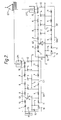
- This example of a logarithmic amplifier includes eight distributed amplifiers DA1 to DA8 connected together in cascade. Each distributed amplifier DA1 to DA8 has the downstream end of its gate transmission line connected to low pass filters LP1 to LP8 and the outputs of these are connected to a summer OP1.
- Each distributed amplifier includes four GaAs MESFETs 1 to 4 with their gate electrodes connected to a gate transmission line G, their drain electrodes connected to a drain transmission line D and their source electrodes connected to a ground plane 5.
- An input 6 to the first distributed amplifier DA1 forms the input to the logarithmic amplifier.
- the gate transmission lines G include decoupling capacitors 7, inductors 8 connected between the gate electrodes of successive transistors 1, 2, 3 and 4 and inductors 10 in the end sections of the line.
- the drain transmission line D includes inductors 9 connected between the drain electrodes of adjacent transistors 1, 2, 3 and 4 and inductors 11 in the end sections of the line.
- the gate transmission line G is terminated at its downstream end, the right hand end, as seen in Figure 2, by a resistor 12 which matches the characteristic impedance of the line.
- the left hand side of the gate transmission line is terminated by a generator 13 whose signal is to be amplified and which has a source impedance equal to the gate line characteristic impedance.
- the drain transmission line D includes at its left hand end a resistor 14 matching the characteristic impedance of the line.
- a DC source 15 is connected to the source line 5 and to the junction of the resistor 14 and adjacent inductor 11 via a low pass filter 16 to provide bias, typically reverse bias, for the drain electrodes of the transistors 1 to 4.
- a microwave signal fed into the input 6 by the generator 13 is amplified by the successive transistors 1 to 4. Typically with four transistors a gain of 6 dB is obtained in each distributed amplifier.
- the travelling wave moving along the gate transmission line G is picked off at a node between the inductor 10 and the decoupling capacitor 7 and fed to a low pass filter LP1 to LP8.
- These low pass filters allow only low frequency and d.c components to pass through.
- the outputs from the low pass filters LP1 to LP8 are fed to eight adding inputs of a summer formed by an operational amplifier OP1.
- the right hand end of the drain transmission line D of distributed amplifier DA1 is connected across the input 6 of distributed amplifier DA2 to connect the amplifiers DA1 and DA2 in cascade. This connection is repeated throughout all of the stages. All of the distributed amplifiers DA1 to DA8 and low pass filters LP1 to LP8 are similar except that the right hand end of the drain transmission line D8 in distributed amplifier DA8 is terminated by an impedance matching resistor (not shown) the resistance of which matches the characteristic impedance of that of the drain transmission line D.
- the gate source junction at least partly rectifies the microwave signal travelling along the gate transmission line G to produce a demodulated signal consisting of a demodulated signal corresponding to the amplitude modulation on the signal and a d.c. component corresponding to the rectified carrier wave signal.
- the frequency of the demodulated signal is much lower than that of the microwave signal and this and the d.c. component is passed by the low-pass filter LPF6 to the summer OP1.
- the rectified and demodulated signals from the distributed amplifiers DA7 and DA8 are passed by the low-pass filters LPF7 and LPF8, and all are then summed in summer OP1 to provide the logarithmic output log o/p.
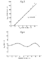
- Figures 3 and 4 illustrate the output of a simple three stage demonstration logarithmic amplifier in accordance with this invention.
- Figure 3 is a graph of the peak output voltage against the input power in dB illustrating the performance of the amplifier at a frequency of 8 GHz with a pulse width of 2 microseconds and a pulse repetition frequency of 100 KHz.
- Figure 4 illustrates the variation in the input power required to give a constant output of 200 mV with frequency over a frequency range from 2 to 18 GHz and shows that, over this frequency range the logarithmic transfer function is substantially constant.
- Figures 5A to 5B illustrate the linearity of a nine module log amplifier in accordance with this invention over a dynamic range of 70 dB at operating frequencies of 2 and 4 GHz, respectively.
Abstract
Logarithmic amplifiers which have a logarithmic transfer characteristic may be used in microwave instrumentation. Such an amplifier includes a series of MESFET distributed amplifiers (DA1-DA8) connected in cascade, with each of the MESFET distributed amplifiers (DA1-DA8) having a gate transmission line (G1-G8) and a drain transmission line (D1-D8) which share a common ground or source line (5), and a number of MESFETs (1-4) connected in parallel with their gate electrodes (g) connected at spaced intervals along the gate transmission line (G1-G8), their drain electrodes (d) connected at spaced intervals along the drain transmission line (D1-D8) and their source electrodes (s) connected to the source line (5). A low pass filter (LPF1-LPF8) is connected to the downstream end of the gate transmission line (G1-G8) of each distributed amplifier (DAl-DA8) with each low pass filter (LPF1-LPF8) passing only the rectified component of the travelling wave passing along each gate transmission line (G1-G8). A summer (OP1) is connected to the outputs of each of the low pass filters (LPF4-LPF8) to sum them and provide an output (O/P) which provides the output of the logarithmic amplifier.
Description
- Logarithmic amplifiers which are amplifiers having a logarithmic transfer characteristic, are used widely and one example of their use is in microwave instrumentation.
- At present logarithmic amplifiers comprise a number of amplifiers having a linear characteristic connected sequentially via hybrid couplers. Each of the hybrid couplers is connected to a demodulator for demodulating an amplitude modulated signal and these are commonly known as video detectors. The outputs from all of the demodulators are then summed to provide the logarithmic output of the amplifier.
- It is also known to use a single amplifier with a linear characteristic and then to apply the output of the linear amplifier to a demodulator for demodulating an amplitude modulated signal with the demodulator itself having a logarithmic transfer characteristic so that the output from the demodulator provides the logarithmic output from the amplifier.
- Conventional linear amplifiers for operating at microwave frequencies usually include both a resonant input stage and a resonant output stage and accordingly they, and any resulting logarithmic amplifier including them, only has a limited bandwidth. This gives rise to difficulties when the resulting logarithmic amplifiers are required to handle short pulses for which a large bandwidth is required. Amplifiers capable of operating at microwave frequencies are expensive and previous attempts to improve their bandwidth have resulted in the further increase in their cost.
- According to this invention a logarithmic amplifier comprises a series of MESFET distributed amplifiers connected in cascade, each of the MESFET distributed amplifiers having a gate transmission line and a drain transmission line which share a common ground or source line, a number of MESFETs connected in parallel with their gate electrodes connected at spaced intervals along the gate transmission line, their drain electrodes connected at spaced intervals along the drain transmission line and their source electrodes connected to the source line; a low pass filter connected to the downstream end of the gate transmission line of each distributed amplifier, each low pass filter passing only the rectified component of the travelling wave passing along each gate transmission line; and, a summer connected to the outputs of each of the low pass filters to sum them and provide an output, the output of the summer providing the output of the logarithmic amplifier.
- As a signal input into the first of the distributed amplifiers passes through the series of distributed amplifiers it is increased in level until saturation occurs in one of them. For a gradually increasing input signal it is the final distributed amplifier which saturates first, followed in turn by the penultimate, the antepenultimate and so on. Once saturation occurs the output of that amplifier is invariant. The cause of saturation is that the gate source diode of the MESFETs in the distributed amplifier, initially the final one, and subsequently the other ones, operates non-linearly. Thus the signal level of the signal carried by that MESFET is sufficient to drive its gate source junction into conduction. Thus the gate source junction rectifies and produces a rectified output on the gate transmission line. This rectified output is DC for a constant carrier wave and a demodulated signal for an amplitude modulated carrier wave. The rectified output is invariant once the amplifier has been driven into saturation. Prior to saturation no rectification and therefore no d.c. or demodulated signal appears across the gate source diode. The invariant output of the or each distributed amplifier passes through its or their associated low-pass filters and are then summed in the summer to provide the output from the logarithmic amplifier.
- Preferably the gate transmission line of each distributed amplifier includes decoupling capacitors between the transmission line and impedance matching loads connected to the ends of each gate transmission line and, in this case, the low pass filter is connected to the downstream end of each gate transmission line immediately upstream of the decoupling capacitor. The low pass filter may be formed by a simple L-C circuit to pass only a low frequency component corresponding to an amplitude modulation applied to the signal carried by the gate transmission line. The summer is preferably formed by a multi-input operational amplifier having the outputs from each of the low pass filters connected to its inputs.
- MESFET distributed amplifiers have a very broad bandwidth and accordingly a logarithmic amplifier in accordance with this invention is capable of handling pulses having a very short rise time of the order of tens of picoseconds. GaAs MESFET distributed amplifiers capable of handling signals from 20 MHz to 50 GHz are relatively cheap and can be readily formed as a monolithic integrated circuit or a hybrid integrated circuit in which all of the components are manufactured separately and then mounted on a microwave substrate.
- The number of distributed amplifiers connected in cascade depends upon the required dynamic range of the logarithmic amplifier. Typically distributed amplifiers including, for example, four GaAs MESFETs have a gain of between 6 and 10 dB. Thus, for a logarithmic amplifier to have a dynamic range of 70 dB, 7 to 12 distributed amplifiers are connected together in cascade. Typically 8 or 9 amplifiers are connected together.
- A particular example of a logarithmic amplifier in accordance with this invention will now be described with reference to the accompanying drawings, in which:
- Figure 1 is a block diagram of the logarithmic amplifier;
- Figure 2 is a circuit diagram of part of the logarithmic amplifier showing the construction of the first and second distributed amplifier;
- Figure 3 is a graph of output voltage against input power;
- Figure 4 is a graph of input power against frequency; and,
- Figures 5A and 5B are graphs illustrating the linearity of a nine module log amplifier operating at 2 GHz and 4 GHz respectively.
- This example of a logarithmic amplifier includes eight distributed amplifiers DA1 to DA8 connected together in cascade. Each distributed amplifier DA1 to DA8 has the downstream end of its gate transmission line connected to low pass filters LP1 to LP8 and the outputs of these are connected to a summer OP1.
- Each distributed amplifier includes four
GaAs MESFETs 1 to 4 with their gate electrodes connected to a gate transmission line G, their drain electrodes connected to a drain transmission line D and their source electrodes connected to aground plane 5. Aninput 6 to the first distributed amplifier DA1 forms the input to the logarithmic amplifier. - The gate transmission lines G include
decoupling capacitors 7,inductors 8 connected between the gate electrodes ofsuccessive transistors inductors 10 in the end sections of the line. The drain transmission line D includesinductors 9 connected between the drain electrodes ofadjacent transistors inductors 11 in the end sections of the line. The gate transmission line G is terminated at its downstream end, the right hand end, as seen in Figure 2, by aresistor 12 which matches the characteristic impedance of the line. The left hand side of the gate transmission line is terminated by agenerator 13 whose signal is to be amplified and which has a source impedance equal to the gate line characteristic impedance. The drain transmission line D includes at its left hand end aresistor 14 matching the characteristic impedance of the line. ADC source 15 is connected to thesource line 5 and to the junction of theresistor 14 andadjacent inductor 11 via alow pass filter 16 to provide bias, typically reverse bias, for the drain electrodes of thetransistors 1 to 4. - In use a microwave signal fed into the
input 6 by thegenerator 13 is amplified by thesuccessive transistors 1 to 4. Typically with four transistors a gain of 6 dB is obtained in each distributed amplifier. The travelling wave moving along the gate transmission line G is picked off at a node between theinductor 10 and thedecoupling capacitor 7 and fed to a low pass filter LP1 to LP8. These low pass filters allow only low frequency and d.c components to pass through. The outputs from the low pass filters LP1 to LP8 are fed to eight adding inputs of a summer formed by an operational amplifier OP1. - The right hand end of the drain transmission line D of distributed amplifier DA1 is connected across the
input 6 of distributed amplifier DA2 to connect the amplifiers DA1 and DA2 in cascade. This connection is repeated throughout all of the stages. All of the distributed amplifiers DA1 to DA8 and low pass filters LP1 to LP8 are similar except that the right hand end of the drain transmission line D8 in distributed amplifier DA8 is terminated by an impedance matching resistor (not shown) the resistance of which matches the characteristic impedance of that of the drain transmission line D. - As the microwave signal fed into the distributed amplifier DA1 passes through the cascaded amplifiers DA1 to DA8 its amplitude increases in each distributed amplifier until saturation of one or of one MESFET in one of the amplifiers occurs. With a very small input microwave signal saturation will occur in amplifier DA8 and with the smallest signal, saturation only of
MESFET 4 in amplifier DA8. As the input signal level increases more MESFETs in more amplifiers are saturated. Consider a typical case where saturation occurs in at least one of theMESFETs 1 to 4, in amplifier DA6.MESFET 4 saturates first and operates non-linearly because the gate source diode of this MESFET has been driven into conduction. Under these conditions the gate source junction at least partly rectifies the microwave signal travelling along the gate transmission line G to produce a demodulated signal consisting of a demodulated signal corresponding to the amplitude modulation on the signal and a d.c. component corresponding to the rectified carrier wave signal. The frequency of the demodulated signal is much lower than that of the microwave signal and this and the d.c. component is passed by the low-pass filter LPF6 to the summer OP1. Similarly the rectified and demodulated signals from the distributed amplifiers DA7 and DA8 are passed by the low-pass filters LPF7 and LPF8, and all are then summed in summer OP1 to provide the logarithmic output log o/p. - Figures 3 and 4 illustrate the output of a simple three stage demonstration logarithmic amplifier in accordance with this invention. Figure 3 is a graph of the peak output voltage against the input power in dB illustrating the performance of the amplifier at a frequency of 8 GHz with a pulse width of 2 microseconds and a pulse repetition frequency of 100 KHz. Figure 4 illustrates the variation in the input power required to give a constant output of 200 mV with frequency over a frequency range from 2 to 18 GHz and shows that, over this frequency range the logarithmic transfer function is substantially constant.
- Figures 5A to 5B illustrate the linearity of a nine module log amplifier in accordance with this invention over a dynamic range of 70 dB at operating frequencies of 2 and 4 GHz, respectively.
Claims (7)
1. A logarithmic amplifier comprising a series of MESFET distributed amplifiers (DA1-DA8) connected in cascade, each of the MESFET distributed amplifiers (DA1-DA8) having a gate transmission line (G1-G8) and a drain transmission line (D1-D8) which share a common ground or source line (5), a number of MESFETs (1, 2, 3, 4) connected in parallel with their gate electrodes (g) connected at spaced intervals along the gate transmission line (G1-G8), their drain electrodes (d) connected at spaced intervals along the drain transmission line (D1-D8) and their source electrodes (s) connected to the source line (5);
characterised in that the logarithmic amplifier also includes a low pass filter (LPF1-LPF8) connected to the downstream end of the gate transmission line (G1-G8) of each distributed amplifier (DA1-DA8), each low pass filter (LPF1-LPF8) passing only the rectified component of the travelling wave passing along each gate transmission line (G1-G8), and a summer (OP1) connected to the outputs of each of the low pass filters (LPF1-LPF8) to sum them and provide an output (O/P), the output (O/P) of the summer (OP1) providing the output of the logarithmic amplifier.
characterised in that the logarithmic amplifier also includes a low pass filter (LPF1-LPF8) connected to the downstream end of the gate transmission line (G1-G8) of each distributed amplifier (DA1-DA8), each low pass filter (LPF1-LPF8) passing only the rectified component of the travelling wave passing along each gate transmission line (G1-G8), and a summer (OP1) connected to the outputs of each of the low pass filters (LPF1-LPF8) to sum them and provide an output (O/P), the output (O/P) of the summer (OP1) providing the output of the logarithmic amplifier.
2. A logarithmic amplifier according to claim 1, in which the gate transmission line (G1-G8) of each distributed amplifier (DA1-DA8) includes decoupling capacitors (7) between the transmission line (G1-G8) and impedance matching loads (12) connected to the ends of each gate transmission line (Gl-G8) and, in which the low pass filter (LPF1-LPF8) is connected to the downstream end of each gate transmission line immediately upstream of the decoupling capacitor (7).
3. A logarithmic amplifier according to claim 1 or 2, in which each low pass filter (LPF1-LPF8) is formed by a simple L-C circuit to pass only a low frequency component corresponding to an amplitude modulation and d.c. component of the signal carried by each gate transmission line (G1-G8).
4. A logarithmic amplifier according to any preceding claim, in which the summer is formed by a multi-input operational amplifier (OP1) having the outputs from each of the low pass filters (LPF1-LPF8) connected to its inputs.
5. A logarithmic amplifier according to any preceding claim, in which the MESFETS are GaAs MESFETs.
6. A logarithmic amplifier according to any preceding claim, in which each of the distributed amplifiers (DA1-DA8) connected in cascade includes four GaAs MESFETs and in which eight or nine distributed amplifiers (DA1-DA8) are connected together in cascade.
7. A logarithmic amplifier according to any preceding claim, in which the distributed amplifiers are capable of handling microwave signals having a frequency in a range from 20 MHz to 50 GHz.
Applications Claiming Priority (2)
| Application Number | Priority Date | Filing Date | Title |
|---|---|---|---|
| GB888805672A GB8805672D0 (en) | 1988-03-10 | 1988-03-10 | Logarithmic amplifier |
| GB8805672 | 1988-03-10 |
Publications (2)
| Publication Number | Publication Date |
|---|---|
| EP0332431A2 true EP0332431A2 (en) | 1989-09-13 |
| EP0332431A3 EP0332431A3 (en) | 1991-01-30 |
Family
ID=10633164
Family Applications (1)
| Application Number | Title | Priority Date | Filing Date |
|---|---|---|---|
| EP19890302324 Withdrawn EP0332431A3 (en) | 1988-03-10 | 1989-03-09 | Logarithmic amplifier |
Country Status (3)
| Country | Link |
|---|---|
| US (1) | US4885483A (en) |
| EP (1) | EP0332431A3 (en) |
| GB (1) | GB8805672D0 (en) |
Cited By (2)
| Publication number | Priority date | Publication date | Assignee | Title |
|---|---|---|---|---|
| EP0629043A1 (en) * | 1993-06-11 | 1994-12-14 | Nec Corporation | High frequency amplifier |
| WO1997001219A1 (en) * | 1995-06-22 | 1997-01-09 | Northern Telecom Limited | A high frequency, differential limiting distributed amplifier |
Families Citing this family (4)
| Publication number | Priority date | Publication date | Assignee | Title |
|---|---|---|---|---|
| US5177381A (en) * | 1991-12-06 | 1993-01-05 | Motorola, Inc. | Distributed logarithmic amplifier and method |
| US5485118A (en) * | 1994-06-03 | 1996-01-16 | Massachusetts Institute Of Technology | Non-uniformly distributed power amplifier |
| US5689210A (en) * | 1995-09-20 | 1997-11-18 | Lange; Julius | Active distributed signal sampler |
| JP2003174338A (en) * | 2001-12-05 | 2003-06-20 | Murata Mfg Co Ltd | Distribution amplifier and distribution differential amplifier |
Citations (2)
| Publication number | Priority date | Publication date | Assignee | Title |
|---|---|---|---|---|
| US4209714A (en) * | 1977-06-13 | 1980-06-24 | Trio Kabushiki Kaisha | Logarithmic amplifier |
| US4507615A (en) * | 1982-12-16 | 1985-03-26 | Tektronix, Inc. | Non-linear amplifier systems |
Family Cites Families (1)
| Publication number | Priority date | Publication date | Assignee | Title |
|---|---|---|---|---|
| US3668535A (en) * | 1970-01-15 | 1972-06-06 | Varian Associates | Logarithmic rf amplifier employing successive detection |
-
1988
- 1988-03-10 GB GB888805672A patent/GB8805672D0/en active Pending
-
1989
- 1989-03-09 EP EP19890302324 patent/EP0332431A3/en not_active Withdrawn
- 1989-03-09 US US07/321,507 patent/US4885483A/en not_active Expired - Fee Related
Patent Citations (2)
| Publication number | Priority date | Publication date | Assignee | Title |
|---|---|---|---|---|
| US4209714A (en) * | 1977-06-13 | 1980-06-24 | Trio Kabushiki Kaisha | Logarithmic amplifier |
| US4507615A (en) * | 1982-12-16 | 1985-03-26 | Tektronix, Inc. | Non-linear amplifier systems |
Non-Patent Citations (1)
| Title |
|---|
| IEEE JOURNAL OF SOLID-STATE CIRCUITS, vol. SC-15, no. 3, June 1980, pages 291-295; W.L. BARBER et al.: "A true logarithmic amplifier for radar IF applications" * |
Cited By (3)
| Publication number | Priority date | Publication date | Assignee | Title |
|---|---|---|---|---|
| EP0629043A1 (en) * | 1993-06-11 | 1994-12-14 | Nec Corporation | High frequency amplifier |
| US5412339A (en) * | 1993-06-11 | 1995-05-02 | Nec Corporation | High frequency amplifier |
| WO1997001219A1 (en) * | 1995-06-22 | 1997-01-09 | Northern Telecom Limited | A high frequency, differential limiting distributed amplifier |
Also Published As
| Publication number | Publication date |
|---|---|
| EP0332431A3 (en) | 1991-01-30 |
| US4885483A (en) | 1989-12-05 |
| GB8805672D0 (en) | 1988-04-07 |
Similar Documents
| Publication | Publication Date | Title |
|---|---|---|
| US4896374A (en) | Broadband monolithic balanced mixer apparatus | |
| US4931921A (en) | Wide bandwidth frequency doubler | |
| US10491178B2 (en) | Parametric amplifier system | |
| US6476676B1 (en) | Semiconductor integrated circuit | |
| US5986518A (en) | Distributed MMIC active quadrature hybrid and method for providing in-phase and quadrature-phase signals | |
| US4430626A (en) | Networks for the log domain | |
| EP0602053A1 (en) | High efficiency harmonic injection power amplifier | |
| Nguyen et al. | A Si bipolar monolithic RF bandpass amplifier | |
| US4885483A (en) | Logarithmic amplifier | |
| US4406990A (en) | Direct coupled DC amplification circuit | |
| US5414313A (en) | Dual-mode logarithmic amplifier having cascaded stages | |
| US4908529A (en) | Logarithmic amplifier comprising MESFET distributed amplifiers connected in cascade | |
| US6124742A (en) | Wide bandwidth frequency multiplier | |
| US5434522A (en) | Frequency doubler circuit having a diode quad with a grounded port | |
| US4980584A (en) | Multi-stage wideband successive detection logarithmic amplifier | |
| US4845440A (en) | Distributed amplifier circuits | |
| US4491809A (en) | Matching circuit for a pre-amplifier of SHF band television signal receiver | |
| US4812780A (en) | Broadband differential amplifier | |
| US4876516A (en) | High gain distributed amplifiers | |
| US5047728A (en) | Amplifier having a low noise active GaAs MESFET load | |
| HU186327B (en) | Circuit arrangement for dampint electromagnetic disturbances in potical receivers | |
| US4319198A (en) | Power amplifiers | |
| US5093629A (en) | Amplifier circuit having second order signal cancellation | |
| EP0244973A2 (en) | Broadband differential amplifier | |
| EP0645916B1 (en) | Balanced phase modulator used in microwave band |
Legal Events
| Date | Code | Title | Description |
|---|---|---|---|
| PUAI | Public reference made under article 153(3) epc to a published international application that has entered the european phase |
Free format text: ORIGINAL CODE: 0009012 |
|
| AK | Designated contracting states |
Kind code of ref document: A2 Designated state(s): AT BE CH DE ES FR GB GR IT LI LU NL SE |
|
| PUAL | Search report despatched |
Free format text: ORIGINAL CODE: 0009013 |
|
| AK | Designated contracting states |
Kind code of ref document: A3 Designated state(s): AT BE CH DE ES FR GB GR IT LI LU NL SE |
|
| STAA | Information on the status of an ep patent application or granted ep patent |
Free format text: STATUS: THE APPLICATION IS DEEMED TO BE WITHDRAWN |
|
| 18D | Application deemed to be withdrawn |
Effective date: 19911001 |