EP0331304A2 - Amplification of optical signals - Google Patents
Amplification of optical signals Download PDFInfo
- Publication number
- EP0331304A2 EP0331304A2 EP89301356A EP89301356A EP0331304A2 EP 0331304 A2 EP0331304 A2 EP 0331304A2 EP 89301356 A EP89301356 A EP 89301356A EP 89301356 A EP89301356 A EP 89301356A EP 0331304 A2 EP0331304 A2 EP 0331304A2
- Authority
- EP
- European Patent Office
- Prior art keywords
- amplifier
- control tone
- optical
- drive current
- drive
- Prior art date
- Legal status (The legal status is an assumption and is not a legal conclusion. Google has not performed a legal analysis and makes no representation as to the accuracy of the status listed.)
- Granted
Links
Images

Classifications
-
- H—ELECTRICITY
- H04—ELECTRIC COMMUNICATION TECHNIQUE
- H04B—TRANSMISSION
- H04B10/00—Transmission systems employing electromagnetic waves other than radio-waves, e.g. infrared, visible or ultraviolet light, or employing corpuscular radiation, e.g. quantum communication
- H04B10/29—Repeaters
- H04B10/291—Repeaters in which processing or amplification is carried out without conversion of the main signal from optical form
- H04B10/293—Signal power control
- H04B10/2931—Signal power control using AGC
-
- H—ELECTRICITY
- H04—ELECTRIC COMMUNICATION TECHNIQUE
- H04B—TRANSMISSION
- H04B10/00—Transmission systems employing electromagnetic waves other than radio-waves, e.g. infrared, visible or ultraviolet light, or employing corpuscular radiation, e.g. quantum communication
- H04B10/07—Arrangements for monitoring or testing transmission systems; Arrangements for fault measurement of transmission systems
- H04B10/075—Arrangements for monitoring or testing transmission systems; Arrangements for fault measurement of transmission systems using an in-service signal
- H04B10/077—Arrangements for monitoring or testing transmission systems; Arrangements for fault measurement of transmission systems using an in-service signal using a supervisory or additional signal
- H04B10/0777—Monitoring line amplifier or line repeater equipment
-
- H—ELECTRICITY
- H04—ELECTRIC COMMUNICATION TECHNIQUE
- H04B—TRANSMISSION
- H04B10/00—Transmission systems employing electromagnetic waves other than radio-waves, e.g. infrared, visible or ultraviolet light, or employing corpuscular radiation, e.g. quantum communication
- H04B10/29—Repeaters
- H04B10/291—Repeaters in which processing or amplification is carried out without conversion of the main signal from optical form
- H04B10/2912—Repeaters in which processing or amplification is carried out without conversion of the main signal from optical form characterised by the medium used for amplification or processing
- H04B10/2914—Repeaters in which processing or amplification is carried out without conversion of the main signal from optical form characterised by the medium used for amplification or processing using lumped semiconductor optical amplifiers [SOA]
-
- H—ELECTRICITY
- H04—ELECTRIC COMMUNICATION TECHNIQUE
- H04B—TRANSMISSION
- H04B2210/00—Indexing scheme relating to optical transmission systems
- H04B2210/07—Monitoring an optical transmission system using a supervisory signal
- H04B2210/075—Monitoring an optical transmission system using a supervisory signal using a pilot tone
Abstract
Description
- This invention relates to the amplification of optical signals and in particular it relates to an automatic gain control which is adapted to control the gain of a semiconductor optical amplifier in such a manner that the optical power of the amplifier's output is substantially constant. (A semiconductor amplifier can be regarded as a laser with reflection minimised, ie a laser with the reflecting system suppressed as much as possible).
- Semiconductor amplifiers have many actual or proposed applications. One such application is for telecommunications. Optical fibres have an attenuation of about 0.2 to 0.3dB/km and, therefore, the range without signal processing is limited. Signal processing using optical amplifiers is attractive by reason of simplicity and amplifiers with gains of about 10 to 30dB are available so that such systems require an amplifier every 50 to 150km. Up to about 10 amplifiers can be used in series before the total distortion becomes unacceptable, ie a total distance of 500 to 1500km. For longer ranges more complicated equipment, involving signal re-shaping, signal re-timing and possibly error correction are needed.
- It is well known that the ambient temperature affects the gain of an optical amplifier. Thus land based equipment is affected by the seasons and submarine equipment is affected by the temperature of the sea.
- Examples of specific effects include:
- The gain falls off with rising temperature. This is the major effect. It probably accounts for about half of the variation.
- The refractive index of the amplifier, ie the refractive index of the semiconductor from which the amplifier is made, varies with temperature. Since the amplifier is designed to give optimum performance at a design wavelength and the wavelength of light is affected by the refractive index, the performance is affected by temperature.
- The amplifier has different gains for different polarisations of light. The polarisation is affected by the fibre and the effect is likely to be temperature dependent. Hence the gain is affected by the temperature of the surroundings, eg the temperature of the sea in the case of a submarine system.
- Thus the performance, and hence the optical power output, of an optical amplifier depends on extraneous factors. It is an object of this invention to reduce the power variations which result from these performance variations.
- It has been proposed to adopt control techniques in which the output power is measured directly. However, these measurements are difficult to perform.
- The control technique utilised by this invention comprises applying a low frequency control tone onto the optical signals at their point of first generation.
- Optical amplifiers are powered by a drive current and, because an amplifier is similar to a detector, the modulation on the optical carrier can be detected as a modulation of the bias current and/or voltage of the device. In particular the control tone can be detected as a ripple having the same frequency as the control tone superimposed on the steady state bias current and/or voltage. Variations in this ripple indicate variations in the performance of the system.
- According to this invention an automatic gain control (AGC) circuit measures this ripple and thereby obtains a control parameter. The AGC adjusts the drive current so as to keep the control parameter constant, eg by comparing it with a preset value. The amplitude of the oscillation (or a value equivalent thereto, eg its RMS value) is a convenient control parameter. Preferably the AGC multiplies the amplitude of the oscillation (or its equivalent) by the value of the steady state drive current to obtain the control parameter.
- At the final destination, eg where the optical signals are demodulated, the control tone is conveniently removed, eg by filtering, before demodulation.
- As stated above, the AGC according to the invention relies on a control tone which is modulated onto the signals. The amplitude of the control tone should be small, eg 0.1% to 10% (preferably 1 to 5%), compared with that of the signals. Also the frequency of the control tone should be much lower, eg more than 100 times lower and preferably more than 10,000 times lower. In most optical systems the bit rate is usually above 1 megabit per second and often above 1 gigabit per second. In this case frequencies of 0.1kHz - 100kHz are suitable for the control tone.
- It will be appreciated that the very large difference in frequency between the control tone and the data facilitates their separation. Thus the control tone can be excluded from data handling devices such as demodulators and the demodulator may not be capable of responding at the low frequency of the control tone. Similarly the data can be excluded from the AGC circuits.
- The AGC circuits of the invention are particularly suitable for controlling optical amplifier telecommunications systems, especially for submerged amplifiers in submarine optical telecommunications systems.
- In addition to the normal configuration described above an amplifier according to the invention preferably includes a default configuration which is adopted when the level of control tone falls below a threshold level, eg drops to zero when a cable is accidentally broken. The distress configuration provides one or more of the following functions:-
- (1) It provides a distress signal to indicate that the default configuration has been adopted. This usually indicates a broken cable or a failed amplifier.
- (2) It provides an alternate mode of operation (without AGC). This enables a cable to transmit the distress signal mentioned in (1).
- (3) It safeguards the AGC loop against overload when there is no control tone.
- The invention will now be described by way of example with reference to the accompanying drawings in which:-
- Figure 1 illustrates a single fibre of an optical submarine telecommunications system including five optical amplifiers each with an AGC according to the invention;
- Figure 2 illustrates, as a block diagram, an amplifier for use in the system of Figure 1;
- As shown in Figure 1, the system comprises a
transmitter 10 which sends optical signals modulated with data to areceiver 11 via sixoptical cables 12 linked by fiverepeaters 13. The distance between therepeaters 13 is 60km. (Shorter stages, eg 50km, can clearly be used but ranges above 100km are unlikely to give adequate performance.) Thus the total length of this system is 360km. - Systems which limit signal processing to simple amplification are limited to about 12 repeaters which gives a maximum range of about 1000km. Nevertheless there are requirements for submarine links of up to 1000km and these simple systems are of great interest.
- In specifying such systems it is desirable to specify an optical power output for each repeater. Each stage is designed to give its optimum performance when operating under specific conditions. However, the operating conditions of the system may vary considerably, eg performance is temperature dependent and hence affected by the temperature of the sea. Thus the performance may sometimes be degraded because the output power of the amplifier does not always conform to system specification.
- The amplifiers according to the invention include AGC circuits to keep the power close to the specified value. These AGC circuits make use of a control tone which is modulated onto the carrier beam as well as the data.
- The
transmitter 10 includes a 10kHz crystal oscillator (not shown). The tone generated by the oscillator is added to the drive current for the laser. The tone may be applied to data '1's and/or data '0's. In this example it was applied to both. - The control tone applied at the
transmitter 10 is received at and used by all the AGC circuits in all therepeaters 13. The carrier tone is also received at thereceiver 11 but the control tone is filtered out so that the demodulation to recover the data is not adversely affected. - The important features of the signals in this example are:-
Bit Rate 200 MBits/sec Control Tone Frequency 10kHz Bit Period 5ns Control Tone Period 100?s Control Tone Period:Bit Period 2 x 10⁵ Signal:Control Tone Ratio 15dB - An AGC circuit is shown in Figure 2. The circuit controls a laser amplifier 20 which has an
input facet 21 and anoutput facet 22. In use these facets are associated with input and output fibres. The laser amplifier 20 is powered by a drive current supplied by a high impedencecurrent device 23 vialine 24 which contains aninductor 25 to prevent high frequency signals from laser 20 affecting thedevice 23. Within the working range, the log(power) at theoutput facet 22 of the laser is proportional to the drive current inline 24. The laser amplifier 20 is associated with an AGC circuit which keeps the power atfacet 22 constant by adjusting the drive current inline 24. - The AGC circuit comprises
low noise amplifier 26 which produces an output proportional to the amplitude of the control tone and adifference amplifier 27 which is connected in parallel withresistor 28 located inline 24 so that it produces an output proportional to the current inresistor 28, ie the drive current for laser amplifier 20. The outputs fromdevices analogue multiplier 29. Acomparitor 30 is connected to compare the output ofmultiplier 30 with areference 31 and to adjustdevice 23 in accordance with the comparison. (The response is preferably averaged over a period of about 2 seconds to remove short term fluctuations). The operation of the AGC circuit will now be described. Digital processing could be used instead of the analogue devises shown. - During use, optical signals are received at
input facet 21, amplified in laser amplifier 20 which provides an output atoutput facet 22.Laser amplifier 10 incidentally causes the modulation of the optical signals to appear inline 24, ie a ripple is imposed on the steady state bias voltage. The ripple has a wave form similar to the modulation in the optical signals. Theinductor 25 is selected so that it suppresses the data (at 200MHz) but allows the control tone (at 10kHz) to pass. - If, because of temperature changes for example, the performance of the optical system alters the output power at
facet 22 will change and the amplitude of the equivalent ripple inline 24 will also change. (When the power atfacet 22 rises the amplitude inline 24 will increase; when the power falls the amplitude will decrease). - The
amplifier 26 responds to the amplitude of the control tone and therefore its signal tomultiplier 29 will change. Initially, thedevice 23 is unaffected as the output of themultiplier 29 will, in the first instance, be affected only by the change in the control tone. Therefore this output will fall when the power atfacet 22 falls.Comparitor 30 will detect an imbalance andre-set device 23 so that the drive current inline 24 increases. This increase will produce the following effects:- - (1) The gain of amplifier 20 will increase so that the power at
facet 22 will increase as required. - (2) The increase in gain applies to the whole signal and the amplitude of the control tone will increase. Hence the output of
detector 26 will increase. - (3) The increase in drive current through
resistor 28 directly affects the input todifference amplifier 27 so that its output also rises. - (4) Since both its inputs rise the output of
multiplier 29 will rise until it equals the value preset inreference 31. - Thus the control loop of the AGC holds the product constant. We have found that this condition holds the optical power output at
facet 22 constant within acceptable limits. It is interesting to compare other control strategies. - The conventional control consists only of a constant current device and an inductor to prevent the data affecting it, ie
items - We have also considered a strategy in which
device 26 is connected directly to comparitor 30 (anditems components - A submarine cable always includes a plurality of, eg six, optical fibres each of which operates independently. Usually the fibres are unidirectional and half the fibres transmit in one direction and the other half transmit in the reverse direction. The cable also comprises tensile strength elements, eg longitudinally extending steel wires, a conductor for electric power and a sheath to exclude water. A repeater comprises a strength element to join the strength elements of two cables, an electric power unit connected to the conductors of each cable, the amplifiers which are connected to receive their power from the power unit and a case to exclude water and provide an operational environment for the electrical items. Each repeater includes a plurality of amplifiers, ie one for each fibre.
- It is possible to use each fibre for two directional, ie duplex, operation. If the amplification for each direction is to be separately controlled it is necessary to split the traffic for amplification. Thus there are two amplifiers for each fibre and each amplifier has its own AGC as illustrated in Figure 2.
- As an alternative, each amplifier is used to amplify in both directions. This is desirable because it economises on the number of amplifiers and the power to drive them. This technique contains the inherant restriction that both channels experience the same gain and the design of the system must allow for this restriction. Some preferred requirements for the AGC of a two-directional amplifier will now be given.
- It is desirable to allocate control to one channel only. This may be achieved either by providing control tone in one channel only or, preferably, by providing each channel with its own distinctive control tone, i.e. two different frequencies. Each amplifier has its own AGC circuit as shown in Figure 2 and each AGC is tuned to respond to one control tone and to ignore the other.
- In a telecommunications cable with a series of amplifiers it is recommended to tune half the AGC circuits to one control tone and the other half on the AGC circuits to the other control tone. Preferably the control differs at adjacent amplifiers, i.e. the "odd numbered" amplifiers are controlled from one end of the cable and the "even numbered" amplifiers are controlled from the other end.
- It will be apparant that this control technique can be extended to systems with more than two channels, e.g. to wavelength division multiplex systems.
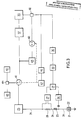
- Figure 3 shows a circuit which includes a normal configuration and a default configuration. The normal configuration corresponds to an AGC circuit substantially as shown in Figure 2. The distress configuration is adopted when the control tone falls below a threshold level.
- Loss of control tone is usually caused by a break in the cable and this prevents normal operation. The default mode is primarily intended for diagnostic tests. In particular the default mode indicates a failure at a particular location or plurality of locations in a long cable. This gives at least an approximate location of a fault.
- The circuit shown in Figure 3 includes four sub-circuits, namely:
- This is slightly modified from the AGC shown in Figure 2. Elements which perform similar functions have the same numeral.
- This sub-circuit detects the absence of control tone (or a signal proportional to the control tone). It holds the circuit in the normal configuration when the control tone is above a threshold value and it selects the default configuration when the control tone is below the threshold value. The selector includes switches to make the selection.
- This sub-circuit, which is part of the default configuration, enables the optical amplifier 20 to remain functional when there is no control tone and it provides a characteristic frequency to identify itself.
- This sub-circuit, which is also part of the default configuration, guards against unstable or overloaded operation when there is no control tone. It is desirable to protect against overload when starting operation (for the first time or after a break) or when operating in default mode for diagnostic purposes.
- The four sub-circuits will now be described separately.
- Item (1) above, ie the AGC, is shown in slightly more detail than in Figure 2. The extra elements are a
band pass filter 35 to separate control tone from other frequencies and arectifier 36 to provide a DC signal tocomparitor 30. The output of thecomparitor 30 is connected to anintegrator 37. In the normal configuration the output of theintegrator 37 is connected to the control port ofdevice 23 via two-way switch 41. - Item (2) above, ie the selector, comprises a
DC level sensor 46 which monitors the output ofrectifier 36 and acontrol device 47 to actuateswitches - Item 3 comprises a
resistive network 42 which produces a DC bias to substitute for the control signal whenever the AGC is rendered inoperative by the absence of control tone. The distress caller also includes alocal oscillator 43 to provide a distress tone characteristic of its own repeater, ie the distress tone is different at every repeater in the system.Oscillator 43 andresistive network 42 are connected to anadder 44 which combines the two signals. The combined signal passes to switch 41 which, in the default configuration, disconnects the AGC fromdevice 23 and connects theadder 44 todevice 23. - In the default configuration, ie in the absence of control tone, the
amplifier 26 and therefore themultiplier 29, will have zero input. Thecomparitor 30 will thus receive a zero input and in consequence it will produce a very high output in an attempt to achieve an impossible balance. The overload could be enough to damage itself and subsequent elements, ie theintegrator 37. In the default configuration, theamplifier 45 feeds back signal from the output of theintegrator 37 to the input of the comparitor 30 with a gain of, for example, 45dB. This provides a realistic input signal to thecomparitor 30 so that the loop 30-37-45-40-48 stabilises at a safe power. (Theadder 48 prevents detection of the loop signal by sensor 46). - In the normal configuration, the
detector 46 actuatescontrol unit 47 to disconnect the distress caller (42, 43, 44) and the overload guard sub-circuit (45, 40). The AGC operates as described above. The operation in the default mode will now be described. - The most usual accident is a broken cable. This clearly prevents all communication across the break. It is convenient to call the direction from land to the break "outward" and from the break to land "inward". Clearly there are two segments of cable, each with its own inward and outward direction.
- Electrical power to the amplifiers is provided via an electric conductor included in the optical cable. Even though the cable is broken it is still possible to provide an electrical supply. The sea is utilised as a return conductor but the broken end does not constitute a short circuit because the length and electrical resistance of even the broken segment will be substantial. Thus it is possible to retain the electrical power whereby the amplifier can still function.
- The cable is designed for two-directional communication and each segment will include both inward and outward telecommunications channels. Clearly the outward channels are useless even for diagnostics. The default mode operation of one inward channel will now be explained.
- The amplifier nearest the break will be designated "first" and its operation will be explained first. Even with the cable broken there is electric power and the amplifier 20 receives a drive current via
line 24 but there are no optical signals received at theinput facet 21 because of the break. Under these conditions the amplifier will act as an LED so there is an optical signal at theoutput facet 22. The mean power of the signal is set by the control from thenetwork 42, the conditions may not be optimal but they are at least useful. The local oscillator imposes its own characteristic distress ripple onto the drive current inline 24 and the optical output of theamplifier 22 is thereby amplitude modulated at this characteristic distress frequency. - The modulated LED signal is passed along a fibre to the next amplifier. There is no control tone so it takes the default configuration. It is still operational so that it amplifies its received signal and imposes its own characteristic distress frequency from its own local oscillator. Thus the optical signal produced at the
output facet 22 of the second amplifier is modulated with two distress frequencies. - The optical signal passes from amplifier to amplifier whereby, when it reaches land, it is modulated with the distress frequency of every amplifier in the chain. At the land station the optical signal is demodulated to an electrical signal with a complex wave form. This signal is fed to a frequency analyser which identifies the distress frequencies present. The presence of a particular distress frequency indicates that its amplifier is not only operative in the distress mode but also that it is connected to shore and hence the length of the broken segment can be deduced. Most cables comprise a plurality of inward channels and the diagnostic tests described can be repeated for each channel. This gives a plurality of results which, ideally, confirm one another.
- In addition the diagnostic tests can be performed on both segments of the cable. This may enable receipt of a distress frequency from every repeater, some at one end of the cable and the remainder at the other. This gives a very clear indication of the location of the break.
- If one segment were very long it might not be possible to provide electrical power to the outer end without overloading the inner end. In this case the other segment would be short and it would be possible to conduct the diagnostic tests but on the shorter length only.
- The overload guard sub-circuit not only protects the
comparitor 30 andintegrator 37 during default mode operation for diagnotic tests as described above but it also provides a desirable safeguard during the (transient) period when the cable is switched on. This applies at the very first switching on and whenever the cable is switched on after a break in operation, eg after an accident. - Consider the circuit shown in Figure 2. Under electric power and in the absence of optical signal, the comparitor 30 risks an overload. As shown in Figure 3, the default configuration is adopted and this includes protection against overload.
- If an optical signal, with control tone, is provided to the input facet of Figure 2, then, in the absence of electric power, there is no amplification and the circuit is dead. If power is switched on with signal present there is no amplification until a suitable drive current is established in
line 24. Furthermore, there will be no adequate signals to theamplifiers line 24. - Hence there is a transient period during which the
comparitor 30 and hencedevice 23 are without proper control signals. This is an unstable condition with a potential to overload. The modification shown in Figure 3 protects against this condition. When, because normal conditions have not yet been attained, there is a low control signal, thelevel sensor 46 actuatescontrol unit 47 to keep the circuit in the default configuration. Thus constantcurrent device 23 has an adequate control signal fromnetwork 42 whilecomparitor 30 andintegrator 37 are protected byamplifier 45. These are stable and safe conditions for optical amplifier 20 to establish its function.Level detector 46 reacts when the control signal fromrectifier 36 becomes adequate and it actuatescontrol unit 47 to invertswitches - It should be noted that
level sensor 46 is actuated by control tone (if present) in both the normal and default configurations. Thus the circuit switches to default configuration when control tone drops below the threshold value and it reverts to normal configuration when the control tone comes back to values above the threshold. - In normal operation the control tone is substantially constant after amplification. In default it is zero (or only noise). Therefore the precise setting of the threshold value is not important. Settings in the
range 25% to 75% of the normal value are suitable.
Claims (10)
(a) a laser amplifier for amplifying said optical signals;
(b) drive means for supplying drive current to the laser amplifier;
(c) a drive circuit connecting the drive means to the laser amplifier;
(d) AGC means connected to receive input from the drive circuit and having an output connected to control the drive current;
wherein the laser amplifier is adapted to superimpose an electrical control tone onto signals in the drive circuit, said electrical control tone being derived from received optical control tone, and said AGC means is adapted to produce a parameter signal from said electrical control tone and to vary the drive current so as to keep the control parameter at a pre-set level.
(i) a normal configuration;
(ii) a default configuration; and
(iii) selector means operative to select between configurations (i) and (ii);
W wherein configuration (i) comprises:-
(a) a laser amplifier for amplifying said optical signals;
(b) drive means for supplying drive current to the laser amplifier;
(c) a drive circuit connecting the drive means to the laser amplifier;
(d) AGC means connected to receive input from the drive circuit and having an output connected to control the drive current;
wherein the laser amplifier is adapted to superimpose an electrical control tone onto signals in the drive circuit, said electrical control tone being derived from received optical control tone, and said AGC means is adapted to produce a parameter signal from said electrical control tone and to vary the drive current so as to keep the control parameter at a pre-set level; configuration (ii) comprises alternate means for providing drive current to said laser amplifier and the selector means includes a detector responsive to a level of control tone below a threshold level and switching means operatively linked to said detector means, said switching means being adapted to connect the normal configuration when the detected level is above the threshold and to connect the default configuration when the detected level is below the threshold.
Priority Applications (1)
| Application Number | Priority Date | Filing Date | Title |
|---|---|---|---|
| AT89301356T ATE97771T1 (en) | 1988-03-04 | 1989-02-13 | AMPLIFICATION OF OPTICAL SIGNALS. |
Applications Claiming Priority (4)
| Application Number | Priority Date | Filing Date | Title |
|---|---|---|---|
| GB8805204 | 1988-03-04 | ||
| GB888805204A GB8805204D0 (en) | 1988-03-04 | 1988-03-04 | Amplification of optical signals |
| GB888818107A GB8818107D0 (en) | 1988-07-29 | 1988-07-29 | Amplification of optical signals |
| GB8818107 | 1988-07-29 |
Publications (3)
| Publication Number | Publication Date |
|---|---|
| EP0331304A2 true EP0331304A2 (en) | 1989-09-06 |
| EP0331304A3 EP0331304A3 (en) | 1989-12-20 |
| EP0331304B1 EP0331304B1 (en) | 1993-11-24 |
Family
ID=26293583
Family Applications (1)
| Application Number | Title | Priority Date | Filing Date |
|---|---|---|---|
| EP89301356A Expired - Lifetime EP0331304B1 (en) | 1988-03-04 | 1989-02-13 | Amplification of optical signals |
Country Status (5)
| Country | Link |
|---|---|
| US (1) | US4995100A (en) |
| EP (1) | EP0331304B1 (en) |
| JP (2) | JP2963103B2 (en) |
| CA (1) | CA1293996C (en) |
| DE (1) | DE68910851T2 (en) |
Cited By (9)
| Publication number | Priority date | Publication date | Assignee | Title |
|---|---|---|---|---|
| FR2663480A1 (en) * | 1990-06-16 | 1991-12-20 | Northern Telecom Ltd | METHOD AND APPARATUS FOR ANALOGUE TELEMETRY FOR OPTICAL TRANSMISSION SYSTEM. |
| FR2663481A1 (en) * | 1990-06-16 | 1991-12-20 | Northern Telecom Ltd | METHOD AND INSTALLATION OF DIGITAL TELEMETRY |
| EP0506163A1 (en) * | 1991-03-29 | 1992-09-30 | PIRELLI CAVI S.p.A. | Optical-fibre telecommunications line with protection device for optical amplifiers |
| WO1992017008A1 (en) * | 1991-03-22 | 1992-10-01 | British Telecommunications Public Limited Company | Photonic amplifier |
| WO1993002344A1 (en) * | 1991-07-18 | 1993-02-04 | British Telecommunications Public Limited Company | Fault location in optical systems |
| EP0580316A1 (en) * | 1992-07-17 | 1994-01-26 | AT&T Corp. | Performance monitoring and fault location for optical equipment, systems and networks |
| US5355250A (en) * | 1991-03-29 | 1994-10-11 | Pirelli Cavi S.P.A. | Fiber optical communication line with shut off control |
| US5475385A (en) * | 1990-06-16 | 1995-12-12 | Northern Telecom Limited | Analogue telemetry system and method for fault detection in optical transmission systems |
| EP0703678A3 (en) * | 1994-08-25 | 1997-04-16 | At & T Corp | Performance monitoring and fault location in optical transmission systems |
Families Citing this family (10)
| Publication number | Priority date | Publication date | Assignee | Title |
|---|---|---|---|---|
| GB9008895D0 (en) * | 1990-04-20 | 1990-06-20 | British Telecomm | Optical communications link fault signalling |
| JPH04217123A (en) * | 1990-12-18 | 1992-08-07 | Fujitsu Ltd | Feeding system for optical transmission system |
| DE4106778A1 (en) * | 1991-03-04 | 1992-09-10 | Standard Elektrik Lorenz Ag | OPTICAL-ELECTRIC CONVERTER WITH EXTENDED DYNAMICS |
| US5268786A (en) * | 1991-03-15 | 1993-12-07 | Mitsubishi Denki Kabushiki Kaisha | Optical fiber amplifier and its amplification method |
| US5513029A (en) * | 1994-06-16 | 1996-04-30 | Northern Telecom Limited | Method and apparatus for monitoring performance of optical transmission systems |
| US5563731A (en) * | 1995-02-22 | 1996-10-08 | Nec Corporation | Monitor control signal receiving apparatus for optical fiber amplifier |
| JP4204693B2 (en) | 1999-03-31 | 2009-01-07 | 三菱電機株式会社 | Optical amplifier |
| JP2002198598A (en) * | 2000-12-22 | 2002-07-12 | Nec Corp | Circuit and method for optical amplification gain control |
| US7215891B1 (en) | 2003-06-06 | 2007-05-08 | Jds Uniphase Corporation | Integrated driving, receiving, controlling, and monitoring for optical transceivers |
| US8036539B2 (en) * | 2005-06-28 | 2011-10-11 | Finisar Corporation | Gigabit ethernet longwave optical transceiver module having amplified bias current |
Citations (5)
| Publication number | Priority date | Publication date | Assignee | Title |
|---|---|---|---|---|
| GB2025121A (en) * | 1978-07-06 | 1980-01-16 | Post Office | Improvements in or relating to the stabilisation of injection lasers |
| US4257033A (en) * | 1978-08-07 | 1981-03-17 | Kokusai Denshin Denwa Kabushiki Kaisha | Fault locating system in optical fiber transmission system |
| FR2524230A1 (en) * | 1982-03-26 | 1983-09-30 | Lignes Telegraph Telephon | Information transmission system for optical fibre link - uses generator to modulate information signal with service signals, and low pass filter to maintain constant output of laser diode |
| JPS5986930A (en) * | 1982-11-11 | 1984-05-19 | Fujitsu Ltd | Optical repeater |
| JPS61262327A (en) * | 1985-05-16 | 1986-11-20 | Mitsubishi Electric Corp | Analog modulation circuit of laser diode |
Family Cites Families (6)
| Publication number | Priority date | Publication date | Assignee | Title |
|---|---|---|---|---|
| JPS4991784A (en) * | 1973-01-05 | 1974-09-02 | ||
| US4574249A (en) * | 1981-09-08 | 1986-03-04 | At&T Bell Laboratories | Nonintegrating lightwave receiver |
| US4499610A (en) * | 1983-06-30 | 1985-02-12 | Gould Inc. | Feedback system with automatic gain control action |
| JPS59145586A (en) * | 1983-12-27 | 1984-08-21 | Sumitomo Electric Ind Ltd | Direct current bias circuit for semiconductor laser |
| US4688268A (en) * | 1984-01-11 | 1987-08-18 | Chevron Research Company | Fiber optic receiver having a combined baseline clamp and automatic gain control detector |
| US4859015A (en) * | 1988-08-17 | 1989-08-22 | The Boeing Company | Optical receiver having optical gain medium and mode selector |
-
1989
- 1989-02-13 DE DE89301356T patent/DE68910851T2/en not_active Expired - Fee Related
- 1989-02-13 EP EP89301356A patent/EP0331304B1/en not_active Expired - Lifetime
- 1989-03-02 US US07/318,221 patent/US4995100A/en not_active Expired - Lifetime
- 1989-03-03 JP JP1051803A patent/JP2963103B2/en not_active Expired - Fee Related
- 1989-03-06 CA CA000592790A patent/CA1293996C/en not_active Expired - Lifetime
-
1999
- 1999-04-12 JP JP11104196A patent/JP3078535B2/en not_active Expired - Lifetime
Patent Citations (5)
| Publication number | Priority date | Publication date | Assignee | Title |
|---|---|---|---|---|
| GB2025121A (en) * | 1978-07-06 | 1980-01-16 | Post Office | Improvements in or relating to the stabilisation of injection lasers |
| US4257033A (en) * | 1978-08-07 | 1981-03-17 | Kokusai Denshin Denwa Kabushiki Kaisha | Fault locating system in optical fiber transmission system |
| FR2524230A1 (en) * | 1982-03-26 | 1983-09-30 | Lignes Telegraph Telephon | Information transmission system for optical fibre link - uses generator to modulate information signal with service signals, and low pass filter to maintain constant output of laser diode |
| JPS5986930A (en) * | 1982-11-11 | 1984-05-19 | Fujitsu Ltd | Optical repeater |
| JPS61262327A (en) * | 1985-05-16 | 1986-11-20 | Mitsubishi Electric Corp | Analog modulation circuit of laser diode |
Non-Patent Citations (3)
| Title |
|---|
| IEEE Int. Conf. on Communications, ICC-85, Chicago, June 23-26, 1985, Conf. Rec. Vol. 3 of 3, pages 1035-1039; IEEE, New York, US, Y. NIIRO: "The OS-280M system for long-haul optical fiber submarine cable communications". * |
| PATENT ABSTRACTS OF JAPAN, Vol. 11, No. 113 (E-497)(2560), April 9, 1987; & JP-A-61 262 327 (MITSUBISHI ELECTRIC CORP.) 20-11-1986 * |
| PATENT ABSTRACTS OF JAPAN, Vol. 8, No. 198 (E-265)(1635), September 11, 1984; & JP-A-59 086 930 (FUJITSU K.K.) 19-05-1984 * |
Cited By (16)
| Publication number | Priority date | Publication date | Assignee | Title |
|---|---|---|---|---|
| US5475385A (en) * | 1990-06-16 | 1995-12-12 | Northern Telecom Limited | Analogue telemetry system and method for fault detection in optical transmission systems |
| FR2663481A1 (en) * | 1990-06-16 | 1991-12-20 | Northern Telecom Ltd | METHOD AND INSTALLATION OF DIGITAL TELEMETRY |
| FR2664450A1 (en) * | 1990-06-16 | 1992-01-10 | Northern Telecom Ltd | METHOD AND INSTALLATION OF ANALOGUE TELEMETRY. |
| US5483233A (en) * | 1990-06-16 | 1996-01-09 | Northern Telecom Limited | Analogue telemetry system and method for fault detection in optical transmission systems |
| US5260819A (en) * | 1990-06-16 | 1993-11-09 | Northern Telecom Limited | Digital telemetry system and method for fault detection in optical transmission system |
| FR2663480A1 (en) * | 1990-06-16 | 1991-12-20 | Northern Telecom Ltd | METHOD AND APPARATUS FOR ANALOGUE TELEMETRY FOR OPTICAL TRANSMISSION SYSTEM. |
| WO1992017008A1 (en) * | 1991-03-22 | 1992-10-01 | British Telecommunications Public Limited Company | Photonic amplifier |
| AU661298B2 (en) * | 1991-03-22 | 1995-07-20 | Ipg Photonics Corporation | Photonic amplifier |
| EP0506163A1 (en) * | 1991-03-29 | 1992-09-30 | PIRELLI CAVI S.p.A. | Optical-fibre telecommunications line with protection device for optical amplifiers |
| US5278686A (en) * | 1991-03-29 | 1994-01-11 | Pirelli Cavi S.P.A. | Optical-fibre telecommunications line with protection device for optical amplifiers |
| US5355250A (en) * | 1991-03-29 | 1994-10-11 | Pirelli Cavi S.P.A. | Fiber optical communication line with shut off control |
| AU665205B2 (en) * | 1991-07-18 | 1995-12-21 | British Telecommunications Public Limited Company | Fault location in optical systems |
| WO1993002344A1 (en) * | 1991-07-18 | 1993-02-04 | British Telecommunications Public Limited Company | Fault location in optical systems |
| US5528404A (en) * | 1991-07-18 | 1996-06-18 | British Telecommunications Public Limited Company | Fault location in optical systems |
| EP0580316A1 (en) * | 1992-07-17 | 1994-01-26 | AT&T Corp. | Performance monitoring and fault location for optical equipment, systems and networks |
| EP0703678A3 (en) * | 1994-08-25 | 1997-04-16 | At & T Corp | Performance monitoring and fault location in optical transmission systems |
Also Published As
| Publication number | Publication date |
|---|---|
| JP3078535B2 (en) | 2000-08-21 |
| CA1293996C (en) | 1992-01-07 |
| EP0331304B1 (en) | 1993-11-24 |
| JP2000049711A (en) | 2000-02-18 |
| DE68910851T2 (en) | 1994-05-05 |
| US4995100A (en) | 1991-02-19 |
| DE68910851D1 (en) | 1994-01-05 |
| EP0331304A3 (en) | 1989-12-20 |
| JPH0269982A (en) | 1990-03-08 |
| JP2963103B2 (en) | 1999-10-12 |
Similar Documents
| Publication | Publication Date | Title |
|---|---|---|
| EP0331304B1 (en) | Amplification of optical signals | |
| US6067187A (en) | Optical amplifier and optical communication system employing the same | |
| US5703711A (en) | In-line optical amplifier | |
| US6288836B1 (en) | Optical amplifier and optical communication system having the optical amplifier | |
| JP2723067B2 (en) | Optical amplifier | |
| US6859308B2 (en) | Optical amplifier | |
| US5296957A (en) | Optical repeater having loop-back function used in transmission system | |
| US5920414A (en) | Wavelength division multiplexing optical transmission apparatus and optical repeater | |
| JPH04502211A (en) | Optical fiber link noise measurement and optimization system | |
| EP0910182A2 (en) | Optical transmission device and optical communication system | |
| JPH0895097A (en) | Wave-length multiplexing optical amplifier | |
| JPH07112173B2 (en) | Light modulation circuit | |
| JPH08265258A (en) | Light amplification repeater | |
| EP0784391A2 (en) | Wavelength division multiplexing light transmitting system | |
| US7554720B2 (en) | Optical transmission apparatus with automatic gain control and automatic level control mode selection | |
| EP0904641B1 (en) | Fibre optic transmission with fibre amplifiers and supervisory signals | |
| US8401397B2 (en) | Optical reception device, optical receiving method, and optical transmission apparatus | |
| JP4084144B2 (en) | Optical amplifier | |
| US7062169B2 (en) | Systems and methods for compensating for signal transients | |
| JPH0468830A (en) | Light amplifying repeater | |
| US6169615B1 (en) | Wavelength division multiplex optical transmission apparatus | |
| CA2118449A1 (en) | Method and system for indicating an optical transmit amplifier fault | |
| JPH05292033A (en) | Monitor control system for optical transmission line | |
| US20040202469A1 (en) | Method of controlling optical wavelength division multiplexing transmission apparatus | |
| JPH11225115A (en) | Wavelength multiplex transmission system |
Legal Events
| Date | Code | Title | Description |
|---|---|---|---|
| PUAI | Public reference made under article 153(3) epc to a published international application that has entered the european phase |
Free format text: ORIGINAL CODE: 0009012 |
|
| AK | Designated contracting states |
Kind code of ref document: A2 Designated state(s): AT BE CH DE ES FR GB GR IT LI LU NL SE |
|
| PUAL | Search report despatched |
Free format text: ORIGINAL CODE: 0009013 |
|
| AK | Designated contracting states |
Kind code of ref document: A3 Designated state(s): AT BE CH DE ES FR GB GR IT LI LU NL SE |
|
| 17P | Request for examination filed |
Effective date: 19900131 |
|
| 17Q | First examination report despatched |
Effective date: 19920402 |
|
| GRAA | (expected) grant |
Free format text: ORIGINAL CODE: 0009210 |
|
| AK | Designated contracting states |
Kind code of ref document: B1 Designated state(s): AT BE CH DE ES FR GB GR IT LI LU NL SE |
|
| PG25 | Lapsed in a contracting state [announced via postgrant information from national office to epo] |
Ref country code: SE Effective date: 19931124 Ref country code: LI Effective date: 19931124 Ref country code: GR Free format text: LAPSE BECAUSE OF FAILURE TO SUBMIT A TRANSLATION OF THE DESCRIPTION OR TO PAY THE FEE WITHIN THE PRESCRIBED TIME-LIMIT Effective date: 19931124 Ref country code: ES Free format text: THE PATENT HAS BEEN ANNULLED BY A DECISION OF A NATIONAL AUTHORITY Effective date: 19931124 Ref country code: CH Effective date: 19931124 Ref country code: BE Effective date: 19931124 Ref country code: AT Effective date: 19931124 |
|
| REF | Corresponds to: |
Ref document number: 97771 Country of ref document: AT Date of ref document: 19931215 Kind code of ref document: T |
|
| ITF | It: translation for a ep patent filed |
Owner name: JACOBACCI CASETTA & PERANI S.P.A. |
|
| REF | Corresponds to: |
Ref document number: 68910851 Country of ref document: DE Date of ref document: 19940105 |
|
| PG25 | Lapsed in a contracting state [announced via postgrant information from national office to epo] |
Ref country code: LU Free format text: LAPSE BECAUSE OF NON-PAYMENT OF DUE FEES Effective date: 19940228 |
|
| REG | Reference to a national code |
Ref country code: CH Ref legal event code: PL |
|
| ET | Fr: translation filed | ||
| PLBE | No opposition filed within time limit |
Free format text: ORIGINAL CODE: 0009261 |
|
| STAA | Information on the status of an ep patent application or granted ep patent |
Free format text: STATUS: NO OPPOSITION FILED WITHIN TIME LIMIT |
|
| 26N | No opposition filed | ||
| PGFP | Annual fee paid to national office [announced via postgrant information from national office to epo] |
Ref country code: NL Payment date: 20000117 Year of fee payment: 12 |
|
| REG | Reference to a national code |
Ref country code: GB Ref legal event code: 732E |
|
| PG25 | Lapsed in a contracting state [announced via postgrant information from national office to epo] |
Ref country code: NL Free format text: LAPSE BECAUSE OF NON-PAYMENT OF DUE FEES Effective date: 20010901 |
|
| NLV4 | Nl: lapsed or anulled due to non-payment of the annual fee |
Effective date: 20010901 |
|
| REG | Reference to a national code |
Ref country code: GB Ref legal event code: IF02 |
|
| PGFP | Annual fee paid to national office [announced via postgrant information from national office to epo] |
Ref country code: FR Payment date: 20020114 Year of fee payment: 14 |
|
| PGFP | Annual fee paid to national office [announced via postgrant information from national office to epo] |
Ref country code: GB Payment date: 20020117 Year of fee payment: 14 |
|
| PGFP | Annual fee paid to national office [announced via postgrant information from national office to epo] |
Ref country code: DE Payment date: 20020121 Year of fee payment: 14 |
|
| PG25 | Lapsed in a contracting state [announced via postgrant information from national office to epo] |
Ref country code: GB Free format text: LAPSE BECAUSE OF NON-PAYMENT OF DUE FEES Effective date: 20030213 |
|
| PG25 | Lapsed in a contracting state [announced via postgrant information from national office to epo] |
Ref country code: DE Free format text: LAPSE BECAUSE OF NON-PAYMENT OF DUE FEES Effective date: 20030902 |
|
| GBPC | Gb: european patent ceased through non-payment of renewal fee | ||
| PG25 | Lapsed in a contracting state [announced via postgrant information from national office to epo] |
Ref country code: FR Free format text: LAPSE BECAUSE OF NON-PAYMENT OF DUE FEES Effective date: 20031031 |
|
| REG | Reference to a national code |
Ref country code: FR Ref legal event code: ST |
|
| PG25 | Lapsed in a contracting state [announced via postgrant information from national office to epo] |
Ref country code: IT Free format text: LAPSE BECAUSE OF NON-PAYMENT OF DUE FEES;WARNING: LAPSES OF ITALIAN PATENTS WITH EFFECTIVE DATE BEFORE 2007 MAY HAVE OCCURRED AT ANY TIME BEFORE 2007. THE CORRECT EFFECTIVE DATE MAY BE DIFFERENT FROM THE ONE RECORDED. Effective date: 20050213 |