EP0330395A2 - Switching element - Google Patents
Switching element Download PDFInfo
- Publication number
- EP0330395A2 EP0330395A2 EP89301600A EP89301600A EP0330395A2 EP 0330395 A2 EP0330395 A2 EP 0330395A2 EP 89301600 A EP89301600 A EP 89301600A EP 89301600 A EP89301600 A EP 89301600A EP 0330395 A2 EP0330395 A2 EP 0330395A2
- Authority
- EP
- European Patent Office
- Prior art keywords
- switching element
- film
- element according
- electrodes
- region
- Prior art date
- Legal status (The legal status is an assumption and is not a legal conclusion. Google has not performed a legal analysis and makes no representation as to the accuracy of the status listed.)
- Granted
Links
- 239000010408 film Substances 0.000 claims description 70
- 238000000034 method Methods 0.000 claims description 57
- 239000010409 thin film Substances 0.000 claims description 11
- 239000011368 organic material Substances 0.000 claims description 7
- 239000000758 substrate Substances 0.000 description 34
- 230000003287 optical effect Effects 0.000 description 19
- 239000010410 layer Substances 0.000 description 18
- XLYOFNOQVPJJNP-UHFFFAOYSA-N water Substances O XLYOFNOQVPJJNP-UHFFFAOYSA-N 0.000 description 16
- 238000006243 chemical reaction Methods 0.000 description 13
- 239000000463 material Substances 0.000 description 11
- UHOVQNZJYSORNB-UHFFFAOYSA-N Benzene Chemical compound C1=CC=CC=C1 UHOVQNZJYSORNB-UHFFFAOYSA-N 0.000 description 9
- 239000004642 Polyimide Substances 0.000 description 9
- 230000002209 hydrophobic effect Effects 0.000 description 9
- 150000002894 organic compounds Chemical class 0.000 description 9
- 229920001721 polyimide Polymers 0.000 description 9
- 230000015572 biosynthetic process Effects 0.000 description 7
- 230000008569 process Effects 0.000 description 6
- 239000004065 semiconductor Substances 0.000 description 6
- 150000001875 compounds Chemical class 0.000 description 5
- 239000000975 dye Substances 0.000 description 5
- 239000000243 solution Substances 0.000 description 5
- 238000007740 vapor deposition Methods 0.000 description 5
- 239000002253 acid Substances 0.000 description 4
- 229920001577 copolymer Polymers 0.000 description 4
- 238000010586 diagram Methods 0.000 description 4
- 229910052751 metal Inorganic materials 0.000 description 4
- 239000002184 metal Substances 0.000 description 4
- 229920000642 polymer Polymers 0.000 description 4
- VZCYOOQTPOCHFL-UHFFFAOYSA-N trans-butenedioic acid Natural products OC(=O)C=CC(O)=O VZCYOOQTPOCHFL-UHFFFAOYSA-N 0.000 description 4
- WFDIJRYMOXRFFG-UHFFFAOYSA-N Acetic anhydride Chemical compound CC(=O)OC(C)=O WFDIJRYMOXRFFG-UHFFFAOYSA-N 0.000 description 3
- WEVYAHXRMPXWCK-UHFFFAOYSA-N Acetonitrile Chemical compound CC#N WEVYAHXRMPXWCK-UHFFFAOYSA-N 0.000 description 3
- 229910001218 Gallium arsenide Inorganic materials 0.000 description 3
- REYJJPSVUYRZGE-UHFFFAOYSA-N Octadecylamine Chemical class CCCCCCCCCCCCCCCCCCN REYJJPSVUYRZGE-UHFFFAOYSA-N 0.000 description 3
- 239000004952 Polyamide Substances 0.000 description 3
- 230000002776 aggregation Effects 0.000 description 3
- 238000004220 aggregation Methods 0.000 description 3
- 229910021417 amorphous silicon Inorganic materials 0.000 description 3
- 230000001276 controlling effect Effects 0.000 description 3
- 238000011161 development Methods 0.000 description 3
- 230000000694 effects Effects 0.000 description 3
- 230000001747 exhibiting effect Effects 0.000 description 3
- 239000011521 glass Substances 0.000 description 3
- 238000005192 partition Methods 0.000 description 3
- 229920002647 polyamide Polymers 0.000 description 3
- 230000005855 radiation Effects 0.000 description 3
- 239000002904 solvent Substances 0.000 description 3
- HEDRZPFGACZZDS-UHFFFAOYSA-N Chloroform Chemical compound ClC(Cl)Cl HEDRZPFGACZZDS-UHFFFAOYSA-N 0.000 description 2
- VZCYOOQTPOCHFL-OWOJBTEDSA-N Fumaric acid Natural products OC(=O)\C=C\C(O)=O VZCYOOQTPOCHFL-OWOJBTEDSA-N 0.000 description 2
- KDLHZDBZIXYQEI-UHFFFAOYSA-N Palladium Chemical compound [Pd] KDLHZDBZIXYQEI-UHFFFAOYSA-N 0.000 description 2
- OFOBLEOULBTSOW-UHFFFAOYSA-N Propanedioic acid Natural products OC(=O)CC(O)=O OFOBLEOULBTSOW-UHFFFAOYSA-N 0.000 description 2
- JUJWROOIHBZHMG-UHFFFAOYSA-N Pyridine Chemical compound C1=CC=NC=C1 JUJWROOIHBZHMG-UHFFFAOYSA-N 0.000 description 2
- SMWDFEZZVXVKRB-UHFFFAOYSA-N Quinoline Chemical compound N1=CC=CC2=CC=CC=C21 SMWDFEZZVXVKRB-UHFFFAOYSA-N 0.000 description 2
- VYPSYNLAJGMNEJ-UHFFFAOYSA-N Silicium dioxide Chemical compound O=[Si]=O VYPSYNLAJGMNEJ-UHFFFAOYSA-N 0.000 description 2
- 229920002125 Sokalan® Polymers 0.000 description 2
- 125000000217 alkyl group Chemical group 0.000 description 2
- 229910052782 aluminium Inorganic materials 0.000 description 2
- MWPLVEDNUUSJAV-UHFFFAOYSA-N anthracene Chemical compound C1=CC=CC2=CC3=CC=CC=C3C=C21 MWPLVEDNUUSJAV-UHFFFAOYSA-N 0.000 description 2
- CUFNKYGDVFVPHO-UHFFFAOYSA-N azulene Chemical compound C1=CC=CC2=CC=CC2=C1 CUFNKYGDVFVPHO-UHFFFAOYSA-N 0.000 description 2
- IOJUPLGTWVMSFF-UHFFFAOYSA-N benzothiazole Chemical compound C1=CC=C2SC=NC2=C1 IOJUPLGTWVMSFF-UHFFFAOYSA-N 0.000 description 2
- 239000011247 coating layer Substances 0.000 description 2
- 230000003247 decreasing effect Effects 0.000 description 2
- 229910052731 fluorine Chemical group 0.000 description 2
- 239000011737 fluorine Chemical group 0.000 description 2
- 125000001153 fluoro group Chemical group F* 0.000 description 2
- 239000001530 fumaric acid Substances 0.000 description 2
- 230000006870 function Effects 0.000 description 2
- 239000007789 gas Substances 0.000 description 2
- 125000001165 hydrophobic group Chemical group 0.000 description 2
- 238000007654 immersion Methods 0.000 description 2
- 238000003475 lamination Methods 0.000 description 2
- 239000011976 maleic acid Substances 0.000 description 2
- 150000002739 metals Chemical class 0.000 description 2
- 125000001434 methanylylidene group Chemical group [H]C#[*] 0.000 description 2
- IEQIEDJGQAUEQZ-UHFFFAOYSA-N phthalocyanine Chemical compound N1C(N=C2C3=CC=CC=C3C(N=C3C4=CC=CC=C4C(=N4)N3)=N2)=C(C=CC=C2)C2=C1N=C1C2=CC=CC=C2C4=N1 IEQIEDJGQAUEQZ-UHFFFAOYSA-N 0.000 description 2
- -1 polycyclic aromatic compounds Chemical class 0.000 description 2
- BBEAQIROQSPTKN-UHFFFAOYSA-N pyrene Chemical compound C1=CC=C2C=CC3=CC=CC4=CC=C1C2=C43 BBEAQIROQSPTKN-UHFFFAOYSA-N 0.000 description 2
- 150000003839 salts Chemical class 0.000 description 2
- 229910021332 silicide Inorganic materials 0.000 description 2
- 229910052710 silicon Inorganic materials 0.000 description 2
- 239000007787 solid Substances 0.000 description 2
- 238000004544 sputter deposition Methods 0.000 description 2
- 239000000126 substance Substances 0.000 description 2
- 238000006467 substitution reaction Methods 0.000 description 2
- 238000012546 transfer Methods 0.000 description 2
- 230000007704 transition Effects 0.000 description 2
- 238000001771 vacuum deposition Methods 0.000 description 2
- QGKMIGUHVLGJBR-UHFFFAOYSA-M (4z)-1-(3-methylbutyl)-4-[[1-(3-methylbutyl)quinolin-1-ium-4-yl]methylidene]quinoline;iodide Chemical compound [I-].C12=CC=CC=C2N(CCC(C)C)C=CC1=CC1=CC=[N+](CCC(C)C)C2=CC=CC=C12 QGKMIGUHVLGJBR-UHFFFAOYSA-M 0.000 description 1
- BCMCBBGGLRIHSE-UHFFFAOYSA-N 1,3-benzoxazole Chemical compound C1=CC=C2OC=NC2=C1 BCMCBBGGLRIHSE-UHFFFAOYSA-N 0.000 description 1
- CMSGUKVDXXTJDQ-UHFFFAOYSA-N 4-(2-naphthalen-1-ylethylamino)-4-oxobutanoic acid Chemical compound C1=CC=C2C(CCNC(=O)CCC(=O)O)=CC=CC2=C1 CMSGUKVDXXTJDQ-UHFFFAOYSA-N 0.000 description 1
- 229920002126 Acrylic acid copolymer Polymers 0.000 description 1
- OKTJSMMVPCPJKN-UHFFFAOYSA-N Carbon Chemical compound [C] OKTJSMMVPCPJKN-UHFFFAOYSA-N 0.000 description 1
- 102000018832 Cytochromes Human genes 0.000 description 1
- 108010052832 Cytochromes Proteins 0.000 description 1
- FXHOOIRPVKKKFG-UHFFFAOYSA-N N,N-Dimethylacetamide Chemical compound CN(C)C(C)=O FXHOOIRPVKKKFG-UHFFFAOYSA-N 0.000 description 1
- DFPAKSUCGFBDDF-UHFFFAOYSA-N Nicotinamide Chemical group NC(=O)C1=CC=CN=C1 DFPAKSUCGFBDDF-UHFFFAOYSA-N 0.000 description 1
- ABLZXFCXXLZCGV-UHFFFAOYSA-N Phosphorous acid Chemical compound OP(O)=O ABLZXFCXXLZCGV-UHFFFAOYSA-N 0.000 description 1
- 229910052581 Si3N4 Inorganic materials 0.000 description 1
- BLRPTPMANUNPDV-UHFFFAOYSA-N Silane Chemical compound [SiH4] BLRPTPMANUNPDV-UHFFFAOYSA-N 0.000 description 1
- XUIMIQQOPSSXEZ-UHFFFAOYSA-N Silicon Chemical compound [Si] XUIMIQQOPSSXEZ-UHFFFAOYSA-N 0.000 description 1
- 238000009825 accumulation Methods 0.000 description 1
- 229910045601 alloy Inorganic materials 0.000 description 1
- 239000000956 alloy Substances 0.000 description 1
- PNEYBMLMFCGWSK-UHFFFAOYSA-N aluminium oxide Inorganic materials [O-2].[O-2].[O-2].[Al+3].[Al+3] PNEYBMLMFCGWSK-UHFFFAOYSA-N 0.000 description 1
- 125000003277 amino group Chemical group 0.000 description 1
- 229910052980 cadmium sulfide Inorganic materials 0.000 description 1
- 125000003178 carboxy group Chemical group [H]OC(*)=O 0.000 description 1
- 150000007942 carboxylates Chemical class 0.000 description 1
- 150000001735 carboxylic acids Chemical class 0.000 description 1
- 230000008859 change Effects 0.000 description 1
- 229910052681 coesite Inorganic materials 0.000 description 1
- 238000009833 condensation Methods 0.000 description 1
- 230000005494 condensation Effects 0.000 description 1
- 239000004020 conductor Substances 0.000 description 1
- 229910052593 corundum Inorganic materials 0.000 description 1
- 229910052906 cristobalite Inorganic materials 0.000 description 1
- 230000001186 cumulative effect Effects 0.000 description 1
- 235000014113 dietary fatty acids Nutrition 0.000 description 1
- NAPSCFZYZVSQHF-UHFFFAOYSA-N dimantine Chemical compound CCCCCCCCCCCCCCCCCCN(C)C NAPSCFZYZVSQHF-UHFFFAOYSA-N 0.000 description 1
- 125000004185 ester group Chemical group 0.000 description 1
- 150000002148 esters Chemical class 0.000 description 1
- 239000000194 fatty acid Substances 0.000 description 1
- 229930195729 fatty acid Natural products 0.000 description 1
- 150000004665 fatty acids Chemical class 0.000 description 1
- GVEPBJHOBDJJJI-UHFFFAOYSA-N fluoranthrene Natural products C1=CC(C2=CC=CC=C22)=C3C2=CC=CC3=C1 GVEPBJHOBDJJJI-UHFFFAOYSA-N 0.000 description 1
- 229910052737 gold Inorganic materials 0.000 description 1
- 229910002804 graphite Inorganic materials 0.000 description 1
- 239000010439 graphite Substances 0.000 description 1
- 150000002391 heterocyclic compounds Chemical class 0.000 description 1
- 150000002430 hydrocarbons Chemical group 0.000 description 1
- 230000005660 hydrophilic surface Effects 0.000 description 1
- 125000002887 hydroxy group Chemical group [H]O* 0.000 description 1
- 238000006358 imidation reaction Methods 0.000 description 1
- 125000005462 imide group Chemical group 0.000 description 1
- PJXISJQVUVHSOJ-UHFFFAOYSA-N indium(III) oxide Inorganic materials [O-2].[O-2].[O-2].[In+3].[In+3] PJXISJQVUVHSOJ-UHFFFAOYSA-N 0.000 description 1
- 229910010272 inorganic material Inorganic materials 0.000 description 1
- 239000011147 inorganic material Substances 0.000 description 1
- 230000009878 intermolecular interaction Effects 0.000 description 1
- 229910052745 lead Inorganic materials 0.000 description 1
- 125000005647 linker group Chemical group 0.000 description 1
- 150000002678 macrocyclic compounds Chemical class 0.000 description 1
- 238000012423 maintenance Methods 0.000 description 1
- 238000005259 measurement Methods 0.000 description 1
- 230000006386 memory function Effects 0.000 description 1
- 239000011259 mixed solution Substances 0.000 description 1
- 239000012046 mixed solvent Substances 0.000 description 1
- 238000001451 molecular beam epitaxy Methods 0.000 description 1
- 239000000178 monomer Substances 0.000 description 1
- 229910052759 nickel Inorganic materials 0.000 description 1
- PXHVJJICTQNCMI-UHFFFAOYSA-N nickel Substances [Ni] PXHVJJICTQNCMI-UHFFFAOYSA-N 0.000 description 1
- 229910021334 nickel silicide Inorganic materials 0.000 description 1
- RUFLMLWJRZAWLJ-UHFFFAOYSA-N nickel silicide Chemical compound [Ni]=[Si]=[Ni] RUFLMLWJRZAWLJ-UHFFFAOYSA-N 0.000 description 1
- 150000004767 nitrides Chemical class 0.000 description 1
- 229910052763 palladium Inorganic materials 0.000 description 1
- 125000001997 phenyl group Chemical group [H]C1=C([H])C([H])=C(*)C([H])=C1[H] 0.000 description 1
- 125000002467 phosphate group Chemical group [H]OP(=O)(O[H])O[*] 0.000 description 1
- 230000000704 physical effect Effects 0.000 description 1
- 229910052697 platinum Inorganic materials 0.000 description 1
- 229920005575 poly(amic acid) Polymers 0.000 description 1
- 239000004584 polyacrylic acid Substances 0.000 description 1
- 229910021420 polycrystalline silicon Inorganic materials 0.000 description 1
- 125000003367 polycyclic group Chemical group 0.000 description 1
- 229920000015 polydiacetylene Polymers 0.000 description 1
- 239000002861 polymer material Substances 0.000 description 1
- 238000006116 polymerization reaction Methods 0.000 description 1
- 229920001184 polypeptide Polymers 0.000 description 1
- 229920005591 polysilicon Polymers 0.000 description 1
- 150000004032 porphyrins Chemical group 0.000 description 1
- 238000005036 potential barrier Methods 0.000 description 1
- 102000004196 processed proteins & peptides Human genes 0.000 description 1
- 108090000765 processed proteins & peptides Proteins 0.000 description 1
- UMJSCPRVCHMLSP-UHFFFAOYSA-N pyridine Natural products COC1=CC=CN=C1 UMJSCPRVCHMLSP-UHFFFAOYSA-N 0.000 description 1
- 239000011347 resin Substances 0.000 description 1
- 229920005989 resin Polymers 0.000 description 1
- 230000004044 response Effects 0.000 description 1
- 229920006395 saturated elastomer Polymers 0.000 description 1
- 229930195734 saturated hydrocarbon Natural products 0.000 description 1
- FVBUAEGBCNSCDD-UHFFFAOYSA-N silicide(4-) Chemical compound [Si-4] FVBUAEGBCNSCDD-UHFFFAOYSA-N 0.000 description 1
- 239000010703 silicon Substances 0.000 description 1
- 239000000377 silicon dioxide Substances 0.000 description 1
- 235000012239 silicon dioxide Nutrition 0.000 description 1
- 229920006268 silicone film Polymers 0.000 description 1
- 229910052709 silver Inorganic materials 0.000 description 1
- 229910052682 stishovite Inorganic materials 0.000 description 1
- 150000003871 sulfonates Chemical class 0.000 description 1
- 125000000472 sulfonyl group Chemical group *S(*)(=O)=O 0.000 description 1
- 238000004381 surface treatment Methods 0.000 description 1
- YNHJECZULSZAQK-UHFFFAOYSA-N tetraphenylporphyrin Chemical compound C1=CC(C(=C2C=CC(N2)=C(C=2C=CC=CC=2)C=2C=CC(N=2)=C(C=2C=CC=CC=2)C2=CC=C3N2)C=2C=CC=CC=2)=NC1=C3C1=CC=CC=C1 YNHJECZULSZAQK-UHFFFAOYSA-N 0.000 description 1
- 229910052718 tin Inorganic materials 0.000 description 1
- 229910052905 tridymite Inorganic materials 0.000 description 1
- 229930195735 unsaturated hydrocarbon Natural products 0.000 description 1
- 125000000391 vinyl group Chemical group [H]C([*])=C([H])[H] 0.000 description 1
- 229910001845 yogo sapphire Inorganic materials 0.000 description 1
- 229910052725 zinc Inorganic materials 0.000 description 1
Images


Classifications
-
- H—ELECTRICITY
- H03—ELECTRONIC CIRCUITRY
- H03K—PULSE TECHNIQUE
- H03K17/00—Electronic switching or gating, i.e. not by contact-making and –breaking
- H03K17/51—Electronic switching or gating, i.e. not by contact-making and –breaking characterised by the components used
- H03K17/78—Electronic switching or gating, i.e. not by contact-making and –breaking characterised by the components used using opto-electronic devices, i.e. light-emitting and photoelectric devices electrically- or optically-coupled
-
- H—ELECTRICITY
- H01—ELECTRIC ELEMENTS
- H01L—SEMICONDUCTOR DEVICES NOT COVERED BY CLASS H10
- H01L31/00—Semiconductor devices sensitive to infrared radiation, light, electromagnetic radiation of shorter wavelength or corpuscular radiation and specially adapted either for the conversion of the energy of such radiation into electrical energy or for the control of electrical energy by such radiation; Processes or apparatus specially adapted for the manufacture or treatment thereof or of parts thereof; Details thereof
- H01L31/02—Details
- H01L31/0224—Electrodes
-
- H—ELECTRICITY
- H01—ELECTRIC ELEMENTS
- H01L—SEMICONDUCTOR DEVICES NOT COVERED BY CLASS H10
- H01L31/00—Semiconductor devices sensitive to infrared radiation, light, electromagnetic radiation of shorter wavelength or corpuscular radiation and specially adapted either for the conversion of the energy of such radiation into electrical energy or for the control of electrical energy by such radiation; Processes or apparatus specially adapted for the manufacture or treatment thereof or of parts thereof; Details thereof
- H01L31/08—Semiconductor devices sensitive to infrared radiation, light, electromagnetic radiation of shorter wavelength or corpuscular radiation and specially adapted either for the conversion of the energy of such radiation into electrical energy or for the control of electrical energy by such radiation; Processes or apparatus specially adapted for the manufacture or treatment thereof or of parts thereof; Details thereof in which radiation controls flow of current through the device, e.g. photoresistors
-
- H—ELECTRICITY
- H10—SEMICONDUCTOR DEVICES; ELECTRIC SOLID-STATE DEVICES NOT OTHERWISE PROVIDED FOR
- H10K—ORGANIC ELECTRIC SOLID-STATE DEVICES
- H10K30/00—Organic devices sensitive to infrared radiation, light, electromagnetic radiation of shorter wavelength or corpuscular radiation
- H10K30/451—Organic devices sensitive to infrared radiation, light, electromagnetic radiation of shorter wavelength or corpuscular radiation comprising a metal-semiconductor-metal [m-s-m] structure
-
- H—ELECTRICITY
- H10—SEMICONDUCTOR DEVICES; ELECTRIC SOLID-STATE DEVICES NOT OTHERWISE PROVIDED FOR
- H10K—ORGANIC ELECTRIC SOLID-STATE DEVICES
- H10K85/00—Organic materials used in the body or electrodes of devices covered by this subclass
- H10K85/701—Langmuir Blodgett films
-
- Y—GENERAL TAGGING OF NEW TECHNOLOGICAL DEVELOPMENTS; GENERAL TAGGING OF CROSS-SECTIONAL TECHNOLOGIES SPANNING OVER SEVERAL SECTIONS OF THE IPC; TECHNICAL SUBJECTS COVERED BY FORMER USPC CROSS-REFERENCE ART COLLECTIONS [XRACs] AND DIGESTS
- Y02—TECHNOLOGIES OR APPLICATIONS FOR MITIGATION OR ADAPTATION AGAINST CLIMATE CHANGE
- Y02E—REDUCTION OF GREENHOUSE GAS [GHG] EMISSIONS, RELATED TO ENERGY GENERATION, TRANSMISSION OR DISTRIBUTION
- Y02E10/00—Energy generation through renewable energy sources
- Y02E10/50—Photovoltaic [PV] energy
- Y02E10/549—Organic PV cells
Definitions
- the present invention relates to a novel switching element which serves to switch an electrical circuit from an off state to an on state or an on state to an off state and, in one aspect, achieves such switching when rays of light (such as visible rays, ultraviolet rays, infrared rays and so on) are applied thereto.
- rays of light such as visible rays, ultraviolet rays, infrared rays and so on
- photoconductive cells in which an ohmic contact electrode is provided on a photoconductor such as CdS, ZnO or the like, as well as optical switch diodes having p-n-p-n junctions have been conventionally used in a wide range of fields as photoelectric conversion devices which serve to switch electrical circuits from an off state to an on state when light or an optical pulse is applied thereto.
- These photoconductive cells have a disadvantage in that the switching speed they operate at is as low as about 100 msec.
- p-n-p-n optical switch diodes which perform on-off actions by utilizing the photoelectromotive force that is produced when light is applied to a p-n junction of a semiconductor exhibit a switching speed of 0.05 to 0.10 ⁇ sec.
- optical switching elements having a semiconductor hetero-structure superlattice have been recently formed on an experimental basis, in which different types of semiconductors are laminated in alternate layers to provide a long-period structure (D. A. B. Millers, IEEE Journal of Quantum Electronics, QE-21, 1462 (1985)). Such optical switching elements are capable of rapidly switching electrical circuits in response to the application and removal of radiation.
- Materials used for forming the above-described type of semiconductor hetero-structure superlattice are, however, limited to such inorganic materials as GaAs, Si and the like, and the formation of such a superlattice requires a complicated process. No optical switching elements made of organic materials have been so far reported.
- the inventors formed an element with a sandwich-like structure (referred to as "MIM structure or "MIM element” from the structural viewpoint) in which a laminar structure comprising organic microfilms is held between conductive materials such as metals or the like. They then observed and measured various characteristics such as the physical properties of the materials, the electrical properties of the element and so on. In this way, the inventors discovered a completely new switching phenomenon whereby the transition from a low resistance (on) state to a high-resistance (off) state or vice versa takes place during electrical conduction when a given threshold voltage is applied, and in which a given state can be maintained at a voltage below the threshold value.
- Examples of materials that may be used for two electrodes that may be used in the present invention include metals such as An, Ag, Al, Pt, Ni, Pb, Zn, Sn and the like; alloys and laminations thereof; semiconductors such as Si (monocrystal silicon, polysilicon, amorphous silicon, graphite and silicides (nickel silicide and palladium silicide)), GaAs, GaP, ITO, NESA and the like; and laminations thereof.
- the two electrodes may be of the same material or may be different from each other.
- the use of a known technique of forming films for the purpose of forming these electrodes enables the object of the present invention to be satisfactorily achieved.
- each of the electrodes is preferably formed by a method capable of forming films at a temperature of 300°C or lower, for example, by a vapor deposition method or a sputtering method.
- the employment of the optical switching element of the present invention is necessarily accompanied by the irradiation thereof with a certain kind of radiation, e.g. visible light, it is not necessary for both of the electrodes to have complete transparency to such radiation, such as visible light.
- a certain kind of radiation e.g. visible light
- an electrode made of a metal such as Au, A l or the like may be used so long as it is sufficiently thin.
- the thickness is preferably 2000 ⁇ or less, more preferably 1000 ⁇ or less.
- Thin films having semiconductivity or insulating properties are formed between the electrodes. These thin films can be formed by utilizing vapor deposition or molecular beam epitaxy, as well as using an oxide film such as SiO2 or A l 2O3 or a nitride film such as Si3N4 in accordance with the structure of the relevant element.
- One of such films is preferably a microfilm, i.e., the thickness thereof is preferably 1000 ⁇ or less, more preferably 500 ⁇ or less, most preferably between 100 ⁇ and 5 ⁇ Since uniformity of the surface of each insulating thin film and in the direction of the thickness thereof has a significant effect on the characteristics of the element and the stability thereof, adquate attention should be given to ensuring the uniformity.
- An example of an optimum method of forming films that may be used in a preferred embodiment of the present invention is the LB method.
- This LB method is capable of easily forming monomolecular films of organic compounds having both hydrophobic and hydrophilic sites or accumulated films thereof on any desired electrode or any desired substrate containing any desired electrode, as well as stably supplying uniform and homogeneous organic microfilms each having a thickness of the order of a molecular length over a large area.
- the LB method is a method which is capable of forming monomolecular films or accumulated films thereof on the basis of the fact that, when the balance (balance of amphipathic property) between a hydrophilic site and a hydrophobic site is appropriately maintained in a molecular structure having a hydrophilic site and hydrophobic site, molecules are arranged in such a manner that their hydrophilic groups face a water surface to form a monomolecular layer.
- hydrophobic sites examples include various types of hydrophobic groups such as saturated and unsaturated hydrocarbon groups, condensed polycyclic aromatic groups, chain polycyclic phenyl groups and the like which are all generally and widely known.
- a hydrophobic site comprises one of these groups or a combination of a plurality of them.
- typical examples of elements that may form hydrophilic sites include hydrophilic groups such as carboxyl groups, ester groups, acid amide groups, imide groups, hydroxyl groups, sulfonyl groups, phosphate groups, amino groups (primary, secondary, tertiary and quaternary) and the like.
- each of the molecules has both the hydrophilic and hydrophobic groups in a well-balanced manner, it is possible to form a monomolecular film on a water surface. Since such molecules generally form an insulating monomolecular film and thus an accumulated monomolecular film which also exhibits insulating properties, they are very suitable materials for use in the present invention. Examples of such molecules are are described below.
- Dyes each having a porphyrin skeleton such as phthalocyanine, tetraphenylporphyrin or the like; azulene dyes and two nitrogen-containing heterocycles such as quinoline, benzthiazole, benzoxazole or the like, each of which have as a bonding chain a squalilium group or a croconic methine group; cyanine-like dyes and cyanine dyes each having as a bonding group a squalilium group or a croconic methine group; condensed polycyclic aromatic compounds such as anthracene, pyrene and the like; and chain compounds obtained by condensation of aromatic cyclic compounds or heterocyclic compounds.
- a porphyrin skeleton such as phthalocyanine, tetraphenylporphyrin or the like
- azulene dyes and two nitrogen-containing heterocycles such as quinoline, benzthiazole, benzoxazole or the
- Polyimide derivatives polyamic acid derivatives, polyamide derivatives, various fumaric acid copolymers, various maleic acid copolymers, polyacrylic acid derivatives, various acrylic acid copolymers, polydiacetylene derivatives, various vinyl compounds, synthetic polypeptides, and biological polymer compounds such as bacteriolodo pusine and cytochrome C.
- Carboxylic acids and carboxylates each having a long chain alkyl group and fluorine substitution products thereof esters and sulfonates each having at least one long chain alkyl group and salts thereof; and phosphonic acid, salts thereof and fluorine substitution products thereof.
- polymer compounds and macrocyclic compounds such as phthalocyanine and the like among these compounds are preferably used from the viewpoint of their heat resistance.
- the use of any one of polymer materials such as polyimides, polyacrylic acids, various fumaric acid copolymers or various maleic acid copolymers exhibits excellent heat resistance, as well as enabling the thickness of one layer to be reduced to about 5 ⁇ .
- any other materials except for the above-described materials which are suitable for the LB method may be preferably used in the present invention.
- the amphipathic molecules are arranged in such a manner that their hydrophilic groups face a water surface to form a monomolecular layer.
- the monomolecular layer formed is therefore considered as a "gaseous film".
- the intermolecular interaction is increased to form a two-dimensional solid "condensed film” (or "solid film”).
- a condensed film can be transferred to the surface of any one of bodies having various shapes and made of various materials such as glass, resin or a metal.
- the monomolecular film formed by this method or a film obtained by accumulating such films can be used in an insulating region, i.e., as a potential barrier layer, for the optical switching element of the present invention.
- a desired organic compound is dissolved in a solvent such as chloroform, benzene, acetonitrile or the like.
- the thus-formed solution is then developed on a water phase 51 using such an appropriate apparatus as shown in Fig. 5 to form the organic compound into a film.
- Partition plates 53 are then provided on the water phase 51 for the purpose of preventing the developed layer 52 from freely diffusing and excessively extending so that the development area of the developed layer 52 is limited and the state of aggregation of the substances that form the film is controlled, the surface pressure ⁇ in proportion to the state of aggregation thereby being obtained.
- the surface pressure ⁇ can be set to a value suitable for forming the film by controlling the state of aggregation of the substances of the film by reducing the development area while moving the partition plates 53 so that the surface pressure is gradually increased.
- a monomolecular film of the organic compound can be transferred onto a clean substrate 54 by gently moving the substrate 54 upward or downward in the vertical direction while maintaining that surface pressure.
- the thus-formed monomolecular film 61 is a film in which the molecules are orderly arranged as schematically shown in Fig. 6a or 6b.
- the monomolecular film 61 is formed by the above-described method, an accumulated film of a desired cumulative number can be formed by repeating the aforementioned process.
- the monomolecular film 61 can be transferred onto the substrate 54 by the above-described vertical immersion method, as well as other methods such as a horizontal adhesion method, a cylinder rotation method and the like.
- the horizontal adhesion method is one in which a substrate is brought into contact with a water surface in the horizontal direction to transfer the monomolecular film onto the substrate.
- the cylinder rotation method is one in which a cylindrical substrate is rotated on a water surface to transfer the monomolecular film 61 onto the surface of the substrate.
- the substrate 54 having a hydrophilic surface is pulled upward from water in the direction vertical to the water surface to form on the substrate 54 the monomolecular film 61 composed of an organic compound in which the hydrophilic sites 62 of the molecules of the organic compound face the substrate 54 (Fig. 6b).
- a plurality of monomolecular films 61 are placed one on the other during each process in which the substrate 54 is moved upward or downward, as described above, to form an accumulated film 71.
- the method of transferring the monomolecular film is not limited to the above-described method, and a method in which a substrate is pushed out from a roll into the water phase can also be employed when a substrate with a large area is used.
- the aforementioned orientation of either of the hydrophilic sites or the hydrophobic sites with respect to the substrate is only a principle and can thus be changed by effecting appropriate surface treatment of the substrate.
- FIG. 1 schematically shows an example of the structure of an optical switching element.
- a region 13 is formed for the purpose of controlling the electronic state (electrical potential) of an MIM element (comprising electrodes 11 and a microfilm structure 12) by irradiation of light.
- the element is switched from an on state to an off state or vice versa by changing the dc bias applied to the microfilm structure 12 by about 0.1 to 2 V using the electrical potential produced in the photoelectric conversion region 13 when light is applied thereto.
- This purpose can be specifically achieved by connecting a photoconductive or photoelectromotive force medium or element which is produced by a known method to the microfilm structure in series (Fig. 1a) or in parallel (Fig. 1b).
- the above-described change in potential by 0.1 to 2 V caused by irradiation of light can be easily attained by using a known photoconductive or photoelectromotive force-type semiconductor device or medium such as Si, Ge, PbS or CdS, exhibiting stable characteristics.
- organic dye molecules and biological polymers may also be used in the photoelectric conversion region.
- Fig. l shows the case where the photoelectric conversion element has two terminals, a three-terminal element such as a phototransistor can also be connected.
- the microfilm structure 12 and the photoelectric conversion region 13 may be formed on the same substrate or in a continuous manner.
- An electrode which is transparent or semitransparent to light is used as an electrode 14 on the side of incidence in order to improve the efficiency of the application of light 15 to the photoelectric conversion region 13.
- the microfilm structure 12 is preferably formed by the above-described LB method.
- the series connection or the parallel connection of the photoelectric conversion elements or medium 13 to the microfilm structure 12 is selected in accordance with the type of application of the switching element and the purpose thereof.
- the series connection exhibits a sufficiently low level of resistance (several to 100 ⁇ ) of the microfilm structure in the on state, it involves the problem that the resistance of the entire switching element in the on state is increased owing to the resistance value exhibited by the photoelectric conversion element. There is, however, no problem with respect to the resistance (M ⁇ to G ⁇ ) in the off state.
- the parallel connection reversely exhibits a resistance of the photoelectric conversion element which is not sufficiently high and thus involves the problem that the resistance in the off state is decreased. It is therefore desirable to select the series connection or the parallel connection in accordance with the purpose of decreasing the resistance in the on state or increasing the resistance in the off state.
- a sample (Fig. 2) having a structure comprising a lower transparent electrode 26, a photoconductive layer 25, an intermediate electrode 24, a microfilm structure 23 and an upper electrode 22 was formed in accordance with the procedure described below.
- a glass substrate 28 (Uning #7059) having an upper surface covered with ITO (In2O3 + SnO3) was used as a substrate or, in some cases, as the lower transparent electrode 26.
- An amorphous silicon film with a thickness of 2000 ⁇ was formed as the photoconductive layer 25 on the ITO on the substrate.
- the film formation was performed on the basis of a glow discharge method (the introduced gases, SiH4, H2; the rf (radio frequency) power, 0.01 W/cm2; the pressure, 0.5 torr; the substrate temperature, 250°C; accumulation speed, 40 ⁇ /min).
- An Au strip (thickness, 400 ⁇ ) having a width of 1mm was then formed on the amorphous silicone film by vapor deposition to form the intermediate electrode 24.
- An accumulated film (thickness, about 35 ⁇ ) comprising 10 polyimide monomolecular films was then formed on the sample by the LB method to form the microfilm structure 23. The method of forming the accumulated polyimide monomolecular films is described in detail below.
- Polyamide acid (the concentration in terms of monomer, 1 x 10³ M) expressed by Formula (1) described below was dissolved in a mixed solvent containing N,N-dimethyl acetoamide and benzene (1 : 1 (V/V)). The thus-formed solution was then mixed with a 1 x 10 ⁇ 3 M solution obtained by dissolving N,N-dimethyloctadecylamine in the same solvent in a ratio of 1 : 2 (V/V) to prepare a solution of the polyamide acid octadecylamine salt expressed by Formula (2).
- the thus-prepared solution was then developed on a water phase (Fig. 5) comprising pure water at 20°C to form a monomolecular film on the water surface.
- a water phase (Fig. 5) comprising pure water at 20°C to form a monomolecular film on the water surface.
- the development area was reduced by moving the floats serving as the partition plates 53 so that the surface pressure was increased to 25 mN/m.
- the substrate with the upper electrode was gently immersed in the water at a speed of 5 mm/min in the direction vertical to the water surface while the surface pressure was kept at that value and then gently pulled up at a speed of 3 mm/min to form a Y-type accumulated monomolecular film comprising two layers. This process was repeated to form the accumulated monomolecular film comprising 10 layers of polyimide acid octadecylamine salt.
- the substrate was then immersed in a mixed solution containing acetic anhydride, pyridine and benzene (1 : 1 : 3) for 12 hours for the purpose of performing imidation of the polyimide acid octadecylamine salt to form the accumulated polyimide monomolecular film comprising 10 layers (Formula (3)).
- An A l strip (thickness, 1000 ⁇ ) having a width of 1 mm was then formed on the thus-formed accumulated polyimide monomolecular film in such a manner as to intersect the intermediate electrode 24 at right angles by vapor deposition to form the upper electrode 22.
- a power source 27 for applying a bias was connected between the lower transparent electrode 26 and the upper electrode 22 of the sample formed by the above-described method as shown in Fig. 2, and the current-voltage characteristics (VI characteristics) between the terminals 21 which were respectively provided on the upper electrode 22 and the intermediate electrode 24 were measured by the following method:
- the switching element of this example shows transition from an off (resistance value, 106 ⁇ ) state 31 (Fig. 3) to an on (resistance value, 10 ⁇ ) state in a short time (10 nsec or less) at about 2.5 V in a dark place, as shown in Fig. 3, even if the dc bias voltage is 0 V. It was also confirmed that the off state was reproduced by applying a pulse wave (width, 1 msec) having a peak value of 8 to 10 V to the switching element in the on state.
- the dc bias voltage was set to 4 V, and the V1 characteristics were measured within the range of 0 to 2 V before and after irradiation of light, followed by comparison therebetween.
- the element which showed the off state before irradiation in a dark place was switched to the on state by the light 29 (white light, 120 ⁇ W/cm2) applied to the lower side of the substrate. This on state was maintained even if irradiation of light was stopped (again placed in the dark place).
- the MIM element functions as an optical switching element and has memory properties.
- the on state could also be rapidly removed (returned to the off state) by applying a pulse wave of about 10 V. Although the maintenance of memory was measured for about one month, it was confirmed that the memory properties are maintained during this period without any auxiliary means (energy) such as a bias voltage or light being applied.
- auxiliary means energy
- Lead-out wires serving as terminals 21 were then respectively provided on the two electrodes of the sample of this example, and four solar cells which were respectively formed on Si substrates were connected to the terminals in series to form the circuit shown in Fig. 4.
- the VI characteristics of the thus-formed element were measured when light was applied (550 nm, 2 nW/cm2). As a result, it was found that the element which showed the off state (resistance, 106 ⁇ ) before irradiation of light maintained the on state (resistance, 10 ⁇ ) after irradiation even if the element was allowed to stand in a dark place.
- the on state could also be returned to the off state by applying a pulse voltage (about 10 V, 1 ⁇ sec).
- the same effect as that obtained by the use of the Si solar cells can be expected from the use of solar cells composed of thin films or sintered films made of amorphous silicon, GaAs, CdS or the like.
- Solar cells each composed of an organic material may be used so far as one or more such cells connected to each other are capable of generating a voltage (1 to 5 V) sufficient to switch the MIM element.
- the solar cells 41 may be replaced by various types of known optical sensors such as a photoavalanche diode, a phototransistor diode and the like.
- the solar cells 41 can also be formed on the substrate of the MIM element.
- the shape of the element of the present invention is not particularly limited.
- Example 1 Samples were formed by the same method as that employed in Example 1 with exception that each of the microfilm structures 23 was formed by the LB method using the organic materials shown in Table 1. As a result of measurement of the VI characteristics of the samples, all the samples exhibited the characteristics of optical switching that were the same as in Example 1.
- the film formation method is not limited to the LB method and any other methods which are capable of forming insulating uniform microfilms can be used.
- film formation methods include vacuum deposition, electrolytic polymerization, CVD and the like, and wide-ranging materials can thus be used.
- the method of forming electrodes is not limited to vacuum deposition and sputtering methods and any other methods which are capable of forming films on the insulating film can be used, such as described above.
- the material and shape of the substrate used in the present invention are not particularly limited.
Abstract
Description
- The present invention relates to a novel switching element which serves to switch an electrical circuit from an off state to an on state or an on state to an off state and, in one aspect, achieves such switching when rays of light (such as visible rays, ultraviolet rays, infrared rays and so on) are applied thereto.
- Hitherto, photoconductive cells in which an ohmic contact electrode is provided on a photoconductor such as CdS, ZnO or the like, as well as optical switch diodes having p-n-p-n junctions, have been conventionally used in a wide range of fields as photoelectric conversion devices which serve to switch electrical circuits from an off state to an on state when light or an optical pulse is applied thereto. These photoconductive cells, however, have a disadvantage in that the switching speed they operate at is as low as about 100 msec. On the other hand, p-n-p-n optical switch diodes which perform on-off actions by utilizing the photoelectromotive force that is produced when light is applied to a p-n junction of a semiconductor exhibit a switching speed of 0.05 to 0.10 µsec.
- In these conventional elements, however, current continuously flows through them owing to their self-holding function once when they have been turned on even if the irradiation of light is stopped. It is necessary, if a return to the off state is desired, to reduce the circuit current by changing certain external conditions.
- Other optical switching elements having a semiconductor hetero-structure superlattice have been recently formed on an experimental basis, in which different types of semiconductors are laminated in alternate layers to provide a long-period structure (D. A. B. Millers, IEEE Journal of Quantum Electronics, QE-21, 1462 (1985)). Such optical switching elements are capable of rapidly switching electrical circuits in response to the application and removal of radiation. Materials used for forming the above-described type of semiconductor hetero-structure superlattice are, however, limited to such inorganic materials as GaAs, Si and the like, and the formation of such a superlattice requires a complicated process. No optical switching elements made of organic materials have been so far reported.
- Accordingly, it is an object of the present invention to provide a novel optical switching element formed from, for example, organic materials, and particularly to provide an optical switching element which utilizes a laminar structure comprising microfilms made of an organic material.
- The inventors formed an element with a sandwich-like structure (referred to as "MIM structure or "MIM element" from the structural viewpoint) in which a laminar structure comprising organic microfilms is held between conductive materials such as metals or the like. They then observed and measured various characteristics such as the physical properties of the materials, the electrical properties of the element and so on. In this way, the inventors discovered a completely new switching phenomenon whereby the transition from a low resistance (on) state to a high-resistance (off) state or vice versa takes place during electrical conduction when a given threshold voltage is applied, and in which a given state can be maintained at a voltage below the threshold value.
- This led to the achievement of a novel optical switching element having a memory function exhibiting excellent reliability by separately providing a photoelectric conversion region (a medium or an element having photoconductivity or photoelectromotive force) on the above-described element formed with MIM structure.
-
- Figs. 1(a), 1(b) and 1(c) are schematic drawings of examples of the structure of an optical switching element according to the present invention;
- Fig. 2 is a block diagram of an optical switching element constituting an embodiment of the invention;
- Fig. 3 is a graph showing the VI (voltage/current) characteristics of the element shown in Fig. 2:
- Fig. 4 is a block diagram of an optical switching element constituting another embodiment in which solar cells are used in a photoelectric conversion region;
- Fig. 5 is a diagrammatic representation which illustrates a method of forming the microfilm structure of the present invention using the LB method;
- Figs. 6(a) and 6(b) are schematic diagrams of monomolecular films; and
- Figs. 7(a), 7(b) and 7(c) are schematic diagrams of accumulated films.
- Examples of materials that may be used for two electrodes that may be used in the present invention include metals such as An, Ag, Al, Pt, Ni, Pb, Zn, Sn and the like; alloys and laminations thereof; semiconductors such as Si (monocrystal silicon, polysilicon, amorphous silicon, graphite and silicides (nickel silicide and palladium silicide)), GaAs, GaP, ITO, NESA and the like; and laminations thereof. The two electrodes may be of the same material or may be different from each other. The use of a known technique of forming films for the purpose of forming these electrodes enables the object of the present invention to be satisfactorily achieved. When the insulating region of the element of the present invention is formed using an organic material, after the relevant organic insulating layer has been formed, each of the electrodes is preferably formed by a method capable of forming films at a temperature of 300°C or lower, for example, by a vapor deposition method or a sputtering method.
- Although the employment of the optical switching element of the present invention is necessarily accompanied by the irradiation thereof with a certain kind of radiation, e.g. visible light, it is not necessary for both of the electrodes to have complete transparency to such radiation, such as visible light. For example, an electrode made of a metal such as Au, Al or the like may be used so long as it is sufficiently thin. The thickness is preferably 2000 Å or less, more preferably 1000 Å or less.
- Thin films having semiconductivity or insulating properties are formed between the electrodes. These thin films can be formed by utilizing vapor deposition or molecular beam epitaxy, as well as using an oxide film such as SiO₂ or Al₂O₃ or a nitride film such as Si₃N₄ in accordance with the structure of the relevant element. One of such films is preferably a microfilm, i.e., the thickness thereof is preferably 1000 Å or less, more preferably 500 Å or less, most preferably between 100 Å and 5 Å Since uniformity of the surface of each insulating thin film and in the direction of the thickness thereof has a significant effect on the characteristics of the element and the stability thereof, adquate attention should be given to ensuring the uniformity.
- An example of an optimum method of forming films that may be used in a preferred embodiment of the present invention is the LB method.
- This LB method is capable of easily forming monomolecular films of organic compounds having both hydrophobic and hydrophilic sites or accumulated films thereof on any desired electrode or any desired substrate containing any desired electrode, as well as stably supplying uniform and homogeneous organic microfilms each having a thickness of the order of a molecular length over a large area.
- The LB method is a method which is capable of forming monomolecular films or accumulated films thereof on the basis of the fact that, when the balance (balance of amphipathic property) between a hydrophilic site and a hydrophobic site is appropriately maintained in a molecular structure having a hydrophilic site and hydrophobic site, molecules are arranged in such a manner that their hydrophilic groups face a water surface to form a monomolecular layer.
- Examples of groups that form hydrophobic sites include various types of hydrophobic groups such as saturated and unsaturated hydrocarbon groups, condensed polycyclic aromatic groups, chain polycyclic phenyl groups and the like which are all generally and widely known. A hydrophobic site comprises one of these groups or a combination of a plurality of them. On the other hand, typical examples of elements that may form hydrophilic sites include hydrophilic groups such as carboxyl groups, ester groups, acid amide groups, imide groups, hydroxyl groups, sulfonyl groups, phosphate groups, amino groups (primary, secondary, tertiary and quaternary) and the like.
- If each of the molecules has both the hydrophilic and hydrophobic groups in a well-balanced manner, it is possible to form a monomolecular film on a water surface. Since such molecules generally form an insulating monomolecular film and thus an accumulated monomolecular film which also exhibits insulating properties, they are very suitable materials for use in the present invention. Examples of such molecules are are described below.
- Dyes each having a porphyrin skeleton such as phthalocyanine, tetraphenylporphyrin or the like; azulene dyes and two nitrogen-containing heterocycles such as quinoline, benzthiazole, benzoxazole or the like, each of which have as a bonding chain a squalilium group or a croconic methine group; cyanine-like dyes and cyanine dyes each having as a bonding group a squalilium group or a croconic methine group; condensed polycyclic aromatic compounds such as anthracene, pyrene and the like; and chain compounds obtained by condensation of aromatic cyclic compounds or heterocyclic compounds.
- Polyimide derivatives, polyamic acid derivatives, polyamide derivatives, various fumaric acid copolymers, various maleic acid copolymers, polyacrylic acid derivatives, various acrylic acid copolymers, polydiacetylene derivatives, various vinyl compounds, synthetic polypeptides, and biological polymer compounds such as bacteriolodo pusine and cytochrome C.
-
- Carboxylic acids and carboxylates each having a long chain alkyl group and fluorine substitution products thereof esters and sulfonates each having at least one long chain alkyl group and salts thereof; and phosphonic acid, salts thereof and fluorine substitution products thereof.
- Particularly, polymer compounds and macrocyclic compounds such as phthalocyanine and the like among these compounds are preferably used from the viewpoint of their heat resistance. The use of any one of polymer materials such as polyimides, polyacrylic acids, various fumaric acid copolymers or various maleic acid copolymers exhibits excellent heat resistance, as well as enabling the thickness of one layer to be reduced to about 5 Å.
- As a matter of course, any other materials except for the above-described materials which are suitable for the LB method may be preferably used in the present invention.
- The amphipathic molecules are arranged in such a manner that their hydrophilic groups face a water surface to form a monomolecular layer. In this case, the monomolecular layer formed on the water surface has the characteristics of a two-dimensional system, and, if the molecules are sparsely dispersed, the equation of state of a two-dimensional ideal gas:
πA = k T
(wherein k denotes the Boltzmann's constant and T denotes an absolute temperature) is established between the area A per molecule and the surface pressure π. The monomolecular layer formed is therefore considered as a "gaseous film". If the value of A is sufficiently reduced, the intermolecular interaction is increased to form a two-dimensional solid "condensed film" (or "solid film"). Such a condensed film can be transferred to the surface of any one of bodies having various shapes and made of various materials such as glass, resin or a metal. The monomolecular film formed by this method or a film obtained by accumulating such films can be used in an insulating region, i.e., as a potential barrier layer, for the optical switching element of the present invention. - An example of the method of forming such films is described in detail below.
- A desired organic compound is dissolved in a solvent such as chloroform, benzene, acetonitrile or the like. The thus-formed solution is then developed on a
water phase 51 using such an appropriate apparatus as shown in Fig. 5 to form the organic compound into a film. - Partition plates 53 (floats) are then provided on the
water phase 51 for the purpose of preventing the developedlayer 52 from freely diffusing and excessively extending so that the development area of the developedlayer 52 is limited and the state of aggregation of the substances that form the film is controlled, the surface pressure π in proportion to the state of aggregation thereby being obtained. The surface pressure π can be set to a value suitable for forming the film by controlling the state of aggregation of the substances of the film by reducing the development area while moving thepartition plates 53 so that the surface pressure is gradually increased. A monomolecular film of the organic compound can be transferred onto aclean substrate 54 by gently moving thesubstrate 54 upward or downward in the vertical direction while maintaining that surface pressure. The thus-formedmonomolecular film 61 is a film in which the molecules are orderly arranged as schematically shown in Fig. 6a or 6b. - Although the
monomolecular film 61 is formed by the above-described method, an accumulated film of a desired cumulative number can be formed by repeating the aforementioned process. Themonomolecular film 61 can be transferred onto thesubstrate 54 by the above-described vertical immersion method, as well as other methods such as a horizontal adhesion method, a cylinder rotation method and the like. - The horizontal adhesion method is one in which a substrate is brought into contact with a water surface in the horizontal direction to transfer the monomolecular film onto the substrate. The cylinder rotation method is one in which a cylindrical substrate is rotated on a water surface to transfer the
monomolecular film 61 onto the surface of the substrate. - In the vertical immersion method, the
substrate 54 having a hydrophilic surface is pulled upward from water in the direction vertical to the water surface to form on thesubstrate 54 themonomolecular film 61 composed of an organic compound in which thehydrophilic sites 62 of the molecules of the organic compound face the substrate 54 (Fig. 6b). A plurality ofmonomolecular films 61 are placed one on the other during each process in which thesubstrate 54 is moved upward or downward, as described above, to form an accumulatedfilm 71. In this method, since the orientation of the molecules of the film formed by each pulling up process is reverse to the orientation of the molecules of the film formed by each immersing process, a Y-type film in which thehydrophobic sites hydrophobic sites 63 of the organic compound face thesubstrate 54 to be formed on the substrate 54 (Fig. 6a). In this method, if a plurality ofmonomolecular films 61 are accumulated, the orientations of the molecules of all the films are the same, resulting in the formation of an X-type film in which thehydrophobic sites 63b face to thesubstrate 54 in each layer (Fig. 7b). An accumulatedfilm 71 in which thehydrophilic sites 62b face to the substrate in each layer is called a Z-type film (Fig. 7c). - The method of transferring the monomolecular film is not limited to the above-described method, and a method in which a substrate is pushed out from a roll into the water phase can also be employed when a substrate with a large area is used. The aforementioned orientation of either of the hydrophilic sites or the hydrophobic sites with respect to the substrate is only a principle and can thus be changed by effecting appropriate surface treatment of the substrate.
- In this way, a laminar structure composed of organic microfilms comprising the monomolecular films of the organic compound or films obtained by accumulating such films is formed on the substrate.
- A photoelectric conversion region is then formed in the vicinity of or in contact with the microfilm structure having semiconductivity or insulating properties which is held between the two electrodes. Fig. 1 schematically shows an example of the structure of an optical switching element. A
region 13 is formed for the purpose of controlling the electronic state (electrical potential) of an MIM element (comprisingelectrodes 11 and a microfilm structure 12) by irradiation of light. In other words, the element is switched from an on state to an off state or vice versa by changing the dc bias applied to themicrofilm structure 12 by about 0.1 to 2 V using the electrical potential produced in thephotoelectric conversion region 13 when light is applied thereto. This purpose can be specifically achieved by connecting a photoconductive or photoelectromotive force medium or element which is produced by a known method to the microfilm structure in series (Fig. 1a) or in parallel (Fig. 1b). - The above-described change in potential by 0.1 to 2 V caused by irradiation of light can be easily attained by using a known photoconductive or photoelectromotive force-type semiconductor device or medium such as Si, Ge, PbS or CdS, exhibiting stable characteristics. As a matter of course, organic dye molecules and biological polymers may also be used in the photoelectric conversion region. Although Fig. l shows the case where the photoelectric conversion element has two terminals, a three-terminal element such as a phototransistor can also be connected. As shown in Fig. 1c, the
microfilm structure 12 and thephotoelectric conversion region 13 may be formed on the same substrate or in a continuous manner. An electrode which is transparent or semitransparent to light is used as anelectrode 14 on the side of incidence in order to improve the efficiency of the application oflight 15 to thephotoelectric conversion region 13. Themicrofilm structure 12 is preferably formed by the above-described LB method. - On the other hand, the series connection or the parallel connection of the photoelectric conversion elements or medium 13 to the
microfilm structure 12 is selected in accordance with the type of application of the switching element and the purpose thereof. Although the series connection exhibits a sufficiently low level of resistance (several to 100 Ω) of the microfilm structure in the on state, it involves the problem that the resistance of the entire switching element in the on state is increased owing to the resistance value exhibited by the photoelectric conversion element. There is, however, no problem with respect to the resistance (M Ω to G Ω) in the off state. On the other hand, the parallel connection reversely exhibits a resistance of the photoelectric conversion element which is not sufficiently high and thus involves the problem that the resistance in the off state is decreased. It is therefore desirable to select the series connection or the parallel connection in accordance with the purpose of decreasing the resistance in the on state or increasing the resistance in the off state. - The present invention is described in detail below with reference to several embodiments.
- A sample (Fig. 2) having a structure comprising a lower
transparent electrode 26, aphotoconductive layer 25, anintermediate electrode 24, amicrofilm structure 23 and anupper electrode 22 was formed in accordance with the procedure described below.. A glass substrate 28 (Uning #7059) having an upper surface covered with ITO (In₂O₃ + SnO₃) was used as a substrate or, in some cases, as the lowertransparent electrode 26. An amorphous silicon film with a thickness of 2000 Å was formed as thephotoconductive layer 25 on the ITO on the substrate. In this example, the film formation was performed on the basis of a glow discharge method (the introduced gases, SiH₄, H₂; the rf (radio frequency) power, 0.01 W/cm²; the pressure, 0.5 torr; the substrate temperature, 250°C; accumulation speed, 40 Å/min). - An Au strip (thickness, 400 Å) having a width of 1mm was then formed on the amorphous silicone film by vapor deposition to form the
intermediate electrode 24. An accumulated film (thickness, about 35 Å) comprising 10 polyimide monomolecular films was then formed on the sample by the LB method to form themicrofilm structure 23. The method of forming the accumulated polyimide monomolecular films is described in detail below. - Polyamide acid (the concentration in terms of monomer, 1 x 10³ M) expressed by Formula (1) described below was dissolved in a mixed solvent containing N,N-dimethyl acetoamide and benzene (1 : 1 (V/V)). The thus-formed solution was then mixed with a 1 x 10⁻³ M solution obtained by dissolving N,N-dimethyloctadecylamine in the same solvent in a ratio of 1 : 2 (V/V) to prepare a solution of the polyamide acid octadecylamine salt expressed by Formula (2).

- The thus-prepared solution was then developed on a water phase (Fig. 5) comprising pure water at 20°C to form a monomolecular film on the water surface. After the solvent had been evaporated off, the development area was reduced by moving the floats serving as the
partition plates 53 so that the surface pressure was increased to 25 mN/m. The substrate with the upper electrode was gently immersed in the water at a speed of 5 mm/min in the direction vertical to the water surface while the surface pressure was kept at that value and then gently pulled up at a speed of 3 mm/min to form a Y-type accumulated monomolecular film comprising two layers. This process was repeated to form the accumulated monomolecular film comprising 10 layers of polyimide acid octadecylamine salt. The substrate was then immersed in a mixed solution containing acetic anhydride, pyridine and benzene (1 : 1 : 3) for 12 hours for the purpose of performing imidation of the polyimide acid octadecylamine salt to form the accumulated polyimide monomolecular film comprising 10 layers (Formula (3)).
- An Al strip (thickness, 1000 Å) having a width of 1 mm was then formed on the thus-formed accumulated polyimide monomolecular film in such a manner as to intersect the
intermediate electrode 24 at right angles by vapor deposition to form theupper electrode 22. - A
power source 27 for applying a bias was connected between the lowertransparent electrode 26 and theupper electrode 22 of the sample formed by the above-described method as shown in Fig. 2, and the current-voltage characteristics (VI characteristics) between theterminals 21 which were respectively provided on theupper electrode 22 and theintermediate electrode 24 were measured by the following method: - It was first confirmed that, when the applied voltage is increased, the switching element of this example shows transition from an off (resistance value, 10⁶ Ω) state 31 (Fig. 3) to an on (resistance value, 10 Ω) state in a short time (10 nsec or less) at about 2.5 V in a dark place, as shown in Fig. 3, even if the dc bias voltage is 0 V. It was also confirmed that the off state was reproduced by applying a pulse wave (width, 1 msec) having a peak value of 8 to 10 V to the switching element in the on state. After it had been confirmed that the properties peculiar to the MIM element using the microfilm structure are satisfactorily reproduced, the dc bias voltage was set to 4 V, and the V1 characteristics were measured within the range of 0 to 2 V before and after irradiation of light, followed by comparison therebetween. As a result, it was apparent that the element which showed the off state before irradiation (in a dark place) was switched to the on state by the light 29 (white light, 120 µW/cm²) applied to the lower side of the substrate. This on state was maintained even if irradiation of light was stopped (again placed in the dark place). In other words, it was found that the MIM element functions as an optical switching element and has memory properties. The on state could also be rapidly removed (returned to the off state) by applying a pulse wave of about 10 V. Although the maintenance of memory was measured for about one month, it was confirmed that the memory properties are maintained during this period without any auxiliary means (energy) such as a bias voltage or light being applied.
- Cr was deposited on a
glass substrate 28 by vapor deposition to form an under coating layer having a thickness of 300 Å, and Au was then vapor-deposited on the under coating layer by the same method to form a strip-shaped under electrode 43 (Fig. 4) having a width of 1 m. An accumulated polyimide monomolecular film comprising 10 layers was then formed on the the substrate by the same method as that employed in Example 1 to form amicrofilm structure 23. Al was then vapor-deposited on the thus-formedmicrofilm structure 23 to provide anupper electrode 42. - Lead-out wires serving as
terminals 21 were then respectively provided on the two electrodes of the sample of this example, and four solar cells which were respectively formed on Si substrates were connected to the terminals in series to form the circuit shown in Fig. 4. - The VI characteristics of the thus-formed element were measured when light was applied (550 nm, 2 nW/cm²). As a result, it was found that the element which showed the off state (resistance, 10⁶ Ω) before irradiation of light maintained the on state (resistance, 10 Ω) after irradiation even if the element was allowed to stand in a dark place.
- The on state could also be returned to the off state by applying a pulse voltage (about 10 V, 1 µsec).
- Although this example used Si solar cells which were separately produced, the same effect as that obtained by the use of the Si solar cells can be expected from the use of solar cells composed of thin films or sintered films made of amorphous silicon, GaAs, CdS or the like. Solar cells each composed of an organic material may be used so far as one or more such cells connected to each other are capable of generating a voltage (1 to 5 V) sufficient to switch the MIM element. If a bias power source is provided outside the element, the
solar cells 41 may be replaced by various types of known optical sensors such as a photoavalanche diode, a phototransistor diode and the like. - The
solar cells 41 can also be formed on the substrate of the MIM element. The shape of the element of the present invention is not particularly limited. - Samples were formed by the same method as that employed in Example 1 with exception that each of the
microfilm structures 23 was formed by the LB method using the organic materials shown in Table 1. As a result of measurement of the VI characteristics of the samples, all the samples exhibited the characteristics of optical switching that were the same as in Example 1.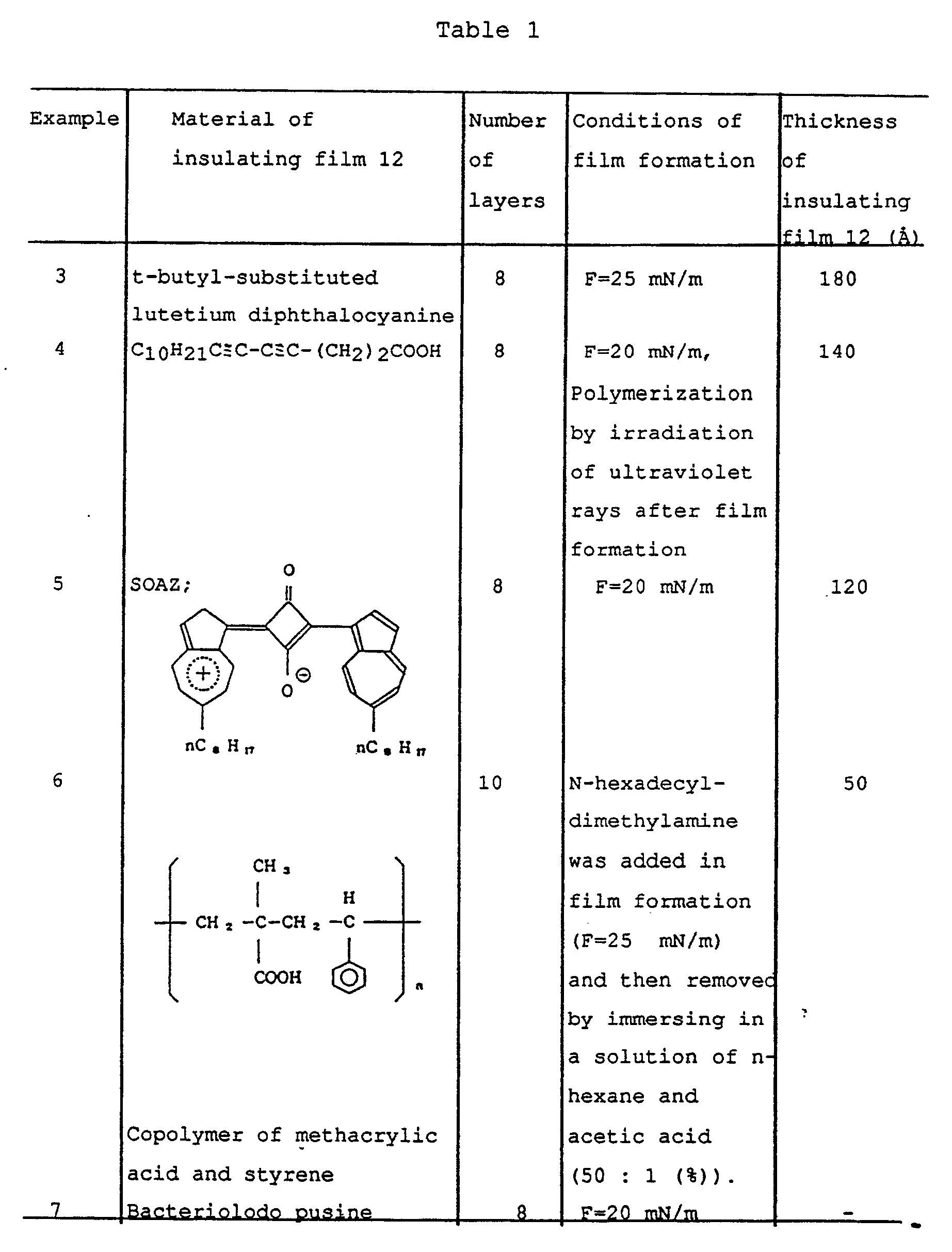
- Although each of the above-described examples utilizes the LB method as a method of forming the insulating thin films, the film formation method is not limited to the LB method and any other methods which are capable of forming insulating uniform microfilms can be used. Examples of film formation methods include vacuum deposition, electrolytic polymerization, CVD and the like, and wide-ranging materials can thus be used.
- With respect to the formation of electrodes, the method of forming electrodes is not limited to vacuum deposition and sputtering methods and any other methods which are capable of forming films on the insulating film can be used, such as described above.
- The material and shape of the substrate used in the present invention are not particularly limited.
-
- (1) The combination of a switching element having the MIM structure exhibiting an electrical switching phenomenon with a material or element having properties of photoelectric conversion enables the achievement of such optical switching characteristics as a result which has been not achieved so far.
- (2) The film formation of the molecular order can be easily realized by forming the "I region" in the MIM element using the LB method. This method exhibits excellent controlling properties and thus shows a high degree of reproducibility of the shape and properties of the switching element, as well as good productivity.
Claims (12)
- (1) A switching element comprising two electrodes and a region which is a selected one of insulative and semiconductive, interposed between said two electrodes, further comprising a photosensitive region having electrical characteristics which are changed by irradiation of light, said photosensitive region being arranged to control a electrical characteristic across said electrodes.
- (2) A switching element according to Claim 1, wherein the conductivity of said photosensitive region is changed by irradiation of light.
- (3) A switching element according to Claim 1, wherein an electromotive force is produced by irradiation of light in said photosensitive region.
- (4) A switching element according to Claim 1 having memory properties.
- (5) A switching element according to Claim 1, wherein said insulating/semiconductive region is composed of organic thin films and has a laminar structure.
- (6) A switching element according to Claim 5, wherein said laminar structure comprises layers formed by the LB method.
- (7) A switching element according to Claim 5, wherein thickness of each of said organic thin films is 5 to 500 Å.
- (8) A switching element comprising two electrodes and a region, which is selected one of insulative and conductive, interposed between said two electrodes, said region being formed of organic material.
- (9) A switching element according to Claim 8, wherein said region is composed of organic thin films and has a laminar structure.
- (10) A switching element according to Claim 9, wherein said laminar structure comprises layers formed by the LB method.
- (11) A switching element according to Claim 9, wherein the thickness of each of said organic thin films is 5 to 500 Å.
- (12) A switching element comprising an organic thin film and means for applying a voltage to the thin film, said film altering between a low resistance and a high resistance state dependency upon the field and maintaining its state until a voltage above a threshold value is applied.
Applications Claiming Priority (2)
| Application Number | Priority Date | Filing Date | Title |
|---|---|---|---|
| JP63039829A JP2675803B2 (en) | 1988-02-22 | 1988-02-22 | Switching element |
| JP39829/88 | 1988-02-22 |
Publications (3)
| Publication Number | Publication Date |
|---|---|
| EP0330395A2 true EP0330395A2 (en) | 1989-08-30 |
| EP0330395A3 EP0330395A3 (en) | 1990-05-30 |
| EP0330395B1 EP0330395B1 (en) | 1997-05-07 |
Family
ID=12563859
Family Applications (1)
| Application Number | Title | Priority Date | Filing Date |
|---|---|---|---|
| EP89301600A Expired - Lifetime EP0330395B1 (en) | 1988-02-22 | 1989-02-20 | Switching element |
Country Status (4)
| Country | Link |
|---|---|
| US (1) | US5170238A (en) |
| EP (1) | EP0330395B1 (en) |
| JP (1) | JP2675803B2 (en) |
| DE (1) | DE68928024T2 (en) |
Cited By (10)
| Publication number | Priority date | Publication date | Assignee | Title |
|---|---|---|---|---|
| EP0450921A2 (en) * | 1990-04-03 | 1991-10-09 | Canon Kabushiki Kaisha | Information transfer method, information transfer apparatus, and its driving method |
| WO1996038758A1 (en) * | 1995-05-30 | 1996-12-05 | Philips Electronics N.V. | Switching device and the use thereof |
| WO1998008139A1 (en) * | 1996-08-22 | 1998-02-26 | Philips Electronics N.V. | Electro-optical switching device |
| WO1998010329A1 (en) * | 1996-09-05 | 1998-03-12 | Philips Electronics N.V. | Optical switching device |
| WO1999039394A1 (en) * | 1998-02-02 | 1999-08-05 | Uniax Corporation | X-y addressable electric microswitch arrays and sensor matrices employing them |
| WO2003032405A1 (en) * | 2001-09-28 | 2003-04-17 | Japan Science And Technology Corporation | Photoelectric current multiplier using molecular crystal and production method therefor |
| WO2005041205A1 (en) * | 2003-10-22 | 2005-05-06 | Siemens Aktiengesellschaft | Rewritable memory unit made from organic materials |
| WO2005093870A1 (en) * | 2004-03-26 | 2005-10-06 | Thin Film Electronics Asa | An organic electronic device and methods for manufacturing a device of this kind |
| WO2006005016A1 (en) * | 2004-06-30 | 2006-01-12 | Hewlett-Packard Development Company L.P. | A molecular layer and method of forming the same |
| WO2006125730A1 (en) * | 2005-05-23 | 2006-11-30 | Siemens Aktiengesellschaft | Organic photodetector with a thin layer construction |
Families Citing this family (11)
| Publication number | Priority date | Publication date | Assignee | Title |
|---|---|---|---|---|
| EP0482920A3 (en) * | 1990-10-24 | 1993-01-07 | Kabushiki Kaisha Toshiba | Organic optical element |
| JP3437195B2 (en) * | 1991-10-01 | 2003-08-18 | キヤノン株式会社 | MIM type electric element, method of manufacturing the same, and image display device and drawing device using the same |
| CA2080251C (en) * | 1991-10-15 | 1997-12-02 | Shunichi Shido | Information processing apparatus with tracking mechanism |
| JPH06187675A (en) * | 1992-09-25 | 1994-07-08 | Canon Inc | Information processor and information processing method using the same |
| JP3207994B2 (en) * | 1993-02-17 | 2001-09-10 | キヤノン株式会社 | Scanning probe microscope and information recording / reproducing apparatus using the same |
| US6572974B1 (en) * | 1999-12-06 | 2003-06-03 | The Regents Of The University Of Michigan | Modification of infrared reflectivity using silicon dioxide thin films derived from silsesquioxane resins |
| WO2006022017A1 (en) | 2004-08-27 | 2006-03-02 | Fuji Electric Holdings Co., Ltd. | Logic circuit |
| EP2377166A4 (en) * | 2008-12-18 | 2015-06-24 | First Solar Inc | Photovoltaic devices including back metal contacts |
| JP5560727B2 (en) * | 2009-08-28 | 2014-07-30 | ソニー株式会社 | Non-wetted all solid protein photoelectric conversion device, method for producing the same, and electronic device |
| DE102019123088A1 (en) * | 2019-08-28 | 2021-03-04 | TPMT-Tepin Microelectronic Technology Ltd. Co. | Photoswitch structure, associated manufacturing process and arrangement with a photoswitch structure and a voltage source |
| DE102019123085A1 (en) * | 2019-08-28 | 2021-03-04 | TPMT-Tepin Microelectronic Technology Ltd. Co. | Solar cell, associated manufacturing and operating process and arrangement with a solar cell and a voltage source |
Citations (3)
| Publication number | Priority date | Publication date | Assignee | Title |
|---|---|---|---|---|
| EP0244835A2 (en) * | 1986-05-09 | 1987-11-11 | Nippon Oil And Fats Company, Limited | Langmuir-Blodgett ultrathin membrane of polyfumurate |
| EP0268370A2 (en) * | 1986-10-13 | 1988-05-25 | Canon Kabushiki Kaisha | Switching device |
| EP0272937A2 (en) * | 1986-12-24 | 1988-06-29 | Canon Kabushiki Kaisha | Switching device |
Family Cites Families (6)
| Publication number | Priority date | Publication date | Assignee | Title |
|---|---|---|---|---|
| US3833894A (en) * | 1973-06-20 | 1974-09-03 | Ibm | Organic memory device |
| JPS58221562A (en) * | 1982-06-18 | 1983-12-23 | Fuji Xerox Co Ltd | Original reader |
| US4731756A (en) * | 1983-02-07 | 1988-03-15 | The Johns Hopkins University | Optical storage and switching devices using organic charge transfer salts |
| JPS60193326A (en) * | 1984-03-15 | 1985-10-01 | Canon Inc | Film forming apparatus |
| JPS60194517A (en) * | 1984-03-16 | 1985-10-03 | Canon Inc | Forming method of monomolecular laminated film |
| GB2202085B (en) * | 1987-01-27 | 1990-02-14 | Ricoh Kk | Amorphous silicon photosensor |
-
1988
- 1988-02-22 JP JP63039829A patent/JP2675803B2/en not_active Expired - Lifetime
-
1989
- 1989-02-20 DE DE68928024T patent/DE68928024T2/en not_active Expired - Fee Related
- 1989-02-20 EP EP89301600A patent/EP0330395B1/en not_active Expired - Lifetime
- 1989-02-22 US US07/313,499 patent/US5170238A/en not_active Expired - Lifetime
Patent Citations (3)
| Publication number | Priority date | Publication date | Assignee | Title |
|---|---|---|---|---|
| EP0244835A2 (en) * | 1986-05-09 | 1987-11-11 | Nippon Oil And Fats Company, Limited | Langmuir-Blodgett ultrathin membrane of polyfumurate |
| EP0268370A2 (en) * | 1986-10-13 | 1988-05-25 | Canon Kabushiki Kaisha | Switching device |
| EP0272937A2 (en) * | 1986-12-24 | 1988-06-29 | Canon Kabushiki Kaisha | Switching device |
Non-Patent Citations (3)
| Title |
|---|
| APPLIED PHYSICS LETTERS, vol. 41, no. 6, September 1982, pages 548-550, American Institute of Physics, New York, US; R.S. POTEMBER et al.: "Optical switching in semiconductor organic thin films" * |
| ELECTRONICS INTERNATIONAL, vol. 55, no. 15, July 1982, pages 47-48, New York, US; R. CONNOLLY: "Light, electric pulses switch organic films" * |
| THIN SOLID FILMS, vol. 149, no. 2, 25th May 1987, pages 163-170, Elsevier Sequota, Lausanne, CH; Y.L. HUA et al.: "Photoelectric properties of substituted silicon phthalocyanine langmuir-blodgett film schottky barrier and metal/insulator/semiconductor devices" * |
Cited By (20)
| Publication number | Priority date | Publication date | Assignee | Title |
|---|---|---|---|---|
| EP0450921A2 (en) * | 1990-04-03 | 1991-10-09 | Canon Kabushiki Kaisha | Information transfer method, information transfer apparatus, and its driving method |
| EP0450921A3 (en) * | 1990-04-03 | 1992-05-13 | Canon Kabushiki Kaisha | Information transfer method, information transfer apparatus, and its driving method |
| US5274475A (en) * | 1990-04-03 | 1993-12-28 | Canon Kabushiki Kaisha | Information transfer method, information transfer apparatus, and its driving method |
| WO1996038758A1 (en) * | 1995-05-30 | 1996-12-05 | Philips Electronics N.V. | Switching device and the use thereof |
| WO1998008139A1 (en) * | 1996-08-22 | 1998-02-26 | Philips Electronics N.V. | Electro-optical switching device |
| WO1998010329A1 (en) * | 1996-09-05 | 1998-03-12 | Philips Electronics N.V. | Optical switching device |
| US6864111B2 (en) | 1998-02-02 | 2005-03-08 | E. I. Du Pont De Nemours And Company | Column-row addressable electric microswitch arrays and sensor matrices employing them |
| US6707060B2 (en) | 1998-02-02 | 2004-03-16 | E. I. Du Pont De Nemours And Company | Column-row addressable electric microswitch arrays and sensor matrices employing them |
| WO1999039394A1 (en) * | 1998-02-02 | 1999-08-05 | Uniax Corporation | X-y addressable electric microswitch arrays and sensor matrices employing them |
| US6441395B1 (en) | 1998-02-02 | 2002-08-27 | Uniax Corporation | Column-row addressable electric microswitch arrays and sensor matrices employing them |
| WO2003032405A1 (en) * | 2001-09-28 | 2003-04-17 | Japan Science And Technology Corporation | Photoelectric current multiplier using molecular crystal and production method therefor |
| US7294780B2 (en) | 2001-09-28 | 2007-11-13 | Japan Science And Technology Agency | Photoelectric current multiplier using molecular crystal and production method therefor |
| US7220986B2 (en) | 2001-09-28 | 2007-05-22 | Japan Science & Technology Agency | Photoelectric current multiplier using molecular crystal and production method therefor |
| WO2005041205A1 (en) * | 2003-10-22 | 2005-05-06 | Siemens Aktiengesellschaft | Rewritable memory unit made from organic materials |
| US7265379B2 (en) | 2004-03-26 | 2007-09-04 | Thin Film Electronics Asa | Organic electronic device and methods for manufacturing a device of this kind |
| WO2005093870A1 (en) * | 2004-03-26 | 2005-10-06 | Thin Film Electronics Asa | An organic electronic device and methods for manufacturing a device of this kind |
| WO2006005016A1 (en) * | 2004-06-30 | 2006-01-12 | Hewlett-Packard Development Company L.P. | A molecular layer and method of forming the same |
| US7255892B2 (en) | 2004-06-30 | 2007-08-14 | Hewlett-Packard Development Company, L.P. | Molecular layer and method of forming the same |
| US7875348B2 (en) | 2004-06-30 | 2011-01-25 | Hewlett-Packard Development Company, L.P. | Molecular layer and method of forming the same |
| WO2006125730A1 (en) * | 2005-05-23 | 2006-11-30 | Siemens Aktiengesellschaft | Organic photodetector with a thin layer construction |
Also Published As
| Publication number | Publication date |
|---|---|
| DE68928024T2 (en) | 1997-10-02 |
| DE68928024D1 (en) | 1997-06-12 |
| EP0330395B1 (en) | 1997-05-07 |
| JPH01214078A (en) | 1989-08-28 |
| EP0330395A3 (en) | 1990-05-30 |
| JP2675803B2 (en) | 1997-11-12 |
| US5170238A (en) | 1992-12-08 |
Similar Documents
| Publication | Publication Date | Title |
|---|---|---|
| EP0330395B1 (en) | Switching element | |
| EP0272937B1 (en) | Switching device | |
| US5359204A (en) | Switching device | |
| US5020881A (en) | Light modulating device with optical switching unit of laminated insulating and conductive layers | |
| US4939556A (en) | Conductor device | |
| Roberts et al. | Electronic devices incorporating stable phthalocyanine Langmuir-Blodgett films | |
| US5136212A (en) | Electron emitting device, electron generator employing said electron emitting device, and method for driving said generator | |
| EP0294061B1 (en) | Optical modulators based on polymers | |
| US20030010973A1 (en) | Polymer semiconductor device comprising at least a rectifying function and mehtod for making same | |
| US5798197A (en) | Use of low molecular-weight or polymeric organic compounds which are present in the columnar-helical phase and have liquid-crystalline properties | |
| Hua et al. | Photoelectric properties of substituted silicon phthalocyanine Langmuir-Blodgett film Schottky barrier and metal/insulator/semiconductor devices | |
| EP0114851A1 (en) | Polymeric films | |
| JPS6396956A (en) | Switching element | |
| Tanikawa et al. | Rectification effects based on the p‐n junction of poly [γ‐(β‐N‐carbazolylethyl)‐L‐glutamate]—2, 4, 7‐trinitrofluorenone systems | |
| EP0329432B1 (en) | Electron emitter | |
| Nabok et al. | Electrical study of polyelectrolyte self-assembled films using mercury probe | |
| JP2715301B2 (en) | Photoelectron beam conversion element | |
| JPH01147873A (en) | Switching element | |
| Sharma et al. | Study of some organic polymeric materials for electrical and optoelectrical devices | |
| JPH0779173B2 (en) | Semiconductor element | |
| JPS6316071A (en) | Organic membrane | |
| Kim et al. | I–V and π− A characteristics of ultrathin Langmuir-Blodgett films | |
| JPH04306262A (en) | Polymer composite material containing dispersed organic fine particle and its production | |
| Rath et al. | Organic Memory and Electrical Bistability in a Quinone-Based Charge-Transfer Complex | |
| JPS63160389A (en) | Switching device |
Legal Events
| Date | Code | Title | Description |
|---|---|---|---|
| PUAI | Public reference made under article 153(3) epc to a published international application that has entered the european phase |
Free format text: ORIGINAL CODE: 0009012 |
|
| AK | Designated contracting states |
Kind code of ref document: A2 Designated state(s): DE FR GB NL |
|
| PUAL | Search report despatched |
Free format text: ORIGINAL CODE: 0009013 |
|
| AK | Designated contracting states |
Kind code of ref document: A3 Designated state(s): DE FR GB NL |
|
| 17P | Request for examination filed |
Effective date: 19901017 |
|
| 17Q | First examination report despatched |
Effective date: 19921218 |
|
| GRAG | Despatch of communication of intention to grant |
Free format text: ORIGINAL CODE: EPIDOS AGRA |
|
| GRAH | Despatch of communication of intention to grant a patent |
Free format text: ORIGINAL CODE: EPIDOS IGRA |
|
| GRAH | Despatch of communication of intention to grant a patent |
Free format text: ORIGINAL CODE: EPIDOS IGRA |
|
| GRAA | (expected) grant |
Free format text: ORIGINAL CODE: 0009210 |
|
| RAP1 | Party data changed (applicant data changed or rights of an application transferred) |
Owner name: CANON KABUSHIKI KAISHA |
|
| AK | Designated contracting states |
Kind code of ref document: B1 Designated state(s): DE FR GB NL |
|
| REF | Corresponds to: |
Ref document number: 68928024 Country of ref document: DE Date of ref document: 19970612 |
|
| ET | Fr: translation filed | ||
| PLBE | No opposition filed within time limit |
Free format text: ORIGINAL CODE: 0009261 |
|
| STAA | Information on the status of an ep patent application or granted ep patent |
Free format text: STATUS: NO OPPOSITION FILED WITHIN TIME LIMIT |
|
| 26N | No opposition filed | ||
| REG | Reference to a national code |
Ref country code: GB Ref legal event code: IF02 |
|
| PGFP | Annual fee paid to national office [announced via postgrant information from national office to epo] |
Ref country code: GB Payment date: 20040206 Year of fee payment: 16 |
|
| PGFP | Annual fee paid to national office [announced via postgrant information from national office to epo] |
Ref country code: NL Payment date: 20040216 Year of fee payment: 16 |
|
| PGFP | Annual fee paid to national office [announced via postgrant information from national office to epo] |
Ref country code: FR Payment date: 20040223 Year of fee payment: 16 |
|
| PGFP | Annual fee paid to national office [announced via postgrant information from national office to epo] |
Ref country code: DE Payment date: 20040225 Year of fee payment: 16 |
|
| PG25 | Lapsed in a contracting state [announced via postgrant information from national office to epo] |
Ref country code: GB Free format text: LAPSE BECAUSE OF NON-PAYMENT OF DUE FEES Effective date: 20050220 |
|
| PG25 | Lapsed in a contracting state [announced via postgrant information from national office to epo] |
Ref country code: NL Free format text: LAPSE BECAUSE OF NON-PAYMENT OF DUE FEES Effective date: 20050901 Ref country code: DE Free format text: LAPSE BECAUSE OF NON-PAYMENT OF DUE FEES Effective date: 20050901 |
|
| GBPC | Gb: european patent ceased through non-payment of renewal fee |
Effective date: 20050220 |
|
| PG25 | Lapsed in a contracting state [announced via postgrant information from national office to epo] |
Ref country code: FR Free format text: LAPSE BECAUSE OF NON-PAYMENT OF DUE FEES Effective date: 20051031 |
|
| NLV4 | Nl: lapsed or anulled due to non-payment of the annual fee |
Effective date: 20050901 |
|
| REG | Reference to a national code |
Ref country code: FR Ref legal event code: ST Effective date: 20051031 |