EP0327782A1 - Steuerungsblockverarbeitungssystem für Bussteuerung - Google Patents
Steuerungsblockverarbeitungssystem für Bussteuerung Download PDFInfo
- Publication number
- EP0327782A1 EP0327782A1 EP88630022A EP88630022A EP0327782A1 EP 0327782 A1 EP0327782 A1 EP 0327782A1 EP 88630022 A EP88630022 A EP 88630022A EP 88630022 A EP88630022 A EP 88630022A EP 0327782 A1 EP0327782 A1 EP 0327782A1
- Authority
- EP
- European Patent Office
- Prior art keywords
- bus
- command
- integrated circuit
- bit
- cpu
- Prior art date
- Legal status (The legal status is an assumption and is not a legal conclusion. Google has not performed a legal analysis and makes no representation as to the accuracy of the status listed.)
- Withdrawn
Links
Images


Classifications
-
- G—PHYSICS
- G06—COMPUTING; CALCULATING OR COUNTING
- G06F—ELECTRIC DIGITAL DATA PROCESSING
- G06F13/00—Interconnection of, or transfer of information or other signals between, memories, input/output devices or central processing units
- G06F13/14—Handling requests for interconnection or transfer
- G06F13/20—Handling requests for interconnection or transfer for access to input/output bus
- G06F13/28—Handling requests for interconnection or transfer for access to input/output bus using burst mode transfer, e.g. direct memory access DMA, cycle steal
Definitions
- the field of the invention is that of control of system buses in digital systems, in particular in systems that employ the MIL-STD-1553 bus.
- the 1553 bus has been defined by the Department of Defense as an asynchronous, serial, time division multiplex bus.
- a typical 1553 system there will be one central computer (such as a fire control computer on an airplane) and a number of other units on the bus which are referred to as remote terminals (RT).
- the detailed bus requirements are defined in a number of available publications, including the MIL-STD 1553 Multiplex Applications Handbook from SCI Systems, Inc., of Huntsville, Alabama.
- the standard also allows for three word formats - command words, data words, and status words, having the obvious functions.
- the bus standard also provides for three catagories of message formats - message transfers between any two remote terminals (RT to RT), transfers from the bus controller to a particular terminal; mode commands for terminal management; and broadcasts to all remote terminals.
- a further load on the central computer is the necessity for the CPU to reconfigure the message sequence that is being sent over the bus in order to respond to events that have sent an interrupt signal to the CPU.
- Another drawback of some previous systems is that there have been fixed requirements on the memory areas used and the size of those areas. Both of the above problems require more intervention by the CPU.
- the invention relates to an implementation of a 1553 bus controller that includes the low voltage logic and control functions required by the military standard on a single chip and offloads from the CPU many tasks of managing the bus.
- a feature of the invention is that all commands and data relating to 1553 bus messages are stored within the host memory related to the CPU and accessed by the bus controller chip by using DMA techniques.
- Another feature of the invention is the provision of a linked list of messages which the bus controller will execute independently of the CPU in a programmed sequence determined by the systems programmer, deviating from the sequence as required only in accordance with commands from the CPU.
- the linked list of messages corresponds to a linked list of command block areas of memory.
- Another feature of the invention is the provision of a dual-purpose chip that may perform the bus interface operations for either a bus controller or a remote terminal and is referred to herein as a BCRT (Bus Controller - Remote Terminal).
- BCRT Bus Controller - Remote Terminal
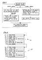
- FIG. 1 there is shown schematically a portion of a bus control system constructed according to the invention.
- a two wire bus indicated by the numeral 5 is the dual twisted-pair bus required by the 1553 specification.
- Two transformers 32 and 34 couple signals to the bus.
- a bus interface unit 30 translates signals from logic levels used on the chip to the mil spec levels required. All of the foregoing are conventional units that are not part of this invention.
- microprocessor 10 On the right of the drawing is a 16 bit microprocessor 10, illustratively a Motorola 68000 microprocessor. This is the central processing unit of the bus of a digital system that employs the 1553 bus. Other systems on the 1553 bus will be referred to as remote terminals (RT), even though they may contain other local CPU's.
- memory module 20 On the top of the drawing is a memory module 20 which is the host memory associated with the CPU.
- a conventional memory control logic device 25 receives control signals from both the CPU and from the bus controller chip.
- CPU 10, memory 20 and memory control 25 are all commercially available units. The invention may be practical with any of a number of embodiments of these units.
- the bus controller chip of the invention denoted by the numeral 100, has an address bus 12 and a data bus 14 going to both the memory and to the CPU and control lines also going to both the memory and the CPU.
- the control signals provided are flexible in order to interface with many units.
- the CPU may write directly into registers within bus controller 100 in order to initialize the set of tasks to be performed and to modify the set of tasks in accordance with whatever system program the CPU is running.
- Bus controller 100 sends data to the CPU and also sends data directly into memory 20 using a conventional DMA (direct memory access) procedure.
- bus controller 100 will send commands along bus 5 to various remote units that are part of the system; receive responses from those remote units and ordinarily store responses in memory 20.
- controller 100 may transmit data or flags that are referred to as interrupts back to the CPU.
- An advantage of the direct storing of data in memory unit 20 is that it may be accessed by the CPU 10 as is convenient for the overall system operation. Prior art controllers forced the CPU to interrupt its work in order to handle data.
- Bus controller 100 must, of course, carry out all of the functions required by the 1553 standard, including sending commands to individual units, sending broadcast commands, and controlling transfers of messages from one remote unit to another.
- the advantage of this invention is not only that it accomplishes the functions in a single chip, but that it also reduces the load on the CPU.
- bus controller 100 there is shown a block diagram of bus controller 100.
- encoder/decoder 102 converts parallel data to serial form and applies the conventional Manchester II coding scheme as required by the standard.
- Unit 102 is controlled in turn by bus control module 104, a simple finite state machine the sequence of which is shown in Figure 3.
- the normal waiting state is at the top of the figure waiting for a request from the command block processor 110 to perform a bus transfer. If the transfer is a receive, unit 104 waits for a word to be received on decoder 102 and then transfers the word along an internal bus to either an internal register within unit 126 or unit 124 or to DMA sequencer 120 to be passed to host memory 20.
- unit 104 passes a control signal back to the module that initiated the request and then resumes the wait state. Construction of finite state machines is well known to those skilled in the art and many different embodiments will do equally well. A source of information on the design of finite state machines is (references).
- DMA sequencer 120 performs a conventional DMA sequence, well known to those skilled in the art, in which, upon receipt of a control signal it initiates arbitration of the local bus shared by the CPU and memory 20, transmits an address and internal data path control signals to memory unit 20 and/or memory control logic 25.
- DMA sequencer 120 sends a completion signal back to the requesting module and resumes the waiting state.
- Data is received directly from the memory or written directly from the CPU on bus 14 which connects with a set of user registers 124 which may be accessed by the CPU and a set of internal registers 126 that are not user- accessible. Data moves between these registers and other modules within unit 100 under control of the main finite state machine, referred to as the command block processor 110.
- a finite state machine may be implemented in a number of embodiments, such as a programmed logic array (PLA), or a ROM, which is a specialized PLA.
- PLA programmed logic array
- ROM read-only memory
- the operation of the microcode in a microprocessor is an example of a finite state machine that is analogous to bus controller command block processor 110.
- Subsidiary modules that provide optional features are interrupt handler 130 which responds to data received from the bus to set flags within an appropriate register and to initiate control signals to the CPU. These signals may enter the CPU through one of its interrupt channels or may reside within a register waiting for the CPU to interrogate a register, as is required by the system program that the CPU is executing.
- Timer 112 is a conventional clock that permits an improved feature of the subject invention compared to the prior art, in that block processor 110 can be programmed by the CPU to pause for a predetermined amount of time, which amount of time may be varied under stored program control, to exercise a series of message transfers and operations on the bus as required by the system program. For example, the system program may send a command through the bus controller to another unit on the bus. After the remote unit has had time to carry out the command, the bus controller may then execute a data transfer to store the resultant data in host memory, all without intervention by the CPU.
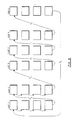
- Block 410 is the nth block in a chain of command blocks that is set up by the systems programmer and block 420 is the (n + 1)th block.
- the bus controller will execute the command defined by the nth command block and then load the contents of word 418 which is a memory address pointing to the next (n + 1) command block to be executed.
- the link is shown symbolically by an arrow connecting word 418 to word 421 in the drawing.
- the bus controller executes a DMA to fetch the contents of words 412, 413, and 415.
- the head pointer, word 411 has previously been stored in a register within the bus controller, either by the host CPU or by the process of reading the tail pointer (416 or 428) of a previous command block:
- the command word is a 1553 bus command which is set in a format dictated by the mil spec requirements.
- the control word contains information directing the bus controller in the manner in which it will manage the process of sending the command word out on the system bus and responding to whatever signal is returned.
- word 414 is a second position for a second command word that is used only in the particular case in which there is a transfer between two remote terminals.
- Word 415 is a data pointer pointing to an area of host memory that contains data that is relevant to this command or where data will be stored.
- the two status words 416 and 417 have a format dictated also by the mil spec.
- the tail pointer as previously described, contains the address in host memory of the next command block.
- the control word is a 16 bit word written by the host CPU with bit selectable options for the bus controller. Bits 0 through 7 set a time delay between the beginning of this command block and the beginning of the execution of the next command block in sequence. Bit 8 provides an option to monitor the transfer of a message between two remote terminals. Bit 8 indicates that the message should be received and stored beginning at the location indicated by the data pointer in the command block being executed. Bit 9 is a flag indicating that the command block is a remote terminal to remote terminal transfer. Bit 10 is a flag indicating that the bus controller should halt and send an interrupt to the CPU after the execution of this command. Bit 11 enables the retry function to retry a command.
- Bit 12 enables a polling operation of the remote units by the bus controller without intervention from the CPU.
- Polling refers to bus controller interrogation of remote terminals by requesting transmission of their status words.
- the BCRT enables the host to initialize a chain of command blocks with the polling enable bit set.
- a polling compare register containing a word stored by the host also exists. The remote terminal response in the polling mode is compared to the contents of the Polling Compare Register. If the comparison results in any matching bits, a standard interrupt (if so enabled) is asserted.
- Bit 13 provides for an option in which the bus controller asserts an interrupt to the CPU and continues processing the list of messages.
- Bit 15 is a flag set by the bus controller indicating that there was an error in the execution of this command. Bit 14 indicates that this command block should be skipped and the next command block in sequence should be executed.
- this system provides a rich variety of options for the systems programmer to offload a great burden from the CPU by initializing a message list of commands to be executed and alternative list sequences that the bus controller will be switched to on the occurrence of any of several anticipated conditions.
- the basic list may be a standard pattern of interrogating the remote terminals with as many optional sequences as required.
- the subject invention By implementing a linked list message scheme, the subject invention enables the host CPU to easily implement transaction loops and message list moves as well as message scheduling routines. The invention accomplishes this by using internal state machines, timers and a linked pointer scheme implicit within the linked list message scheme.
- Competitors' products namely the DDC 66300/66305-65600 by ILC Data Device Corp. are inferior because they do not easily provide for message transaction loops, message list moves or message scheduling.
- the DDC product merely provides a method for message sequencing. In other words, with the DDC product, a host can simply set the messages to be transacted, in their respective order. There is no easy way to implement message schedules; it would be difficult to do message list jumps and impossible to do automatic message loops.
- the BCRT can be set up to do so easily as shown in Figure 6, which shows the area of memory containing the linked list of command blocks, with arrows indicating that the head and tail pointers carry the connecting information.
- Ts delay times that are set by the systems programmer to produce the desired timing.
- the subject invention offloads from the host CPU many of the tasks associated with this common application.
- the remote terminal units may be configured to send a message to the bus controller that will cause an interrupt to the CPU which will branch to a message handling routine that will respond to whatever event caused the flag to be sent.
- the above example may be modified by providing that an event, such as the identification of a hostile aircraft will cause the message sequence to add another list D to the sequence.
- the CPU will presumably be involved to make a decision to switch operating modes of the system. It may do so by merely resetting one tail pointer to pass control from the second occurrence of list C, say, to list D.
- List D will already have had its last tail pointer set to the second occurrence of list B, so that only the one change referred to above will alter the system operating mode.
- Those skilled in the art will readily be able to devise more complex variations ⁇ of lists to satisfy their system needs with less interaction by the CPU than would be required if prior art devices were used.
- FIG. 5 there is shown a state diagram of the block processor 110 which is a finite state machine that controls the operation of the bus controller in response to the different states.
- the default wait state is indicated by the block labeled idle, in which the bus controller is waiting for a command.
- the numeral 8 indicates a branch from a previous command block.
- the first operation block which is a DMA execution, may be reached by a signal from the CPU to switch the bus controller from the idle state to execute a message or by a signal from the previous command block to continue executing the next block in sequence.
- the bus controller executes a DMA to fetch the control word, the first command word and the data pointer.
- the second command word is not fetched at this time because it is not known if that command word will be used and it is desired to make response as fast as possible.
- the bus controller next checks only that the control word and the command word are acceptable and, if so, immediately sends the first command word out on the system bus in order to accomplish the message transfer in the shortest possible time.
- the symbol X indicates a branch to an interrupt/error sequence shown in Figure 5g.
- the controller checks the control word and first command word and branches to one of four branches, as shown in Figure 5b depending upon whether the command is an RT to RT command, a transmit command, a receive command, or a mode code command.
- the second command word is then fetched and the series of steps shown in Figure 5c are executed. This path then branches to the normal receive steps in Figure 5e as described below.
- the steps as shown in Figure 5d are executed with a branch for two forms of transfer -single word and multi word and a further branch for a broadcast command.
- the series of steps for a receive command is indicated. Since the command has been previously been put on the bus, the first step in this drawing is to load a response from the remote terminal from the bus into the bus controller.
- the status word is defined by the mil spec and will be processed by the CPU.
- the status word is loaded into the host memory in order that the CPU may access it when the system program calls for that, not in response to an interrupt from the bus controller.
- the last form of command shown in Figure 5f is a broadcast command in which the command is sent to all the remote terminals.
- Figure 5g shows a series of steps to accomodate an error and to return control back to the start.
- Table 1 shows a list of the pins on the bus controller unit in two forms, that of a leadless chip carrier and a PGA.
- the signals, their type and the description are listed in a self-explanatory fashion.
- Table 2 shows a list of the internal registers of the bus controller.
- Table 3 shows a list of internal registers that are not accessible to the user.
- Unit 210 shown in dotted outline, is an optional finite state machine that controls the operation of the dual-purpose chip to perform similar bus interface functions for a remote terminal.
- Signal BCRTSEL determines the Bus Controller or Remote Terminal mode of operation. It can be overridden by using the BC/RT Mode Select bit in the Control register.
- One advantage of this feature is that the systems program may be written to permit more than one unit to function as the bus controller at different times.
- the architecture of the remote terminal system is that a local CPU and local memory are connected to the BCRT chip as shown in Figure 1.
- a descriptor space that contains a number of four-word blocks, of which three words are used. Two blocks referred to as descriptors are used for each sub-address, which is a field in the RT Command Word - one for transmit and one for receive.
- the descriptors are stored in local RAM in a list ordered sequentially by sub-address and initialized by the CPU to control the execution of a data transfer associated with that sub-address.
- Each descriptor consists of four words, three of which are programmed by the CPU. These words indicate how to perform the data transfer associated with a designated sub-address.
- Control Word - The first word in the descriptor is the control word.
- the control word is used to select or disable message transfers and to select an index.
- Indexing refers to having a prespecified number (i.e., index) of messages transacted before the host CPU is notified. After each message transaction, the BCRT decre ments the index by one. It can be used by the host to determine the number of messages executed or be notified when the specified quantity has transacted.
- BIT 7 Interrupt when index 0. This bit is used by the host to indicate to the BCRT that an interrupt should be asserted when the index is decremented to zero.
- the Data List Pointer is the second word within the descriptor. This word is set by the host and used by the BCRT to store data in RAM beginning at the data list pointer address.
- Message Status Pointer This word, the third within the descriptor, is set by the host and used by the BCRT to store message status information in RAM beginning at the message status pointer.
- Each message transacted by the BCRT has a corresponding message status word. This word allows the host CPU to evaluate the message's validity, determine the word count, and calculate the approximate time frame in which the message is transacted.
- BITs 0-7 Time tag These are written by the BCRT after message completion. The resolution is sixty- four microseconds.
- BITs 8-12 Word count This indicates the number of words in the message and reflects the word count field in the command word. Should the message contain a different number of words than the word count field, the message error flag will be triggered. If there are excessive words they will be withheld from RAM. If the actual word count is less than it should be, the ME bit is set and the data pointer is incremented by the amount specified in the word count field.
- Registers have been implemented to enable the CPU to control the actions of the BCRT while still maintaining low DMA overhead by the BCRT. All functions are active high and ignored when low unless otherwise mentioned. Functions/parameters are used in both RT and BC modes except where indicated. Registers are addressed by the binary equivalent of their decimal number - i.e. Register #1 is addressed as 0001B. All registers have read/write capability. Register usage is defined as follows:
- the bits indicate the BCRT's current status.
- RT Remote Terminal Descriptor Space Address Register. This is initialized by the host to indicate the starting location of the RT descriptor space. The host must allow 320 sequential locations following this starting address. NOTE: This location, for proper operation must start on a X512D address boundary. (Where "X" is an integer multiple.)
- the Polling Compare Register is set by the CPU to indicate the RT response word on which the BCRT should interrupt.
- This register is eleven bits wide, corresponding to bits 9 - 19 of the RT's Status Word response. (i.e. The sync, Remote Terminal Address and parity bits are not included.) (See section on Polling.) #4 BIT (Built-In-Test) Word Register
- this register contains the current command being executed. If the BCRT is not active, this register will contain the last command executed. #6 Interrupt Log List Pointer Register
- the Interrupt Log List Pointer Register indicates the start of the Interrupt Log List. After each list entry, the BCRT updates this register with the address of where the next entry will be in the list.
- this register When a high priority interrupt is asserted, this register will indicate the event that caused it.' To clear the interrupt signal and reset the bit, a high signal should be written to the appropriate bit. See the corresponding bit definition of register #7.
- This register is used to enable the standard interrupt caused by any one of the following enabled events.
- This register is used to set the Remote Terminal Address via software.
- the Change Lock-Out Enable feature when set, prevents the Remote Terminal Address or the BC/RT mode selection from changing.
Priority Applications (2)
| Application Number | Priority Date | Filing Date | Title |
|---|---|---|---|
| EP88630022A EP0327782A1 (de) | 1988-02-08 | 1988-02-08 | Steuerungsblockverarbeitungssystem für Bussteuerung |
| DE1988630022 DE327782T1 (de) | 1988-02-08 | 1988-02-08 | Steuerungsblockverarbeitungssystem fuer bussteuerung. |
Applications Claiming Priority (1)
| Application Number | Priority Date | Filing Date | Title |
|---|---|---|---|
| EP88630022A EP0327782A1 (de) | 1988-02-08 | 1988-02-08 | Steuerungsblockverarbeitungssystem für Bussteuerung |
Publications (1)
| Publication Number | Publication Date |
|---|---|
| EP0327782A1 true EP0327782A1 (de) | 1989-08-16 |
Family
ID=8200527
Family Applications (1)
| Application Number | Title | Priority Date | Filing Date |
|---|---|---|---|
| EP88630022A Withdrawn EP0327782A1 (de) | 1988-02-08 | 1988-02-08 | Steuerungsblockverarbeitungssystem für Bussteuerung |
Country Status (2)
| Country | Link |
|---|---|
| EP (1) | EP0327782A1 (de) |
| DE (1) | DE327782T1 (de) |
Cited By (5)
| Publication number | Priority date | Publication date | Assignee | Title |
|---|---|---|---|---|
| EP0422776A2 (de) * | 1989-10-11 | 1991-04-17 | International Business Machines Corporation | Seriellübertragungsvorrichtung zum Empfangen von Seriellübertragungszustandsdaten mit einer DMA-Steuereinheit |
| EP0428111A2 (de) * | 1989-11-14 | 1991-05-22 | Hitachi, Ltd. | Datenübertragungssteuerungsverfahren und Datenprozessor, der dieses verwendet |
| AU644814B2 (en) * | 1990-02-02 | 1993-12-23 | Auspex Systems, Inc. | Direct memory access controller |
| WO2010015434A1 (en) * | 2008-08-07 | 2010-02-11 | Icera Inc | Dma engine |
| CN114328311A (zh) * | 2021-12-15 | 2022-04-12 | 珠海一微半导体股份有限公司 | 一种存储控制器架构、数据处理电路及数据处理方法 |
Citations (1)
| Publication number | Priority date | Publication date | Assignee | Title |
|---|---|---|---|---|
| GB2142175A (en) * | 1983-06-16 | 1985-01-09 | Hitachi Ltd | Data transmission system |
-
1988
- 1988-02-08 EP EP88630022A patent/EP0327782A1/de not_active Withdrawn
- 1988-02-08 DE DE1988630022 patent/DE327782T1/de active Pending
Patent Citations (1)
| Publication number | Priority date | Publication date | Assignee | Title |
|---|---|---|---|---|
| GB2142175A (en) * | 1983-06-16 | 1985-01-09 | Hitachi Ltd | Data transmission system |
Non-Patent Citations (1)
| Title |
|---|
| ELECTRONIC DESIGN, vol. 35, no. 18, 6th August 1987, pages 109-114, Hasbrouck Heights, NJ, US; D.R. SNYDER: "Control MIL-STD-1553 with remote terminal chips" * |
Cited By (10)
| Publication number | Priority date | Publication date | Assignee | Title |
|---|---|---|---|---|
| EP0422776A2 (de) * | 1989-10-11 | 1991-04-17 | International Business Machines Corporation | Seriellübertragungsvorrichtung zum Empfangen von Seriellübertragungszustandsdaten mit einer DMA-Steuereinheit |
| EP0422776A3 (en) * | 1989-10-11 | 1993-09-22 | International Business Machines Corporation | Serial communication apparatus for receiving serial communication status data with a dma controller |
| EP0428111A2 (de) * | 1989-11-14 | 1991-05-22 | Hitachi, Ltd. | Datenübertragungssteuerungsverfahren und Datenprozessor, der dieses verwendet |
| EP0428111A3 (en) * | 1989-11-14 | 1992-12-30 | Hitachi, Ltd. | Data transfer control method and data processor using the same |
| AU644814B2 (en) * | 1990-02-02 | 1993-12-23 | Auspex Systems, Inc. | Direct memory access controller |
| WO2010015434A1 (en) * | 2008-08-07 | 2010-02-11 | Icera Inc | Dma engine |
| GB2474983A (en) * | 2008-08-07 | 2011-05-04 | Icera Inc | DMA engine |
| GB2474983B (en) * | 2008-08-07 | 2012-11-07 | Nvidia Technology Uk Ltd | DMA engine |
| US8589602B2 (en) | 2008-08-07 | 2013-11-19 | Icera, Inc. | Data transfer engine with delay circuitry for blocking transfers |
| CN114328311A (zh) * | 2021-12-15 | 2022-04-12 | 珠海一微半导体股份有限公司 | 一种存储控制器架构、数据处理电路及数据处理方法 |
Also Published As
| Publication number | Publication date |
|---|---|
| DE327782T1 (de) | 1989-12-07 |
Similar Documents
| Publication | Publication Date | Title |
|---|---|---|
| US4805137A (en) | Bus controller command block processing system | |
| US4133030A (en) | Control system providing for the transfer of data in a communications processing system employing channel dedicated control blocks | |
| US4325119A (en) | Process and apparatus employing microprogrammed control commands for transferring information between a control processor and communications channels | |
| US4495571A (en) | Data processing system having synchronous bus wait/retry cycle | |
| EP0063334B1 (de) | Datenverarbeitungsgerät für ein Multiprocessing-System | |
| US4348725A (en) | Communication line service interrupt technique for a communications processing system | |
| US4300193A (en) | Data processing system having data multiplex control apparatus | |
| US5006982A (en) | Method of increasing the bandwidth of a packet bus by reordering reply packets | |
| US5448702A (en) | Adapters with descriptor queue management capability | |
| US4261033A (en) | Communications processor employing line-dedicated memory tables for supervising data transfers | |
| US4188665A (en) | Programmable communications subsystem | |
| US4317169A (en) | Data processing system having centralized memory refresh | |
| US4181974A (en) | System providing multiple outstanding information requests | |
| US4488231A (en) | Communication multiplexer having dual microprocessors | |
| US3735357A (en) | Priority system for a communication control unit | |
| US3766526A (en) | Multi-microprogrammed input-output processor | |
| US3447135A (en) | Peripheral data exchange | |
| EP0184976B1 (de) | Interface-Vorrichtung zwischen mindestens einem Kanal und mindestens einem Bus | |
| EP0150767B1 (de) | Programmgesteuerte Busarbitrierung für verteiltes Array-Prozessorsystem | |
| US5228127A (en) | Clustered multiprocessor system with global controller connected to each cluster memory control unit for directing order from processor to different cluster processors | |
| US4321665A (en) | Data processing system having centralized data alignment for I/O controllers | |
| US4293908A (en) | Data processing system having direct memory access bus cycle | |
| US4236203A (en) | System providing multiple fetch bus cycle operation | |
| US4387423A (en) | Microprogrammed system having single microstep apparatus | |
| US5367641A (en) | MIL-STD-1553 interface device having a bus controller minor frame timer |
Legal Events
| Date | Code | Title | Description |
|---|---|---|---|
| PUAI | Public reference made under article 153(3) epc to a published international application that has entered the european phase |
Free format text: ORIGINAL CODE: 0009012 |
|
| AK | Designated contracting states |
Kind code of ref document: A1 Designated state(s): DE FR GB |
|
| EL | Fr: translation of claims filed | ||
| DET | De: translation of patent claims | ||
| 17P | Request for examination filed |
Effective date: 19900110 |
|
| 17Q | First examination report despatched |
Effective date: 19920225 |
|
| STAA | Information on the status of an ep patent application or granted ep patent |
Free format text: STATUS: THE APPLICATION IS DEEMED TO BE WITHDRAWN |
|
| 18D | Application deemed to be withdrawn |
Effective date: 19920707 |