EP0325856A2 - Interface circuit for data transfer between processor and input/output device - Google Patents
Interface circuit for data transfer between processor and input/output device Download PDFInfo
- Publication number
- EP0325856A2 EP0325856A2 EP88311904A EP88311904A EP0325856A2 EP 0325856 A2 EP0325856 A2 EP 0325856A2 EP 88311904 A EP88311904 A EP 88311904A EP 88311904 A EP88311904 A EP 88311904A EP 0325856 A2 EP0325856 A2 EP 0325856A2
- Authority
- EP
- European Patent Office
- Prior art keywords
- processor
- data
- bit
- bus
- data bus
- Prior art date
- Legal status (The legal status is an assumption and is not a legal conclusion. Google has not performed a legal analysis and makes no representation as to the accuracy of the status listed.)
- Granted
Links
Images


Classifications
-
- G—PHYSICS
- G06—COMPUTING; CALCULATING OR COUNTING
- G06F—ELECTRIC DIGITAL DATA PROCESSING
- G06F13/00—Interconnection of, or transfer of information or other signals between, memories, input/output devices or central processing units
- G06F13/38—Information transfer, e.g. on bus
- G06F13/40—Bus structure
- G06F13/4004—Coupling between buses
- G06F13/4009—Coupling between buses with data restructuring
- G06F13/4018—Coupling between buses with data restructuring with data-width conversion
Definitions
- This invention relates to data processing system interfaces in general, and more particularly to an arrangement for interfacing a device having an n-bit Input/Output data bus to an m x n-bit I/O data bus.
- an interface circuit for transferring data between a processor having an n x m bit processor data bus and an input/output device having an n bit input/output data bus comprising a register system for temporarily storing a group of fields of data and control logic means operable to prefetch a group of said fields, a field at a time, from the n bit input/output data bus, to store the group in the register system, and to transfer the stored group from the register system to the processor data bus in a single read by the processor.
- an I/O bus expansion interface technique which enables an I/O device having an n-bit data bus to be interfaced to an m times n-bit I/O data bus of a host processor.
- This I/O bus expansion circuit is an interface which maximizes the computer processor's performance by providing full I/O data bus bandwidth and allowing overlap of processor execution and I/O bus expansion interface circuit operation. This is accomplished by: 1) prefetching multiple control and/or data fields from the I/O device and presenting that information to the host without delay and 2) burst writing multiple fields from the host to the bus expansion interface circuit, without delay of the host, and thereafter making these fields individually available to the I/O device.
- the bus expansion circuit is composed of a set of registers and control logic with which a host computer communicates through the m times n-bit I/O bus associated with the host computer. This bus expansion circuit then communicates with the n-bit bus of the external I/O device, such as a UART.
- the processor writes out as much as m times n bits to a write register in one operation. Then, in a succession of operations of the bus expansion circuit, n-bit portions of this data is communicated to the external I/O device.
- control logic of the bus expansion circuit is able to load an m times n bit wide read register through a succession of n-bit reads of the I/O device so that the host computer processor can then execute a single read operation to read the m times n bits.
- the control logic is further operable to allow direct host computer to I/O device communication for transfer of I/O device control information of less than m times n bits.
- the system provides a simple means to multiplex data and control information from a device having an n-bit (e.g., eight bit) I/O bus onto a processor's I/O data bus which can be any multiple of n bits wide, for example, thirty-two bits.
- This I/O bus expansion circuit provides an inexpensive yet effective means to gain back the I/O bus bandwidth for processors with data buses that are larger than n bits.
- the circuit may be used on the processor boards, on nonintelligent adapters and on intelligent adapters which also contain processors with I/O data buses greater than n bits.
- the circuit can be used with eight bit UARTs, eight bit diskette controllers, eight bit hard file controllers, and eight bit time-of-day clocks which provide multiple bytes of data, as well as floating point math processors.
- one or more I/O devices 1 and 2 having n-bit data buses communicate via an n- bit data bus to a set of Interface Registers 3, 4, and 5 within the I/O Bus Expansion Circuit 20 of this invention.
- the registers 3-5 communicate with a host computer's I/O Data Bus 8 which may be m times n bits wide.
- an I/O Address and Control Decode Logic Unit 7 which communicates with the host computer's I/O Address Bus 9, as described below.
- the I/O devices 1 and 2, the Interface registers 3, 4, and 5, and the I/O Address and Control Decode Logic Unit 7 are also communicated directly with, by a Device Control Logic Unit 6.
- the width of the Interface Registers 3, 4, and 5 is equal to the width of the I/O Data Bus 8.
- Each register is composed of n-bit segments which are separately gatable within the Bus Expansion Circuit. These registers may be gated to or from the I/O Data Bus 8 at the full width of the Data Bus 8. Each of these registers is uniquely addressable by the I/O bus.
- a Device Interrupt Interface Register 3 is loaded by the Device Control Logic Unit 6 when a device requires service.
- the format of this register is both device and data bus width dependent. The purpose of this register is to allow the Bus Expansion Circuit to gate additional data to the I/O data bus than simply the device n-bit service request.
- this register contains an identifier of the UART requesting service and the actual service request as read by the Device Control Logic Unit 6 from the UART.
- a Device Read Data Interface Register 4 is loaded by the Device Control Logic Unit 6 when a device service request indicates that there is data available for the processor.
- the Device Control Logic Unit 6 will automatically read the data from the device and gate the data into the proper n-bit segment of this register before interrupting the processor with the service request.
- this Device Read Data Register 4 can be duplicated multiple times for a particular implementation. For example, if the device is capable of buffering or fetching more than one times the I/O data bus width then it may be advantageous to have more than one Device Read Data Register all of which are separately addressable from the I/O bus.
- This feature of the I/O Bus Expansion Circuit 10 is to have the data available at the time of the processor interrupt and not cause the processor or I/O bus to wait for the data. It also provides for full utilization of the I/O bus bandwidth on read operations.
- An additional feature that is provided in this generalized example is that the Device Control Logic Unit 6 can prefetch more data from the I/O device 1 or 2 while the host processor processes the data that was previously read.
- the Device Write Data Interface Register 5 There are multiple addresses to the Device Write Data Interface Register 5. The number of these addresses is dependent on the number of devices being supported and the width of the two data buses. In the example of an n-bit device 1 or 2 communicating with an m times n bit wide host computer I/O bus there are four separate addresses for each device 1 or 2 to the Device Data Write Register 5. One of the addresses to these registers indicates a four byte write, a second of the addresses indicates a three byte write, another of the addresses indicates a two byte write and a fourth of these addresses indicates a one byte write.
- the Device Control Logic Unit 6 gates the I/O bus to the appropriate Device Write Data Register 5 address when it decodes an I/O bus write operation. It can then gate the proper number of data bytes to the n-bit device. This feature allows the host processor to fully utilize the I/O bus bandwidth for write operations and allows the Device Control Logic Unit 6 to gate the data in one byte operations to the device while the processor is left free to do additional work.
- the Device Control Logic Unit 6 provides the necessary function to respond to interrupts from the devices 1 or 2 and to read and write requests from the I/O buses 8 and 9.
- the Device Control Logic Unit 6 When the device 1 or 2 requests service via an interrupt the Device Control Logic Unit 6 reads the service request from the device and gates it and additional data as required to the Device Interrupt Register 3. It then may optionally interrupt the processor depending on the type of service request made by the device.
- the device 1 or 2 When the device 1 or 2 makes a request indicating that it has data for the host this logic can read the data from the device and gate it to the proper n- bit segment of the Read Data Register 4. This feature allows the I/O Bus Expansion Circuit to work asynchronously with the processor.
- the Device Control Logic Unit 6 also provides the synchronization between the two I/O data buses to insure that no data is lost.
- the Address and Control Decode Logic Unit 7 provides the necessary controls to gate data to the Write Data Register 5 during I/O write operations. It also provides the logic to gate the Read Data Register 4 and Device Interrupt Register 3 to the I/O data bus for host processor read operations.
- Fig. 2 shows an implementation of the I/O Bus Expansion Circuit for interfacing a National Semiconductor eight bit UART, part number NS16550A to a 32 bit I/O data bus.
- the device control logic consists of UART Control Logic 12, a 32 bit to 8 bit Multiplexor (MPX) 14 and a UART ID Register 16.
- This implementation converts the UART's Interrupt Identification Register, Line Status Register and Receiver Buffer and Transmit Holding Register data from the UART's eight bit bus to the host processor's thirty-two bit bus.
- the functions of the UART Control Logic 12 are to: 1) select the UART 0-N to be serviced, 2) gate the data to and from the 8 bit bus to the proper segment of a Port Read Data Register 19 and a Write Data Register 20 by directing the multiplexor 14, 3) sense the UART interrupt lines and interpret the contents of the Interrupt Identification Register, and create an interrupt to the host processor when the proper conditions have been met.
- the UART ID Register 16 provides the mechanism to latch up the ID of the current UART that is being serviced. It also provides the priority selection of UART's in the case that multiple UART's request service at the same time.
- the Port Interrupt Register 18 is a single thirty-two bit wide register that is loaded by the UART Control Logic 12 with: 1) the contents of the UART ID Register 16 (two bytes) and 2) the contents of the Interrupt Identification Register from the UART which requires service.
- the Port Read Data Register 19 is a single thirty-two bit wide register to which the contents of the Receiver Buffer and Line Status Registers for the UART requiring receive data service are gated.
- Port Write Data Register 20 There is only one physical Port Write Data Register 20 per UART; however it can be addressed four times for each UART that is installed.
- the four addresses per UART are used to to inform the UART Control Logic 12 of the number of valid bytes of data that were placed on the I/O bus. For example, address x indicates that four bytes of data were placed on the I/O bus, address x+1 indicates that three bytes of data were placed on the I/O bus, address x+2 indicates that two bytes of data were placed on the I/O bus, and address x+3 indicates that one byte of data was placed on the I/O bus.
- the I/O Address and Control Decode Logic 17 decodes the I/O read and write control lines and gates data to or from the selected register and decodes the I/O addresses to select the proper register.
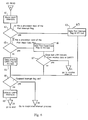
- Figs. 3-7 show the operation of the devices in Fig. 2 as this invention is utilized for efficiently interfacing an eight bit I/O UART to a thirty-two bit computer I/O bus.
- the decision blocks 31-33 of Fig. 3 represent the three conditions under which the UART Control Logic 12 of Fig. 2 responds to the UARTs 0-N or the Host Computer I/O Bus 21 in Fig. 2.
- Fig. 3 at 31 assume that one of the UARTs 0-N has issued an interrupt. The operation then proceeds to the interrupt service routine depicted in Fig. 4.
- the I/O Bus Control Logic 17 is enabled to block I/O accesses from or to the thirty-two bit I/O Bus 21 of the host computer from interfering with the current process.
- the identifier presently resident in the UART Identification Register 16 is latched to enable the logic to know which of the UARTs 0-N is issuing the interrupt.
- the UART Control Logic 12 reads the interrupt identification register of the particular UART whose identifier is currently latched in the UART ID Register 16.
- the contents of the UART interrupt instruction register tell the logic what type of UART interrupt is pending, such as "transmit holding register empty", "modem status", or a "receive" type interrupt, as described in detail below. These contents are then gated to the proper segment of the Port Interrupt Register 18.
- the contents of the UART ID Register 16 are gated to the proper segment of the Port Interrupt Register 18.
- a test is made by the UART Control Logic 12 to determine if an I/O write from the host computer bus is pending. If so, a flag is set at 44 to suspend this UART interrupt process to prevent undue delay in the host computer's I/O write from its data bus. Assuming at 43 that an I/O write is not pending, at 45 a test is made to determine if an I/O read is pending. If so, at 46 a flag is set to suspend the interrupt process to allow the host computer to proceed immediately with reading data from the UART and bus expansion circuit so as not to delay the host computer. Assuming that an I/O read was not pending at 45, at 47 a test is made to determine if the UART interrupt is a receive type interrupt.
- the UART Control Logic 12 Assuming that the UART interrupt is not a receive type interrupt, at 48 the UART Control Logic 12 generates a processor interrupt which is conveyed back to the thirty-two bit Host Computer I/O Bus 21. Thereafter, at 49 I/O reads and writes can be unblocked by the I/O Bus Control Logic 17.
- the line status register of the UART is again read and its contents are gated to the proper segment of the Port Read Data Register 19.
- the UART receive buffer is again read and its contents are gated to the proper segment of the Port Read Data Register 19.
- the Port Read Data Register 19 now contains thirty-two bits.
- an interrupt is issued to the host computer's thirty-two bit I/O Bus 21 and at 56 I/O reads and writes are unblocked by the I/O Bus Control Logic 17. Thereafter, the operation proceeds back to the three decisions of Fig. 3.
- the UART Control Logic 12 blocks any UART interrupts from further affecting the I/O bus expansion circuit.
- a test is made to determine if this I/O read from the host computer is a system read of the Port Interrupt Register 18. If so, the contents of the Port Interrupt Register 18 are gated to the host computer's thirty-two bit I/O Bus 21 through the I/O Bus Data Drivers and Receivers 24. If the I/O read is not a request for a system read of the Port Interrupt Register 18, at 64 the specific UART register is gated from the UART to the I/O Bus 21.
- an alternative to a system read of the Port Interrupt Register 18 (block 63) or a read of a specific UART register (block 64) is a system read of the Port Read Data Register 19. If this service is requested at block 65, the operation proceeds to 66 at which point the contents of the Port Read Data Register 19 are gated through the I/O Bus Data Drivers and Receivers 24 to the Host Computer thirty-two bit I/O Bus 21. If, however, the last UART line status register indicates that there is more received data in the UART, at 67 after gating the contents of the Port Read Data Register 19 to the host computer, the operation jumps to the handling of the receive interrupt which was described above in Fig. 5.
- the request from the host computer system was not to write data to the Port Write Data Register 20 but, instead, was a request to write directly to a UART (e.g., a control byte)
- a UART e.g., a control byte
- the proper UART is selected by the UART Control Logic 12 and at 74 the data is gated directly to the UART.
- the UART interrupts, blocked at 71, are unblocked and the operation proceeds back to Fig. 3 to await further UART interrupts or I/O read or write requests.
- an I/O bus expansion interface technique has been shown to enable an I/O device having an n-bit data bus to be interfaced to an m times n-bit I/O data bus of a host processor.
- the I/O bus expansion circuit disclosed herein is an interface which maximizes the computer processor's performance by providing full I/O data bus bandwidth and allowing overlap of processor execution and I/O bus expansion interface circuit operation. This is accomplished by: 1) prefetching multiple control and/or data fields from the I/O device and presenting that information to the host without delay and 2) burst writing multiple bytes from the host to the bus expansion interface circuit, without delay of the host, and thereafter making these bytes individually available to the I/O device.
Abstract
Description
- This invention relates to data processing system interfaces in general, and more particularly to an arrangement for interfacing a device having an n-bit Input/Output data bus to an m x n-bit I/O data bus.
- Today's processor development is far exceeding the development of I/O device support. It is common place now for personal, mini and micro computers to have thirty-two bit processor units that can execute instructions in the tens of nanoseconds and have I/O data bus widths of thirty-two bits, while only recently such processors had executed instructions in tens of microseconds and had I/O data bus widths of eight bits. The I/O device technology, however, is developing at a much slower pace. Because optimal utilization of these new high performance processors is highly I/O intensive (i.e., they spend much of their time accessing disks, communication ports, etc.) users have often not been able to realize the full potential of their processing power due to the low bandwidth of their I/O buses.
- Many of the available I/O devices for use with state of the art computers do not fully exploit the bandwidth of the I/O buses supported by their processors. As the processor technology has rapidly progressed from eight bit I/O buses to sixteen bits and now thirty-two bit data buses, the peripheral device development support has been much slower such that many of these devices still provide only eight bit data buses.
- One of the reasons for the slower device development has been the cost of the I/O devices themselves. Another reason has been the packaging of these devices, due to the larger data bus pin out required.
- By way of example, no present Universal Asynchronous Receiver/Transmitter (UART) exists which has a thirty-two bit I/O bus, although there is a real need for such a device to fully utilize the potential of the newest processors which have thirty-two bit I/O buses. The traditional solution to this problem has been to effectively operate the processor as if it, too, was limited to an eight bit bus while it communicated with the eight bit UART. The performance compromises involved with this solution are well understood.
- It would, therefore, be of great benefit to have the capability to interface the newer processors having wider buses to the existing I/O devices having narrower buses while operating the processor as if it were communicating with an I/O device having a bus width equal to its own.
- According to the invention, there is provided an interface circuit for transferring data between a processor having an n x m bit processor data bus and an input/output device having an n bit input/output data bus comprising a register system for temporarily storing a group of fields of data and control logic means operable to prefetch a group of said fields, a field at a time, from the n bit input/output data bus, to store the group in the register system, and to transfer the stored group from the register system to the processor data bus in a single read by the processor.
- In an embodiment of the invention, to be detailed later, an I/O bus expansion interface technique is disclosed which enables an I/O device having an n-bit data bus to be interfaced to an m times n-bit I/O data bus of a host processor. This I/O bus expansion circuit is an interface which maximizes the computer processor's performance by providing full I/O data bus bandwidth and allowing overlap of processor execution and I/O bus expansion interface circuit operation. This is accomplished by: 1) prefetching multiple control and/or data fields from the I/O device and presenting that information to the host without delay and 2) burst writing multiple fields from the host to the bus expansion interface circuit, without delay of the host, and thereafter making these fields individually available to the I/O device.
- The bus expansion circuit is composed of a set of registers and control logic with which a host computer communicates through the m times n-bit I/O bus associated with the host computer. This bus expansion circuit then communicates with the n-bit bus of the external I/O device, such as a UART. The processor writes out as much as m times n bits to a write register in one operation. Then, in a succession of operations of the bus expansion circuit, n-bit portions of this data is communicated to the external I/O device. As a complement of this operation, the control logic of the bus expansion circuit is able to load an m times n bit wide read register through a succession of n-bit reads of the I/O device so that the host computer processor can then execute a single read operation to read the m times n bits. The control logic is further operable to allow direct host computer to I/O device communication for transfer of I/O device control information of less than m times n bits.
- Accordingly, the system provides a simple means to multiplex data and control information from a device having an n-bit (e.g., eight bit) I/O bus onto a processor's I/O data bus which can be any multiple of n bits wide, for example, thirty-two bits. This I/O bus expansion circuit provides an inexpensive yet effective means to gain back the I/O bus bandwidth for processors with data buses that are larger than n bits. The circuit may be used on the processor boards, on nonintelligent adapters and on intelligent adapters which also contain processors with I/O data buses greater than n bits. For example, the circuit can be used with eight bit UARTs, eight bit diskette controllers, eight bit hard file controllers, and eight bit time-of-day clocks which provide multiple bytes of data, as well as floating point math processors.
- The embodiment will now be described in detail with reference to the accompany drawings, in which:
- Fig. 1 is a block diagram of the I/O bus expansion circuit embodying the invention;
- Fig. 2 is an implementation of the bus expansion circuit in which an eight bit UART is interfaced to a 32 bit computer I/O data bus;
- Figs. 3-7 are flow diagrams of the operation of the devices in Fig. 2 for efficiently interfacing a UART having an eight bit I/O data bus to a thirty-two bit computer I/O data bus.
- Referring now to Fig. 1, one or more I/
O devices Interface Registers Bus Expansion Circuit 20 of this invention. As will be described in detail below, the registers 3-5 communicate with a host computer's I/O Data Bus 8 which may be m times n bits wide. Also contained within the I/OBus Expansion Circuit 20 is an I/O Address and Control Decode Logic Unit 7 which communicates with the host computer's I/O Address Bus 9, as described below. The I/O devices Interface registers Control Logic Unit 6. - The width of the
Interface Registers O Data Bus 8. Each register is composed of n-bit segments which are separately gatable within the Bus Expansion Circuit. These registers may be gated to or from the I/O Data Bus 8 at the full width of theData Bus 8. Each of these registers is uniquely addressable by the I/O bus. - A Device Interrupt Interface Register 3 is loaded by the Device
Control Logic Unit 6 when a device requires service. The format of this register is both device and data bus width dependent. The purpose of this register is to allow the Bus Expansion Circuit to gate additional data to the I/O data bus than simply the device n-bit service request. In the case in which an n-bit UART is one of devices 1-2, this register contains an identifier of the UART requesting service and the actual service request as read by the DeviceControl Logic Unit 6 from the UART. - A Device Read
Data Interface Register 4 is loaded by the DeviceControl Logic Unit 6 when a device service request indicates that there is data available for the processor. The DeviceControl Logic Unit 6 will automatically read the data from the device and gate the data into the proper n-bit segment of this register before interrupting the processor with the service request. - It is possible that this Device
Read Data Register 4 can be duplicated multiple times for a particular implementation. For example, if the device is capable of buffering or fetching more than one times the I/O data bus width then it may be advantageous to have more than one Device Read Data Register all of which are separately addressable from the I/O bus. - This feature of the I/O Bus Expansion Circuit 10 is to have the data available at the time of the processor interrupt and not cause the processor or I/O bus to wait for the data. It also provides for full utilization of the I/O bus bandwidth on read operations. An additional feature that is provided in this generalized example is that the Device
Control Logic Unit 6 can prefetch more data from the I/O device - There are multiple addresses to the Device Write
Data Interface Register 5. The number of these addresses is dependent on the number of devices being supported and the width of the two data buses. In the example of an n-bit device device Data Write Register 5. One of the addresses to these registers indicates a four byte write, a second of the addresses indicates a three byte write, another of the addresses indicates a two byte write and a fourth of these addresses indicates a one byte write. - The Device
Control Logic Unit 6 gates the I/O bus to the appropriate DeviceWrite Data Register 5 address when it decodes an I/O bus write operation. It can then gate the proper number of data bytes to the n-bit device. This feature allows the host processor to fully utilize the I/O bus bandwidth for write operations and allows the DeviceControl Logic Unit 6 to gate the data in one byte operations to the device while the processor is left free to do additional work. - The Device Control
Logic Unit 6 provides the necessary function to respond to interrupts from thedevices O buses 8 and 9. - When the
device Control Logic Unit 6 reads the service request from the device and gates it and additional data as required to the Device Interrupt Register 3. It then may optionally interrupt the processor depending on the type of service request made by the device. - When the Device
Control Logic Unit 6 is notified by the Address and Control Decode Logic Unit 7 that the WriteData Register 5 has been written it then moves this data from the register to the device. - When the
device Data Register 4. This feature allows the I/O Bus Expansion Circuit to work asynchronously with the processor. The Device ControlLogic Unit 6 also provides the synchronization between the two I/O data buses to insure that no data is lost. - The Address and Control Decode Logic Unit 7 provides the necessary controls to gate data to the Write
Data Register 5 during I/O write operations. It also provides the logic to gate theRead Data Register 4 and Device Interrupt Register 3 to the I/O data bus for host processor read operations. - Fig. 2 shows an implementation of the I/O Bus Expansion Circuit for interfacing a National Semiconductor eight bit UART, part number NS16550A to a 32 bit I/O data bus. Those skilled in art will recognize that while a particular eight bit UART has been chosen for this example, the invention taught and claimed herein may be utilized to interface any of a multitude of other devices having n-bit I/O buses to other buses which are m times n bits wide. In this implementation the device control logic consists of
UART Control Logic 12, a 32 bit to 8 bit Multiplexor (MPX) 14 and aUART ID Register 16. - This implementation converts the UART's Interrupt Identification Register, Line Status Register and Receiver Buffer and Transmit Holding Register data from the UART's eight bit bus to the host processor's thirty-two bit bus.
- The functions of the
UART Control Logic 12 are to: 1) select the UART 0-N to be serviced, 2) gate the data to and from the 8 bit bus to the proper segment of a PortRead Data Register 19 and aWrite Data Register 20 by directing themultiplexor 14, 3) sense the UART interrupt lines and interpret the contents of the Interrupt Identification Register, and create an interrupt to the host processor when the proper conditions have been met. - The
UART ID Register 16 provides the mechanism to latch up the ID of the current UART that is being serviced. It also provides the priority selection of UART's in the case that multiple UART's request service at the same time. - The Port Interrupt
Register 18 is a single thirty-two bit wide register that is loaded by theUART Control Logic 12 with: 1) the contents of the UART ID Register 16 (two bytes) and 2) the contents of the Interrupt Identification Register from the UART which requires service. - The Port
Read Data Register 19 is a single thirty-two bit wide register to which the contents of the Receiver Buffer and Line Status Registers for the UART requiring receive data service are gated. - There is only one physical Port
Write Data Register 20 per UART; however it can be addressed four times for each UART that is installed. The four addresses per UART are used to to inform theUART Control Logic 12 of the number of valid bytes of data that were placed on the I/O bus. For example, address x indicates that four bytes of data were placed on the I/O bus, address x+1 indicates that three bytes of data were placed on the I/O bus, address x+2 indicates that two bytes of data were placed on the I/O bus, and address x+3 indicates that one byte of data was placed on the I/O bus. - The I/O Address and
Control Decode Logic 17 decodes the I/O read and write control lines and gates data to or from the selected register and decodes the I/O addresses to select the proper register. - Reference is now made to the flow diagrams of Figs. 3-7 which show the operation of the devices in Fig. 2 as this invention is utilized for efficiently interfacing an eight bit I/O UART to a thirty-two bit computer I/O bus. The decision blocks 31-33 of Fig. 3 represent the three conditions under which the
UART Control Logic 12 of Fig. 2 responds to the UARTs 0-N or the Host Computer I/O Bus 21 in Fig. 2. In Fig. 3 at 31, assume that one of the UARTs 0-N has issued an interrupt. The operation then proceeds to the interrupt service routine depicted in Fig. 4. - In Fig. 4 at 40 the I/O
Bus Control Logic 17 is enabled to block I/O accesses from or to the thirty-two bit I/O Bus 21 of the host computer from interfering with the current process. Concurrently, the identifier presently resident in theUART Identification Register 16 is latched to enable the logic to know which of the UARTs 0-N is issuing the interrupt. At 41, theUART Control Logic 12 reads the interrupt identification register of the particular UART whose identifier is currently latched in theUART ID Register 16. The contents of the UART interrupt instruction register tell the logic what type of UART interrupt is pending, such as "transmit holding register empty", "modem status", or a "receive" type interrupt, as described in detail below. These contents are then gated to the proper segment of the Port InterruptRegister 18. At 42 the contents of theUART ID Register 16 are gated to the proper segment of the Port InterruptRegister 18. - At 43 a test is made by the
UART Control Logic 12 to determine if an I/O write from the host computer bus is pending. If so, a flag is set at 44 to suspend this UART interrupt process to prevent undue delay in the host computer's I/O write from its data bus. Assuming at 43 that an I/O write is not pending, at 45 a test is made to determine if an I/O read is pending. If so, at 46 a flag is set to suspend the interrupt process to allow the host computer to proceed immediately with reading data from the UART and bus expansion circuit so as not to delay the host computer. Assuming that an I/O read was not pending at 45, at 47 a test is made to determine if the UART interrupt is a receive type interrupt. Assuming that the UART interrupt is not a receive type interrupt, at 48 theUART Control Logic 12 generates a processor interrupt which is conveyed back to the thirty-two bit Host Computer I/O Bus 21. Thereafter, at 49 I/O reads and writes can be unblocked by the I/OBus Control Logic 17. - Assume now that at 47 the UART interrupt was a receive type interrupt. "Receive line status", "receive data available", and "character timeout" are examples of receive type interrupts. The operation then proceeds as described in the flow chart of Fig. 5. At
block 51 the contents of the line status register of the UART are read and gated to the proper segment of the PortRead Data Register 19. The contents of the line status register comprise eight bits. The UART address for this operation is known from the contents of theUART ID Register 16. At 52, the contents of the UART receive buffer are read and gated to the proper segment of the PortRead Data Register 19. This operation loads an eight bit data byte into the PortRead Data Register 19. At 53 the line status register of the UART is again read and its contents are gated to the proper segment of the PortRead Data Register 19. At 54 the UART receive buffer is again read and its contents are gated to the proper segment of the PortRead Data Register 19. The PortRead Data Register 19 now contains thirty-two bits. Atblock 55 an interrupt is issued to the host computer's thirty-two bit I/O Bus 21 and at 56 I/O reads and writes are unblocked by the I/OBus Control Logic 17. Thereafter, the operation proceeds back to the three decisions of Fig. 3. - In Fig. 3, assume now that at
block 32 an I/O read is detected which indicates that the host processor is ready to read data from the bus expansion circuit. The operation then proceeds to the flow chart of Fig. 6. - In Fig. 6, when an I/O read is detected, at 61 the
UART Control Logic 12 blocks any UART interrupts from further affecting the I/O bus expansion circuit. At 62 a test is made to determine if this I/O read from the host computer is a system read of the Port InterruptRegister 18. If so, the contents of the Port InterruptRegister 18 are gated to the host computer's thirty-two bit I/O Bus 21 through the I/O Bus Data Drivers andReceivers 24. If the I/O read is not a request for a system read of the Port InterruptRegister 18, at 64 the specific UART register is gated from the UART to the I/O Bus 21. At 68, if this I/O read occurs during the suspension of the servicing of a UART interrupt (block 46, Fig. 4), the operation proceeds back to block 47, Fig. 4 to resume the servicing of the UART interrupt. Otherwise, the operation proceeds to 69 to re-enable theUART Control Logic 12 to receive UART interrupts which were previously blocked at 61, at the beginning of the I/O read service. - In the I/O read operation of Fig. 6, an alternative to a system read of the Port Interrupt Register 18 (block 63) or a read of a specific UART register (block 64) is a system read of the Port
Read Data Register 19. If this service is requested atblock 65, the operation proceeds to 66 at which point the contents of the PortRead Data Register 19 are gated through the I/O Bus Data Drivers andReceivers 24 to the Host Computer thirty-two bit I/O Bus 21. If, however, the last UART line status register indicates that there is more received data in the UART, at 67 after gating the contents of the PortRead Data Register 19 to the host computer, the operation jumps to the handling of the receive interrupt which was described above in Fig. 5. - Referring back to Fig. 3, if an I/O write is detected at 33, indicating that the host computer is ready to write data out to a UART, the operation proceeds to 71, Fig. 7, wherein further UART interrupts are blocked by the
UART Control Logic 12 from entering the bus expansion circuit. At 72, if the host system is requesting to write data to the PortWrite Data Register 20, the appropriate Port Write Data Register is selected at 75. At 76, the data is gated from the host computer to the selected PortWrite Data Register 20 and at 77 the proper number of bytes (depending on the selected address at 75 to which the data was gated at 76) is gated from the PortWrite Data Register 20 to the selected UART. Thereafter, the UART interrupts blocked at 71 are unblocked at 78. If, at 72 the request from the host computer system was not to write data to the PortWrite Data Register 20 but, instead, was a request to write directly to a UART (e.g., a control byte), then at 73 the proper UART is selected by theUART Control Logic 12 and at 74 the data is gated directly to the UART. Thereafter, at 78 the UART interrupts, blocked at 71, are unblocked and the operation proceeds back to Fig. 3 to await further UART interrupts or I/O read or write requests. - In summary, an I/O bus expansion interface technique has been shown to enable an I/O device having an n-bit data bus to be interfaced to an m times n-bit I/O data bus of a host processor. The I/O bus expansion circuit disclosed herein is an interface which maximizes the computer processor's performance by providing full I/O data bus bandwidth and allowing overlap of processor execution and I/O bus expansion interface circuit operation. This is accomplished by: 1) prefetching multiple control and/or data fields from the I/O device and presenting that information to the host without delay and 2) burst writing multiple bytes from the host to the bus expansion interface circuit, without delay of the host, and thereafter making these bytes individually available to the I/O device.
Claims (7)
prefetching a group of fields, a group at a time, from the input/output device along the n bit data bus;
storing said fields in a register system; and
transferring said fields, in a single operation, to the processor along the m x n bit data bus.
transferring a group of fields of data simultaneously from the processors to the register system along the m x n data bus;
storing the transferred group in the register system; and
transferring the group, a field at a time, from the register system to the input/output device along the n bit data bus.
Applications Claiming Priority (2)
| Application Number | Priority Date | Filing Date | Title |
|---|---|---|---|
| US07/149,796 US5014236A (en) | 1988-01-29 | 1988-01-29 | Input/output bus expansion interface |
| US149796 | 1988-01-29 |
Publications (3)
| Publication Number | Publication Date |
|---|---|
| EP0325856A2 true EP0325856A2 (en) | 1989-08-02 |
| EP0325856A3 EP0325856A3 (en) | 1990-07-18 |
| EP0325856B1 EP0325856B1 (en) | 1996-05-15 |
Family
ID=22531834
Family Applications (1)
| Application Number | Title | Priority Date | Filing Date |
|---|---|---|---|
| EP88311904A Expired - Lifetime EP0325856B1 (en) | 1988-01-29 | 1988-12-16 | Interface circuit for data transfer between processor and input/output device |
Country Status (6)
| Country | Link |
|---|---|
| US (1) | US5014236A (en) |
| EP (1) | EP0325856B1 (en) |
| JP (1) | JPH01197866A (en) |
| AR (1) | AR245302A1 (en) |
| BR (1) | BR8900343A (en) |
| DE (1) | DE3855300T2 (en) |
Cited By (6)
| Publication number | Priority date | Publication date | Assignee | Title |
|---|---|---|---|---|
| EP0468823A2 (en) * | 1990-07-27 | 1992-01-29 | Dell Usa L.P. | Computer data routing system |
| EP0480417A2 (en) * | 1990-10-11 | 1992-04-15 | Lsi Logic Corporation | Memory control architecture for microprocessors |
| EP0482589A2 (en) * | 1990-10-22 | 1992-04-29 | Kabushiki Kaisha Toshiba | Method and apparatus for controlling bus in computer system to which expansion unit is connectable |
| EP0568329A1 (en) * | 1992-05-01 | 1993-11-03 | Advanced Micro Devices, Inc. | Peripheral memory buffer apparatus and method of using same |
| EP0639032A2 (en) * | 1993-08-09 | 1995-02-15 | C-Cube Microsystems, Inc. | Structure and method for a multistandard video encoder/decoder |
| US5910909A (en) * | 1995-08-28 | 1999-06-08 | C-Cube Microsystems, Inc. | Non-linear digital filters for interlaced video signals and method thereof |
Families Citing this family (15)
| Publication number | Priority date | Publication date | Assignee | Title |
|---|---|---|---|---|
| JPH04233059A (en) * | 1990-06-25 | 1992-08-21 | Internatl Business Mach Corp <Ibm> | Information processing apparatus |
| EP0518488A1 (en) * | 1991-06-12 | 1992-12-16 | Advanced Micro Devices, Inc. | Bus interface and processing system |
| US5274783A (en) * | 1991-06-28 | 1993-12-28 | Digital Equipment Corporation | SCSI interface employing bus extender and auxiliary bus |
| US5495594A (en) * | 1991-07-12 | 1996-02-27 | Zilog, Inc. | Technique for automatically adapting a peripheral integrated circuit for operation with a variety of microprocessor control signal protocols |
| US5229926A (en) * | 1992-04-01 | 1993-07-20 | Digital Equipment Corporation | Power supply interlock for a distributed power system |
| TW276312B (en) * | 1992-10-20 | 1996-05-21 | Cirrlis Logic Inc | |
| USH1507H (en) * | 1993-04-23 | 1995-12-05 | The United States Of America As Represented By The Secretary Of The Navy | Demand assigned multiple access (DAMA) device controller interface |
| US5721841A (en) * | 1994-11-04 | 1998-02-24 | Texas Instruments Incorporated | Adapter having data aligner including register being loaded to or from memory with an offset in accordance with predetermined network fragmentation parameters |
| JP3566364B2 (en) * | 1994-12-22 | 2004-09-15 | キヤノン株式会社 | Data processing apparatus and method |
| US5764927A (en) * | 1995-09-29 | 1998-06-09 | Allen Bradley Company, Inc. | Backplane data transfer technique for industrial automation controllers |
| US6002883A (en) * | 1996-07-18 | 1999-12-14 | International Business Machines Corporation | System with intersystem information links for intersystem traffic having I/O traffic being transmitted to and from processor bus via processor means |
| KR100291005B1 (en) | 1998-03-05 | 2001-07-12 | 윤종용 | Fan-out expansion circuit for multi-drop connection with rs-485 |
| US7020726B2 (en) * | 2001-05-24 | 2006-03-28 | Lsi Logic Corporation | Methods and apparatus for signaling to switch between different bus bandwidths |
| US7124222B2 (en) * | 2003-12-16 | 2006-10-17 | 1X1 Mobile, Ltd. | Control system and method for a communications interface |
| FR3015068B1 (en) * | 2013-12-18 | 2016-01-01 | Commissariat Energie Atomique | SIGNAL PROCESSING MODULE, IN PARTICULAR FOR NEURONAL NETWORK AND NEURONAL CIRCUIT |
Citations (1)
| Publication number | Priority date | Publication date | Assignee | Title |
|---|---|---|---|---|
| US4417303A (en) * | 1981-02-25 | 1983-11-22 | Leeds & Northrup Company | Multi-processor data communication bus structure |
Family Cites Families (5)
| Publication number | Priority date | Publication date | Assignee | Title |
|---|---|---|---|---|
| US3725864A (en) * | 1971-03-03 | 1973-04-03 | Ibm | Input/output control |
| US4447878A (en) * | 1978-05-30 | 1984-05-08 | Intel Corporation | Apparatus and method for providing byte and word compatible information transfers |
| US4716527A (en) * | 1984-12-10 | 1987-12-29 | Ing. C. Olivetti | Bus converter |
| US4727477A (en) * | 1985-03-22 | 1988-02-23 | International Business Machines Corp. | Logically transportable microprocessor interface control unit permitting bus transfers with different but compatible other microprocessors |
| JPS61265653A (en) * | 1985-05-20 | 1986-11-25 | Fujitsu Ltd | Direct memory access system |
-
1988
- 1988-01-29 US US07/149,796 patent/US5014236A/en not_active Expired - Fee Related
- 1988-11-19 JP JP63291124A patent/JPH01197866A/en active Pending
- 1988-12-16 DE DE3855300T patent/DE3855300T2/en not_active Expired - Fee Related
- 1988-12-16 EP EP88311904A patent/EP0325856B1/en not_active Expired - Lifetime
-
1989
- 1989-01-24 AR AR89313058A patent/AR245302A1/en active
- 1989-01-27 BR BR898900343A patent/BR8900343A/en not_active Application Discontinuation
Patent Citations (1)
| Publication number | Priority date | Publication date | Assignee | Title |
|---|---|---|---|---|
| US4417303A (en) * | 1981-02-25 | 1983-11-22 | Leeds & Northrup Company | Multi-processor data communication bus structure |
Non-Patent Citations (3)
| Title |
|---|
| IBM TECHNICAL DISCLOSURE BULLETIN. vol. 14, no. 3, August 1971, NEW YORK US pages 799 - 800; R.A. Palm et al.: "I/O channel for computer" * |
| IBM TECHNICAL DISCLOSURE BULLETIN. vol. 26, no. 10A, March 1984, NEW YORK US pages 5199 - 5206; S.E.Edick: "Direct memory access controller" * |
| IBM TECHNICAL DISCLOSURE BULLETIN. vol. 30, no. 6, November 1987, NEW YORK US pages 205 - 207; "Eight-bit to sixteen-bit memory converter" * |
Cited By (16)
| Publication number | Priority date | Publication date | Assignee | Title |
|---|---|---|---|---|
| EP0468823A2 (en) * | 1990-07-27 | 1992-01-29 | Dell Usa L.P. | Computer data routing system |
| EP0468823A3 (en) * | 1990-07-27 | 1992-09-30 | Dell Usa Corporation | Computer data routing system |
| EP0480417A3 (en) * | 1990-10-11 | 1994-05-18 | Lsi Logic Corp | Memory control architecture for microprocessors |
| EP0480417A2 (en) * | 1990-10-11 | 1992-04-15 | Lsi Logic Corporation | Memory control architecture for microprocessors |
| US5454084A (en) * | 1990-10-22 | 1995-09-26 | Kabushiki Kaisha Toshiba | Method and apparatus for controlling bus in computer system to which expansion unit is connectable |
| EP0482589A3 (en) * | 1990-10-22 | 1992-11-25 | Kabushiki Kaisha Toshiba | Method and apparatus for controlling bus in computer system to which expansion unit is connectable |
| EP0482589A2 (en) * | 1990-10-22 | 1992-04-29 | Kabushiki Kaisha Toshiba | Method and apparatus for controlling bus in computer system to which expansion unit is connectable |
| EP0568329A1 (en) * | 1992-05-01 | 1993-11-03 | Advanced Micro Devices, Inc. | Peripheral memory buffer apparatus and method of using same |
| EP0639032A2 (en) * | 1993-08-09 | 1995-02-15 | C-Cube Microsystems, Inc. | Structure and method for a multistandard video encoder/decoder |
| EP0639032A3 (en) * | 1993-08-09 | 1995-11-29 | C Cube Microsystems | Structure and method for a multistandard video encoder/decoder. |
| US5598514A (en) * | 1993-08-09 | 1997-01-28 | C-Cube Microsystems | Structure and method for a multistandard video encoder/decoder |
| US5630033A (en) * | 1993-08-09 | 1997-05-13 | C-Cube Microsystems, Inc. | Adaptic threshold filter and method thereof |
| US5740340A (en) * | 1993-08-09 | 1998-04-14 | C-Cube Microsystems, Inc. | 2-dimensional memory allowing access both as rows of data words and columns of data words |
| US6071004A (en) * | 1993-08-09 | 2000-06-06 | C-Cube Microsystems, Inc. | Non-linear digital filters for interlaced video signals and method thereof |
| US6122442A (en) * | 1993-08-09 | 2000-09-19 | C-Cube Microsystems, Inc. | Structure and method for motion estimation of a digital image by matching derived scores |
| US5910909A (en) * | 1995-08-28 | 1999-06-08 | C-Cube Microsystems, Inc. | Non-linear digital filters for interlaced video signals and method thereof |
Also Published As
| Publication number | Publication date |
|---|---|
| EP0325856A3 (en) | 1990-07-18 |
| BR8900343A (en) | 1989-09-19 |
| AR245302A1 (en) | 1993-12-30 |
| JPH01197866A (en) | 1989-08-09 |
| US5014236A (en) | 1991-05-07 |
| DE3855300D1 (en) | 1996-06-20 |
| EP0325856B1 (en) | 1996-05-15 |
| DE3855300T2 (en) | 1996-11-21 |
Similar Documents
| Publication | Publication Date | Title |
|---|---|---|
| EP0325856B1 (en) | Interface circuit for data transfer between processor and input/output device | |
| US5444853A (en) | System and method for transferring data between a plurality of virtual FIFO's and a peripheral via a hardware FIFO and selectively updating control information associated with the virtual FIFO's | |
| EP0080891B1 (en) | Direct memory access logic system for a data transfer network | |
| EP0489504B1 (en) | Bidirectional FIFO buffer for interfacing between two buses | |
| US6334162B1 (en) | Efficient data transfer mechanism for input/out devices having a device driver generating a descriptor queue and monitoring a status queue | |
| US5918028A (en) | Apparatus and method for smart host bus adapter for personal computer cards | |
| US4860244A (en) | Buffer system for input/output portion of digital data processing system | |
| US4419728A (en) | Channel interface circuit providing virtual channel number translation and direct memory access | |
| EP0080890B1 (en) | Interface circuit for subsystem controller | |
| EP0432978A2 (en) | Apparatus for conditioning priority arbitration in buffered direct memory addressing | |
| EP0485507B1 (en) | Modular input/output system for supercomputers | |
| US5859990A (en) | System for transferring data segments from a first storage device to a second storage device using an alignment stage including even and odd temporary devices | |
| US5678064A (en) | Local bus-ISA bridge for supporting PIO and third party DMA data transfers to IDE drives | |
| KR100309189B1 (en) | System input/output interface design for scaling | |
| US4456970A (en) | Interrupt system for peripheral controller | |
| US6070204A (en) | Method and apparatus for using universal serial bus keyboard to control DOS operations | |
| US6105080A (en) | Host adapter DMA controller with automated host reply capability | |
| EP0074704B1 (en) | Subsystem controller | |
| JPS61855A (en) | Processor interface circuit | |
| EP0139254A2 (en) | Apparatus and method for direct memory to peripheral and peripheral to memory data transfer | |
| EP0618537B1 (en) | System and method for interleaving status information with data transfers in a communications adapter | |
| KR20030048415A (en) | Streamlining ata device initialization | |
| US6877060B2 (en) | Dynamic delayed transaction buffer configuration based on bus frequency | |
| US5129065A (en) | Apparatus and methods for interface register handshake for controlling devices | |
| EP0118669A2 (en) | Channel subsystem |
Legal Events
| Date | Code | Title | Description |
|---|---|---|---|
| PUAI | Public reference made under article 153(3) epc to a published international application that has entered the european phase |
Free format text: ORIGINAL CODE: 0009012 |
|
| AK | Designated contracting states |
Kind code of ref document: A2 Designated state(s): DE FR GB |
|
| 17P | Request for examination filed |
Effective date: 19891117 |
|
| PUAL | Search report despatched |
Free format text: ORIGINAL CODE: 0009013 |
|
| AK | Designated contracting states |
Kind code of ref document: A3 Designated state(s): DE FR GB |
|
| 17Q | First examination report despatched |
Effective date: 19930302 |
|
| GRAH | Despatch of communication of intention to grant a patent |
Free format text: ORIGINAL CODE: EPIDOS IGRA |
|
| GRAA | (expected) grant |
Free format text: ORIGINAL CODE: 0009210 |
|
| AK | Designated contracting states |
Kind code of ref document: B1 Designated state(s): DE FR GB |
|
| REF | Corresponds to: |
Ref document number: 3855300 Country of ref document: DE Date of ref document: 19960620 |
|
| ET | Fr: translation filed | ||
| PGFP | Annual fee paid to national office [announced via postgrant information from national office to epo] |
Ref country code: GB Payment date: 19961126 Year of fee payment: 9 |
|
| PGFP | Annual fee paid to national office [announced via postgrant information from national office to epo] |
Ref country code: DE Payment date: 19970116 Year of fee payment: 9 |
|
| PLBE | No opposition filed within time limit |
Free format text: ORIGINAL CODE: 0009261 |
|
| STAA | Information on the status of an ep patent application or granted ep patent |
Free format text: STATUS: NO OPPOSITION FILED WITHIN TIME LIMIT |
|
| 26N | No opposition filed | ||
| PG25 | Lapsed in a contracting state [announced via postgrant information from national office to epo] |
Ref country code: FR Effective date: 19970829 |
|
| REG | Reference to a national code |
Ref country code: FR Ref legal event code: ST |
|
| PG25 | Lapsed in a contracting state [announced via postgrant information from national office to epo] |
Ref country code: GB Free format text: LAPSE BECAUSE OF NON-PAYMENT OF DUE FEES Effective date: 19971216 |
|
| GBPC | Gb: european patent ceased through non-payment of renewal fee |
Effective date: 19971216 |
|
| PG25 | Lapsed in a contracting state [announced via postgrant information from national office to epo] |
Ref country code: DE Free format text: LAPSE BECAUSE OF NON-PAYMENT OF DUE FEES Effective date: 19980901 |