EP0322483A1 - Standortsanzeige eines Datenelementes - Google Patents
Standortsanzeige eines Datenelementes Download PDFInfo
- Publication number
- EP0322483A1 EP0322483A1 EP87202504A EP87202504A EP0322483A1 EP 0322483 A1 EP0322483 A1 EP 0322483A1 EP 87202504 A EP87202504 A EP 87202504A EP 87202504 A EP87202504 A EP 87202504A EP 0322483 A1 EP0322483 A1 EP 0322483A1
- Authority
- EP
- European Patent Office
- Prior art keywords
- sequence
- input
- data
- output
- coupled
- Prior art date
- Legal status (The legal status is an assumption and is not a legal conclusion. Google has not performed a legal analysis and makes no representation as to the accuracy of the status listed.)
- Withdrawn
Links
Images

Classifications
-
- G—PHYSICS
- G06—COMPUTING OR CALCULATING; COUNTING
- G06F—ELECTRIC DIGITAL DATA PROCESSING
- G06F1/00—Details not covered by groups G06F3/00 - G06F13/00 and G06F21/00
- G06F1/02—Digital function generators
-
- G—PHYSICS
- G01—MEASURING; TESTING
- G01S—RADIO DIRECTION-FINDING; RADIO NAVIGATION; DETERMINING DISTANCE OR VELOCITY BY USE OF RADIO WAVES; LOCATING OR PRESENCE-DETECTING BY USE OF THE REFLECTION OR RERADIATION OF RADIO WAVES; ANALOGOUS ARRANGEMENTS USING OTHER WAVES
- G01S3/00—Direction-finders for determining the direction from which infrasonic, sonic, ultrasonic, or electromagnetic waves, or particle emission, not having a directional significance, are being received
- G01S3/02—Direction-finders for determining the direction from which infrasonic, sonic, ultrasonic, or electromagnetic waves, or particle emission, not having a directional significance, are being received using radio waves
- G01S3/14—Systems for determining direction or deviation from predetermined direction
- G01S3/38—Systems for determining direction or deviation from predetermined direction using adjustment of real or effective orientation of directivity characteristic of an antenna or an antenna system to give a desired condition of signal derived from that antenna or antenna system, e.g. to give a maximum or minimum signal
Definitions
- This invention relates to a method of generating a signal indicative of the position, within a sequence of data elements of first and second kinds, of that element or pair of elements which lies at the centre of the or each largest group of elements of the first kind.
- the invention also relates to apparatus for carrying out such a method.
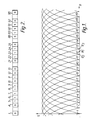
- the antenna has multiple feeds which form a large number of overlapping reception beams which give multidirectional (possibly even omnidirectional) coverage.
- the sensitivity S of the antenna as a function of direction O may be of the form illustrated in Fig.
- the invention provides a method of generating a signal indicative of the position, within a sequence of data elements of first and second kinds, of that element or pair of elements which lies at the centre of the or each largest group of elements of the first kind, said method comprising the step of changing each element of the first kind which has an element of the second kind as an immediate neighbour in the sequence into an element of the second kind, repeating said step until all elements of the sequence are of the second kind, and generating a signal indicative of the position(s) of the element(s) of the first kind present immediately before the carrying out of that said step which results in all elements of the sequence being of the second kind.
- the sequence of Fig. 2 is in fact derived from the output feeds of a multibeam radio antenna and the feed or associated circuitry corresponding to for example bit 10 becomes faulty so that this bit is a "0" whereas it should be a "1", an erroneous result will be obtained on carrying out the method so far defined.
- the aforesaid sequence may be formed from an initial sequence of data elements of said first and second kinds by changing each element of said initial sequence which is of the second kind and which has an element of the first kind as an immediate neighbour in said initial sequence into an element of the first kind. If the initial sequence is, for example, that shown in Fig.
- bits 4, 10, 13, 21, 25, 88 and 92 being changed into a "1". This can be referred to as "1-spreading". If the resulting sequence is then subjected to 1-stripping operations as previously set forth eventually only bits 8 and 9 will be "1", as required.
- the 1-stripping operations can be conveniently carried out by means of apparatus comprising first storage means for said sequence, which storage means has a storage location corresponding to each said data element and also a clock signal input, a data input corresponding to each of said data elements, which input is coupled to an input of the corresponding storage location, a logic gate corresponding to each pair of alternate elements in said sequence, which gate has inputs coupled to outputs of the storage locations corresponding to the elements of the relevant pair and is constructed to generate at an output thereof a signal indicative of whether data elements stored in the storage locations corresponding to the elements of the relevant pair are both of the first kind, which output is coupled to an input of the storage location corresponding to the element which lies within the sequence between the elements of the relevant pair, second storage means having a storage location corresponding to each storage location of the first storage means and also a clock signal input, a coupling from an output of each storage location of the first storage means to an input of the corresponding storage location of the second storage means, a clock signal generator circuit having an inhibit signal input and clock signal outputs coupled
- Each storage location of the first storage means may comprise a respective J-K function flip-flop, the said logic gate which has an output coupled to an input thereof having its output coupled to the K-function input thereof and the corresponding data input being coupled to the J-function input thereof via a further logic gate, these further logic gates having control inputs coupled to a control signal output of said clock pulse generator circuit and said clock pulse generator circuit being arranged to apply a control signal to said control signal output for blocking said further logic gates when a sequence of data elements presented to said data inputs has been stored in said J-K function flip-flops.
- a priority encoder may be provided having an input corresponding to and coupled to an output of each storage location of the second storage means, which encoder is constructed to generate a number in binary form corresponding to the first position in the sequence for which the corresponding storage location of the second storage means is storing a data element of the first kind.
- the apparatus may include an auxiliary logic gate corresponding to each pair of adjacent elements in said sequence, which gate has inputs coupled to outputs of the storage locations of the second storage means corresponding to the relevant pair and is constructed to generate at its output a signal indicative of whether the storage locations to which its inputs are coupled are both storing a data element of the first kind, the outputs of said auxiliary logic gates being coupled to respective inputs of a further logic gate which is constructed to produce an output signal indicative of whether any said auxiliary logic gate is indicating that the storage locations to which its inputs are coupled are both storing a data element of the first kind, so that said output signal constitutes a least significant bit for said number in binary form.
- the apparatus may include an OR-function gate corresponding to each element in said sequence, which gate has an output coupled to the data input corresponding to the relevant data element, a first input for a respective data element of said initial sequence, and further inputs coupled to the first inputs of the said OR-function gates (if present) corresponding to the immediately preceding data element in said sequence and to the immediately succeeding data element in said sequence respectively.
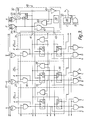
- apparatus for generating a signal representative of the position, within a sequence of binary digits (bits), of that bit or pair of bits of value "1" which lies at the centre of the or each largest group of bits of value "1" comprises a number N of substantially identical subcircuits 26, of which only three, 26 n-1 26 n and 26 n+1 , are shown in detail, and of which only one, 26 n , will be described in detail.
- N is equal to the number of bits in the entire sequence.
- the subcircuit 26 n has a data input 27 for the relevant bit of the sequence, which input feeds one input of a two-input AND gate 18.
- the output of AND gate 18 is connected to the J-input of a J-K flip-flop 19 the Q-output of which is connected to the D-input of a D-type flip-flop 20.
- the K -input of flip-flop 19 is fed from the output of an AND gate 28 the two inputs of which are fed from the Q-outputs of the J-K flip-flops corresponding to flip-flop 19 in the sub-circuits 26 n-1 and 26 n+1 corresponding to the immediately adjacent bits in the sequence.
- the Q-output of flip-flop 20 may, if desired, be connected to one input of each of two two-input NAND gates 21 and 25 respectively.
- NAND gates 21 and 25 are fed with the inverted and non-inverted values respectively of the signal appearing at the Q-output of the D-type flip-flop corresponding to flip-flop 20 in the subcircuit 26 n-1 corresponding to the immediately preceding bit in the sequence.
- the output of NAND-gate 21, denoted by the letter "C”, is, if present, connected to a corresponding input of an N-input priority encoder 48.
- NAND-gate 25 denoted by the letter "B”
- N-input AND-gate 29 the output of which, if present, supplies a least-significant bit to the (active low) multibit parallel output 30 from encoder 48 (if present).
- the other input of AND-gate 18 is fed from a control signal output 31 of a controllable clock pulse generator and control signal generator circuit 32.
- the output of AND-gate 18, denoted by the letter “A”, is also connected to a corresponding input of an N-input OR-gate 33, and the Q-output of J-K flip-flop 19, denoted by the letter “E” is also connected to a corresponding input of an N-input OR-gate 34.
- the outputs of the OR-gates 33 and 34 are connected to an input 35 and an inhibit signal input 36 respectively of generator circuit 32.
- the input 27 of sub-circuit 26 n may, if desired, be fed from an input terminal 37 of a three-input OR-gate 38 the other two inputs of which are fed from the inputs, corresponding to input 37, of similarly optional OR-gates corresponding to OR-gate 38 feeding the subcircuits 26 n-1 and 26 n+1 respectively.
- the "clear" inputs CLR of the flip-flops 19 and 20, and also of a flip-flop 44, are connected to a reset input 46.
- Generator circuit 32 comprises a clock pulse generator 39 which feeds one input of an AND-gate 40.
- the output of AND-gate 40 is connected to a clock signal output 41 of generator circuit 32 and also to an input of an AND-gate 42.
- the output of AND-gate 42 is connected to a clock signal output 43 of generator circuit 32.
- the output of pulse generator 32 is also connected to the clock input of the J-K flip-flop 44 the Q-output of which is connected to the second input of AND-gate 40.
- the inputs 35 and 36 of the generator circuit 32 are connected to the J-input of flip-flop 44 and to both the K -input of flip-flop 44 and the other input of AND-gate 42 respectively.
- the Q-output of flip-flop 44 is also connected to the output 31 of generator circuit 32 via an inverter 45.
- the outputs 41 and 43 of the generator circuit 32 are connected to the clock inputs of the J-K flip-flops 19 in all the subcircuits 26 and to the clock inputs of the D-type flip-flops 20 in all the subcircuits 26 respectively.
- the apparatus of Fig. 3 operates as follows, the inputs 27 of the various sub-circuits 26 being fed, for example, with binary digits from the outputs of respective comparators which compare the output signal amplitudes from respective feeds from a multi-beam antenna with a reference or threshold, as referred to in the preamble.
- OR-gate 33 The resulting binary "1" from OR-gate 33 allows flip-flop 44 to change state on the leading edge of the next clock pulse from generator 39, enabling AND-gate 40 and hence causing the input sequence present on the outputs of the AND-gates 18 to be written into first storage means comprising the flip-flops 19 (whose K -inputs are initially all logic "0") and disabling the AND-gates 18.
- the former operation gives rise to a logic "1" from OR-gate 34 and the latter operation gives rise to a logic "0" from OR-gate 33, causing flip-flop 44 to be held in the set state and AND-gate 42 to be enabled, the latter causing the input sequence to also be written into the flip-flops 20 (which form second storage means).
- flip-flop 44 is reset (its J and K inputs are now both logic "0") blocking AND-gate 40.
- the end result therefore, is that the flip-flops 20 in subcircuits 268 and 269 are in the set state, and all the other flip-flops 20 are in the reset state, indicating that the position of the pair of binary "1"s which lies at the centre of the largest group of binary "1"s in the sequence of Fig. 2 coincides with that of bits 8 and 9 in the sequence.
- the NAND gates 21 and 25, the priority encoder 48 (which may, for example, comprise several cascaded integrated circuits available under the type number 74148) and the AND-gate 29 (if present) are provided to transform this information into a more convenient form. It will be seen that the NAND gate 25 in a given sub-circuit 26 n produces a logic "0" if and only if the flip-flops 20 in both subcircuit 26 n and subcircuit 26 n-1 are both set, i.e. if the end result is a pair of flip-flops 20 being in the set state, rather than just one.
- the NAND gate 21 in a given subcircuit 26 n produces a logic "0" if and only if the flip-flops 20 in subcircuits 26 n and 26 n-1 are in the set and the reset state respectively.
- a logic "0” appears at the output C of that subcircuit of which the flip-flop 20 contains the left-most "1” in the sequence after the 1-stripping operations have been completed, and a logic "0" occurs at the output B of the immediately neighbouring subcircuit higher in the sequence if the flip-flop 20 in that subcircuit too contains a binary "1".
- the priority encoder 48 (which in the present example operates with inverted logic) responds to the outputs C by generating an output in inverted binary notation giving the number of that subcircuit which is generating the left-most "0", i.e. in the present example subcircuit 8, and AND gate 29 adds a least significant bit to this (in the present example binary "0" because of the inverted notation used) because output B of subcircuit 9 is producing a logic "0".
- the number in inverted binary notation on parallel output 30 is 8.5 as required.
- bit 12 in the original sequence had been binary "0”, meaning that the centre of the largest group of 1's was located actually at bit 8, rather than between bits 8 and 9, only the flip-flop 20 in subcircuit 268 would have been in the set state after the 1-stripping operations, resulting in all gates 25, and hence also gate 29, generating a logic 1, so that the number in inverted binary notation on output 30 would in that case have been 8.0 as required.
- bits applied to the inputs 27 are in fact derived from the outputs of respective comparators which compare the output signal amplitudes from respective feeds from a multi-beam antenna with a reference or threshold, it may be that one or more of these feeds or associated circuitry becomes faulty, with the result that the or each corresponding comparator produces a binary "0" rather than a binary "1". In, for example, a passive-direction-finding radio receiver this could lead to a quite erroneous result. For example, the sequence shown in Fig.
- the OR-gates 38 in Fig. 3 may be provided to at least reduce the magnitude of such an error, the comparator outputs being applied to the respective inputs 37 of these gates rather than direct to the subcircuit inputs 27.
- the arrangement employing J-K flip-flops is preferred because difficulties are liable to be encountered when the two-shift-register arrangement is used to process sequences in which two groups of logic "1"s are close together; when this is the case it may be that one group in one shift register starts to "overlap" the other group in the other shift register before it has ceased to overlap the one group in the other shift register.
- the array of flip-flops 20 of Fig. 3 will, if the largest group of "1"s in the initial sequence is accompanied by one or more other groups of the same size, produce output signals corresponding to each of these groups.
- the priority encoder 48 if present will only respond to one of these groups. The chance of this occurring can, if desired, be reduced by replacing the single gate 29/encoder 48 arrangement shown by a plurality of such arrangements each operating on signals derived from a different portion of the array of flip-flops 20 and collectively covering the whole array.
- the array of flip-flops 20 will produce an output signal corresponding to this other group in addition to one corresponding to the largest group.
- Fig. 4 shows how the embodiment of the invention shown in Fig. 3 may be incorporated in a passive direction-finding radio receiver.
- the apparatus of Fig. 3 is denoted by reference numeral 50 and the inputs 371 - 37 N thereof are supplied with data bits derived from respective feeds 511 - 51 N from a multi-beam antenna 52, for example of the Luneberg lens type, by means of respective amplitude detectors 531 - 53 N and respective comparators 541 - 54 N .
- at least an amplifier (which may be logarithmic) will be included in the coupling from each feed 51 to the corresponding comparator 5.
Landscapes
- Engineering & Computer Science (AREA)
- Physics & Mathematics (AREA)
- General Physics & Mathematics (AREA)
- Theoretical Computer Science (AREA)
- Radar, Positioning & Navigation (AREA)
- Remote Sensing (AREA)
- General Engineering & Computer Science (AREA)
- Variable-Direction Aerials And Aerial Arrays (AREA)
Applications Claiming Priority (1)
| Application Number | Priority Date | Filing Date | Title |
|---|---|---|---|
| GB08412475A GB2192764B (en) | 1984-05-16 | 1984-05-16 | Detecting the position, within a sequence of data elements of first and second kinds, of that element or pair of elements which lies at the centre of the or each largest group of elements of the first kind |
Publications (1)
| Publication Number | Publication Date |
|---|---|
| EP0322483A1 true EP0322483A1 (de) | 1989-07-05 |
Family
ID=10561035
Family Applications (1)
| Application Number | Title | Priority Date | Filing Date |
|---|---|---|---|
| EP87202504A Withdrawn EP0322483A1 (de) | 1984-05-16 | 1987-12-14 | Standortsanzeige eines Datenelementes |
Country Status (2)
| Country | Link |
|---|---|
| EP (1) | EP0322483A1 (de) |
| GB (1) | GB2192764B (de) |
Families Citing this family (3)
| Publication number | Priority date | Publication date | Assignee | Title |
|---|---|---|---|---|
| GB2192764B (en) * | 1984-05-16 | 1988-05-25 | Philips Electronic Associated | Detecting the position, within a sequence of data elements of first and second kinds, of that element or pair of elements which lies at the centre of the or each largest group of elements of the first kind |
| US4857937A (en) * | 1987-12-14 | 1989-08-15 | U.S. Philips Corporation | Data element position indication |
| GB2243041B (en) * | 1990-04-11 | 1994-02-23 | Philips Electronic Associated | Direction finding system |
Citations (4)
| Publication number | Priority date | Publication date | Assignee | Title |
|---|---|---|---|---|
| US3449711A (en) * | 1965-08-30 | 1969-06-10 | Magnavox Co | Beam former |
| DE1516876A1 (de) * | 1966-05-20 | 1969-07-24 | Telefunken Patent | Peiler |
| DE2925657A1 (de) * | 1979-06-26 | 1981-01-15 | Licentia Gmbh | Schaltungsanordnung zur ermittlung des tangenswerts eines peilwinkels aus den peilkomponenten |
| GB2192764A (en) * | 1984-05-16 | 1988-01-20 | Philips Electronic Associated | Detecting the position, within a sequence of data elements of first and second kinds, of that element or pair of elements which lies at the centre of the or each largest group of elements of the first kind |
-
1984
- 1984-05-16 GB GB08412475A patent/GB2192764B/en not_active Expired
-
1987
- 1987-12-14 EP EP87202504A patent/EP0322483A1/de not_active Withdrawn
Patent Citations (5)
| Publication number | Priority date | Publication date | Assignee | Title |
|---|---|---|---|---|
| US3449711A (en) * | 1965-08-30 | 1969-06-10 | Magnavox Co | Beam former |
| GB1173365A (en) * | 1965-08-30 | 1969-12-10 | Magnavox Co | Improvements in or relating to beam forming apparatus |
| DE1516876A1 (de) * | 1966-05-20 | 1969-07-24 | Telefunken Patent | Peiler |
| DE2925657A1 (de) * | 1979-06-26 | 1981-01-15 | Licentia Gmbh | Schaltungsanordnung zur ermittlung des tangenswerts eines peilwinkels aus den peilkomponenten |
| GB2192764A (en) * | 1984-05-16 | 1988-01-20 | Philips Electronic Associated | Detecting the position, within a sequence of data elements of first and second kinds, of that element or pair of elements which lies at the centre of the or each largest group of elements of the first kind |
Non-Patent Citations (2)
| Title |
|---|
| MILITARY MICROWAVES CONFERENCE PROCEEDINGS, 20-22nd October 1982, pages 512-518, Turnbridge Wells, Kent, GB; K.E. CASSEL: "A broad band ESM/ECM antenna with 360 degrees multibeam coverage" * |
| PROCEEDINGS OF THE IEEE, vol. 58, no. 12, December 1970, pages 1956-1957, IEEE, New York, US; C.M. COOK et al.: "Size detectors" * |
Also Published As
| Publication number | Publication date |
|---|---|
| GB2192764A (en) | 1988-01-20 |
| GB8412475D0 (en) | 1987-10-07 |
| GB2192764B (en) | 1988-05-25 |
Similar Documents
| Publication | Publication Date | Title |
|---|---|---|
| US4616330A (en) | Pipelined multiply-accumulate unit | |
| US5535402A (en) | System for (N•M)-bit correlation using N M-bit correlators | |
| US4524345A (en) | Serial comparison flag detector | |
| US4775952A (en) | Parallel processing system apparatus | |
| US3938087A (en) | High speed binary comparator | |
| US4857937A (en) | Data element position indication | |
| US4648059A (en) | N-bit magnitude comparator | |
| EP0322483A1 (de) | Standortsanzeige eines Datenelementes | |
| EP0265080B1 (de) | Einrichtung zur Ermittlung der Bit-Phasendifferenz | |
| WO1981000472A1 (en) | Incrementer/decrementer circuit | |
| Bass et al. | On finding the disc of minimum radius containing a given set of points | |
| US3213453A (en) | Digital direction finder utilizing binary array | |
| US11861325B2 (en) | Repurposed hexadecimal floating point data path | |
| US3622985A (en) | Optimum error-correcting code device for parallel-serial transmissions in shortened cyclic codes | |
| US6839861B2 (en) | Method and system for selecting data sampling phase for self timed interface logic | |
| CA1109157A (en) | Word recognizing system | |
| US4879675A (en) | Parity generator circuit and method | |
| US4860241A (en) | Method and apparatus for cellular division | |
| US4896323A (en) | Parity-checked clock generator system | |
| EP0363475B1 (de) | Verfahren zur objektzuordnung | |
| EP1383050A1 (de) | Verfahren und Gerät zur Erkennung doppelter Eintragungen in einer Nachschlagtabelle | |
| US3439328A (en) | Parity circuits employing threshold gates | |
| US4084253A (en) | Current mode arithmetic logic circuit with parity prediction and checking | |
| US7027649B1 (en) | Computing the Euler number of a binary image | |
| US4355312A (en) | Radar signal processor |
Legal Events
| Date | Code | Title | Description |
|---|---|---|---|
| PUAI | Public reference made under article 153(3) epc to a published international application that has entered the european phase |
Free format text: ORIGINAL CODE: 0009012 |
|
| AK | Designated contracting states |
Kind code of ref document: A1 Designated state(s): DE IT SE |
|
| 17P | Request for examination filed |
Effective date: 19891220 |
|
| 17Q | First examination report despatched |
Effective date: 19920507 |
|
| STAA | Information on the status of an ep patent application or granted ep patent |
Free format text: STATUS: THE APPLICATION IS DEEMED TO BE WITHDRAWN |
|
| 18D | Application deemed to be withdrawn |
Effective date: 19920918 |
|
| RIN1 | Information on inventor provided before grant (corrected) |
Inventor name: DADDS, ALAN FREDERICK |