EP0321801A1 - Turn-off thyristor with overvoltage protection - Google Patents
Turn-off thyristor with overvoltage protection Download PDFInfo
- Publication number
- EP0321801A1 EP0321801A1 EP88120593A EP88120593A EP0321801A1 EP 0321801 A1 EP0321801 A1 EP 0321801A1 EP 88120593 A EP88120593 A EP 88120593A EP 88120593 A EP88120593 A EP 88120593A EP 0321801 A1 EP0321801 A1 EP 0321801A1
- Authority
- EP
- European Patent Office
- Prior art keywords
- zone
- fet
- anode
- gate
- cathode
- Prior art date
- Legal status (The legal status is an assumption and is not a legal conclusion. Google has not performed a legal analysis and makes no representation as to the accuracy of the status listed.)
- Granted
Links
- 230000004224 protection Effects 0.000 title claims abstract description 21
- 239000000758 substrate Substances 0.000 claims description 15
- 238000001465 metallisation Methods 0.000 claims description 3
- 238000000926 separation method Methods 0.000 abstract description 2
- 239000003990 capacitor Substances 0.000 description 4
- 238000001816 cooling Methods 0.000 description 4
- 238000006073 displacement reaction Methods 0.000 description 3
- 230000003321 amplification Effects 0.000 description 2
- 238000001514 detection method Methods 0.000 description 2
- 230000010354 integration Effects 0.000 description 2
- 238000003199 nucleic acid amplification method Methods 0.000 description 2
- 230000015572 biosynthetic process Effects 0.000 description 1
- 230000015556 catabolic process Effects 0.000 description 1
- 239000000919 ceramic Substances 0.000 description 1
- 238000009795 derivation Methods 0.000 description 1
- 238000005538 encapsulation Methods 0.000 description 1
- 230000005669 field effect Effects 0.000 description 1
- 238000004519 manufacturing process Methods 0.000 description 1
- 230000009979 protective mechanism Effects 0.000 description 1
- 239000004065 semiconductor Substances 0.000 description 1
- 230000035945 sensitivity Effects 0.000 description 1
- 229910052710 silicon Inorganic materials 0.000 description 1
- 239000010703 silicon Substances 0.000 description 1
- 238000009827 uniform distribution Methods 0.000 description 1
Images

Classifications
-
- H—ELECTRICITY
- H03—ELECTRONIC CIRCUITRY
- H03K—PULSE TECHNIQUE
- H03K17/00—Electronic switching or gating, i.e. not by contact-making and –breaking
- H03K17/08—Modifications for protecting switching circuit against overcurrent or overvoltage
- H03K17/082—Modifications for protecting switching circuit against overcurrent or overvoltage by feedback from the output to the control circuit
- H03K17/0824—Modifications for protecting switching circuit against overcurrent or overvoltage by feedback from the output to the control circuit in thyristor switches
Definitions
- the present invention relates to the field of power semiconductors. It relates in particular to a thyristor that can be switched off with overvoltage protection, in particular for use in a series connection of several thyristors, which thyristor that can be switched off has an anode, a cathode and a gate.
- the thyristors are therefore connected in series. This is possible because you can master the necessary uniform distribution of the total voltage between the individual elements by simultaneous ignition and a suitable additional circuit.
- Such an additional circuit for conventional thyristors is known, for example, from SCR Manual, 5th Edition (1972) from General Electric, pp. 156-159. On the one hand, it can be designed as a so-called “snubber” circuit composed of passive elements such as resistors and capacitors (FIG. 6.7 there).
- it can also include active elements such as varistors or avalanche diodes (Fig. 6.9), which become conductive above a critical voltage and thus represent active overvoltage protection.
- active elements such as varistors or avalanche diodes (Fig. 6.9), which become conductive above a critical voltage and thus represent active overvoltage protection.
- EP-A2 0209 986 it is also known (EP-A2 0209 986) to provide an avalanche zone in the case of a conventional thyristor with an “amplifying gate” as overvoltage protection within the substrate, said zone being controlled at a critical voltage and switching on the thyristor part via its gate.
- the disadvantage here is that the thyristor itself is used to reduce the overvoltage, so there is no protective mechanism independent of the thyristor.
- GTOs and FCThs are said to operate at a relatively high frequency. Because of the storage time specific to these thyristors, their switch-off time depends heavily on the control. At the same time, the size of the storage charge differs at least as much for the individual elements as for conventional thyristors. The consequence of this is that a corresponding snubber circuit would have to be very powerful, which would lead to a disproportionately high power loss.
- thyristors that can be switched off only have active overvoltage protection in the form of an arrester (varistor or avalanche diode) in question.
- an arrester variant or avalanche diode
- such arresters must be designed for quite high outputs: at 4 kV clamping voltage, 1000 A switch-off current, 2 kHz repetition frequency and 0.3 microsecond loading of the arrester per period, there is a power loss of 2.4 kW per arrester .
- ZnO varistors too, cannot dissipate much more than 200 W of power due to their low thermal conductivity (the ceramic), the encapsulation and cooling of such elements being about as complex as that of high-performance thyristors.
- the object of the present invention is to provide a thyristor that can be switched off and has overvoltage protection, which requires comparatively little additional effort and can be implemented using known means.
- the problem is solved in a thyristor of the type mentioned above that -
- the overvoltage protection comprises a controllable resistor and an overvoltage sensor;
- the controllable resistor is connected to the turn-off thyristor in parallel between its anode and its cathode, and - Is controlled by the overvoltage sensor.
- the essence of the invention is therefore not to use a single heavy-duty component for overvoltage detection and voltage limitation, but to carry out the overvoltage detection with an overvoltage sensor of lower load capacity and to control a more resilient, controllable resistance with this sensor, which can be optimally adapted to the requirements.
- the thyristor that can be switched off is an FCTh
- the controllable resistor is a J-FET
- both are integrated next to one another on a common substrate.
- the overvoltage sensor can be a varistor or an avalanche diode, which can also be integrated into the substrate.
- the invention takes a completely different route: the switchable thyristor AT is connected in parallel between its anode A1 and its cathode K1 (FIG. 2), which is operated by an overvoltage sensor OS is controlled.
- the overvoltage sensor OS detects the overvoltage condition on the thyristor AT which can be switched off and then controls the controllable resistor in such a way that the overvoltage is reduced via it.
- controllable resistor is a J-FET (JF), the source S of which is connected to the cathode K1 and the drain D of which is connected to the anode A1 of the turn-off thyristor AT.
- JF J-FET
- controllable resistance can be optimally designed for the dissipated power dissipation.
- the controllable resistor in the form of a J-FET can be integrated directly with the thyristor on a common substrate, the same manufacturing technology and geometry being able to be used for both components (FIG. 4).
- Such an integrated avalanche zone would have to have an area larger than 5 cm2 in order to be able to dissipate the power loss in the range of several kW.
- a large area requires an unattainable homogeneity of the electrical properties in the avalanche zone, so that not only a few points in the zone take over the entire leakage current.
- FIG. 3A A first exemplary embodiment of a complete thyristor stage with drive circuit and overvoltage protection according to the invention is shown in FIG. 3A.
- a cascade circuit comprising the switchable thyristor AT and an auxiliary thyristor HT is provided on the control side. Both thyristors are FCThs.
- the drive circuit further comprises a capacitor C, a series resistor RV1 and a voltage source VS.
- a gate voltage V G1 is present at the capacitor C; the auxiliary thyristor is driven by an input signal V IN .
- FCThs are thyristors that are conductive in the event of a short circuit between the gate and cathode (so-called "normally-ON" components)
- the voltage source VS is eliminated;
- the series resistor RV1 is then directly on the cathode K1.
- the voltage source VS has a voltage of approximately 5 V.
- the overvoltage protection of the thyristor stage comprises the parallel-connected J-FET JF, a varistor V (or an avalanche diode AD) as an overvoltage sensor, and a gate resistor RG.
- the varistor V is connected between the gate G2 and the drain D of the J-FET and has e.g. a kink voltage of 4 kV.
- the gate resistor RG connects the gate G2 to the gate G1 of the turn-off thyristor AT. This has the special advantage that simple integration of the overvoltage protection is possible.
- the varistor V in the circuit according to FIG. 3A still carries a relatively high part of the total power loss and must therefore be chosen to be correspondingly large.
- an additional amplification stage is therefore provided between the varistor V and the J-FET in a second exemplary embodiment (FIG. 3B), which in the example comprises a transistor T and a second series resistor RV2.
- the varistor V can be designed at least 10 times smaller.
- the transistor T is otherwise supplied by the same voltage source VS as the thyristor cascade HT, AT.
- FCTh as the thyristor AT which can be switched off and to integrate it with the J-FET on a common substrate according to FIG. 4 (possibly together with an avalanche zone as an overvoltage sensor).
- the 2.4 kW average power assumed at the beginning would mean a power loss of 500 W / cm2, which is also at the upper limit even with very good cooling. Since a corresponding GTO thyristor or FCTh requires an area of at least 20 cm2 anyway, the area of the J-FET can be increased somewhat without difficulty.
- a varistor e.g. the series connection of two varistors of the type SIOV-S14K680 and SIOV-S14K1000 from Siemens in question.
- the voltage at 1A is then about 4 kV, the capacitance 80 pF.
- the varistors at a repetition frequency of 2 kHz and a load of 0.3 microseconds per period result in a power loss of 9.6 W, which can be easily dissipated by direct cooling.
- FCTh and J-FET (and in addition an avalanche zone or diode) will now be explained using the exemplary embodiment in FIG. 4, in which a corresponding substrate is shown in sections in cross section.
- the substrate is laterally divided into three areas.
- the FCTh structure is arranged in the left area, the J-FET structure in the middle area, and the avalanche diode structure (AD) in the right area.
- AD avalanche diode structure
- the FCTh structure is of the "recessed gate” type with a step-shaped gate-cathode structure which has a plurality of control fingers 9 separated by trenches.
- Such an FCTh is e.g. known from EP-A2 0 178 387.
- the FCTh structure comprises between the anode A1 and the cathode K1 a layer sequence of a p+-doped anode zone 7, an n ⁇ -doped channel layer 5, a p-doped gate zone 4 and n+-doped cathode regions 2.
- the cathode regions 2 are arranged on the top of the control fingers 9.
- the channel layer 5 extends into this control finger 9 and borders there on the cathode regions 2.
- the gate zone 4 extends in each case over the bottoms and walls of the trenches and, together with the channel layer 5 running in the control finger, forms a long channel which can be controlled by a field effect.
- the gate zone 4 is provided on the trench floors with gate contacts 3, the cathode regions 2 on the control fingers 9 with corresponding cathode contacts 1.
- a large-area anode contact 8 establishes the electrical connection to the anode zone 7.
- the structure and geometry of the J-FET structure in the central region of the substrate is comparable to that of the neighboring FCTh structure, with the difference that here a n-doped drain zone 15 takes the place of the p-doped anode zone 7.
- n-doped buffer layer 6 which runs below the channel layers 5, 14 and separates the anode zone 7 and drain zone 15 from one another and from these channel layers.
- the drain D of the J-FET is connected to the anode A1 of the FCTh.
- the cathode contacts 1 and the source contacts 10 can be brought together to form a common connection.
- the J-FET then lies with its source S on the cathode K1 of the FCTh.
- the gate G2 of the J-FET lies above the gate resistor RG at the gate G1 of the FCTh.
- This gate resistance RG is expediently realized in that the gate contacts 3 and 12 of the FCTh or J-FET, which are on the same level, are not designed as a continuous metallization layer, but instead have a gap between them with a correspondingly selected distance d. The part of the gate zone 4, 13 below this gap then forms the desired gate resistance RG.
- an avalanche diode AD is provided as an overvoltage sensor instead of an external varistor V, this diode can also be integrated into the substrate in the form of an avalanche zone, as shown in FIG. 4 (right area).
- the diode structure comprises a sequence of four zones 18, 19, 20 and 21.
- the first zone 18 is p+-doped and a continuation of the gate zone 13 of the adjacent J-FET.
- the second zone 19 is n ⁇ -doped and a continuation of the channel layer 14, but with a reduced thickness in order to achieve suitable breakdown voltages.
- the third zone 20 is n-doped and a direct continuation of the buffer layer 6.
- the fourth zone 21 is n+-doped and is a direct continuation of the drain zone 15.
- Both the anode contact 17 and the cathode contact 22 are respectively continuations of the gate contact 12 and the drain contact 16.
- FCTh FCTh
- J-FET J-FET
- AD AD
- the disconnectable thyristor according to the invention provides a component that is protected against overvoltages and that can be implemented with little effort, compactly constructed and easily integrated.
Landscapes
- Thyristors (AREA)
- Junction Field-Effect Transistors (AREA)
Abstract
Bei einem abschaltbaren Thyristor (AT) mit Ueberspannungsschutz wird die Spannungsbegrenzung durch einen parallelgeschalteten steuerbaren Widerstand, insbesondere in Form eines J-FET (JF) erreicht, der durch einen Ueberspannungssensor (OS) angesteuert wird. Durch die Trennung von Sensor- und Ableitfunktion ergeben sich Vorteile für einen einfachen und kompakten Aufbau.In the case of a thyristor (AT) which can be switched off and has overvoltage protection, the voltage limitation is achieved by means of a controllable resistor connected in parallel, in particular in the form of a J-FET (JF) which is controlled by an overvoltage sensor (OS). The separation of sensor and drainage functions results in advantages for a simple and compact structure.
Description
Die vorliegende Erfindung bezieht sich auf das Gebiet der Leistungshalbleiter. Sie betrifft speziell einen abschaltbaren Thyristor mit Ueberspannungsschutz, insbesondere für den Einsatz in einer Serieschaltung mehrerer Thyristoren, welcher abschaltbare Thyristor eine Anode, eine Kathode und ein Gate aufweist.The present invention relates to the field of power semiconductors. It relates in particular to a thyristor that can be switched off with overvoltage protection, in particular for use in a series connection of several thyristors, which thyristor that can be switched off has an anode, a cathode and a gate.
Während bei den verhältnismässig kleinen Strömen, die mit IGTs (Insulated Gate Transistors) und Leistungs-MOSFETs geschaltet werden, Betriebsspannungen über 1000 V selten sind, arbeiten herkömmliche Thyristoren und abschaltbare Thyristoren (z.B. GTO-Thyristoren) oft in Netzen mit weit höherer Spannung (einige 10 bis einige 100 kV).While in the comparatively small streams that are connected with IGT (Insulated Gate T ransistors) and power MOSFETs operating voltages greater than 1000 V are rare, conventional thyristors and turn-off thyristors (eg GTOs) often operate in networks with much higher Voltage (some 10 to some 100 kV).
Die Thyristoren werden deshalb in Serie geschaltet. Dies ist möglich, weil man die notwendige gleichmässige Aufteilung der Gesamtspannung auf die einzelnen Elemente durch gleichzeitiges Zünden und eine geeignete Zusatzbeschaltung beherrschen kann.The thyristors are therefore connected in series. This is possible because you can master the necessary uniform distribution of the total voltage between the individual elements by simultaneous ignition and a suitable additional circuit.
Eine derartige Zusatzbeschaltung für herkömmliche Thyristoren ist beispielsweise aus dem SCR Manual, 5th Edition (1972) von der Firma General Electric, S. 156 - 159, bekannt. Sie kann einerseits als sogenannte "Snubber"-Beschaltung aus passiven Elementen wie Widerständen und Kondensatoren ausgeführt sein (dortige Fig. 6.7).Such an additional circuit for conventional thyristors is known, for example, from SCR Manual, 5th Edition (1972) from General Electric, pp. 156-159. On the one hand, it can be designed as a so-called “snubber” circuit composed of passive elements such as resistors and capacitors (FIG. 6.7 there).
Sie kann andererseits aber auch aktive Elemente wie Varistoren oder Avalanchedioden umfassen (Fig. 6.9), die oberhalb einer kritischen Spannung leitend werden und damit einen aktiven Ueberspannungsschutz darstellen.On the other hand, it can also include active elements such as varistors or avalanche diodes (Fig. 6.9), which become conductive above a critical voltage and thus represent active overvoltage protection.
Weiterhin ist es auch bekannt (EP-A2 0209 986) bei einem herkömmlichen Thyristor mit "amplifying gate" innerhalb des Substrats als Ueberspannungsschutz eine Avalanchezone vorzusehen, die bei einer kritischen Spannung durchsteuert und den Thyristorteil über sein Gate einschaltet. Nachteilig ist hier jedoch, dass der Thyristor selbst zum Ueberspannungsabbau verwendet wird, also kein vom Thyristor unabhängiger Schutzmechanismus existiert.Furthermore, it is also known (EP-A2 0209 986) to provide an avalanche zone in the case of a conventional thyristor with an “amplifying gate” as overvoltage protection within the substrate, said zone being controlled at a critical voltage and switching on the thyristor part via its gate. The disadvantage here, however, is that the thyristor itself is used to reduce the overvoltage, so there is no protective mechanism independent of the thyristor.
Während sich bei den herkömmlichen, nicht abschaltbaren Thyristoren der beschriebene Ueberspannungsschutz bewährt hat, treten bei abschaltbaren Thyristoren (GTO-Thyristoren und FCThs = Field Controlled Thyristors) neue Probleme auf.During the overvoltage protection described has proven itself in the conventional non thyristors, new problems occur during turn-off thyristors (GTOs and FCThs = F ield C ontrolled Th yristors).
GTOs und FCThs sollen mit verhältnismässig hoher Frequenz arbeiten. Ihr Ausschaltzeitpunkt hängt wegen der für diese Thyristoren spezifischen Speicherzeit stark von der Ansteuerung ab. Gleichzeitig streut die Grösse der Speicherladung bei den einzelnen Elementen mindestens genauso stark wie bei herkömmlichen Thyristoren. Das hat zur Folge, dass eine entsprechende Snubber-Beschaltung leistungsmässig sehr stark ausgelegt werden müsste, was zu einer unverhältnismässig grossen Verlustleistung führen würde.GTOs and FCThs are said to operate at a relatively high frequency. Because of the storage time specific to these thyristors, their switch-off time depends heavily on the control. At the same time, the size of the storage charge differs at least as much for the individual elements as for conventional thyristors. The consequence of this is that a corresponding snubber circuit would have to be very powerful, which would lead to a disproportionately high power loss.
Aus diesem Grunde kommt bei abschaltbaren Thyristoren nur ein aktiver Ueberspannungsschutz in Form eines Ableiters (Varistor oder Avalanchediode) in Frage. Trotz der kurzen Schaltzeiten speziell von FCThs müssen solche Ableiter für recht hohe Leistungen ausgelegt sein: Bei 4 kV Klemmspannung, 1000 A Abschaltstrom, 2 kHz Wiederholfrequenz und 0,3 Mikrosekunden Belastung des Ableiters pro Periode ergibt sich eine Verlustleistung von 2,4 kW pro Ableiter.For this reason, thyristors that can be switched off only have active overvoltage protection in the form of an arrester (varistor or avalanche diode) in question. Despite the short switching times, especially from FCThs, such arresters must be designed for quite high outputs: at 4 kV clamping voltage, 1000 A switch-off current, 2 kHz repetition frequency and 0.3 microsecond loading of the arrester per period, there is a power loss of 2.4 kW per arrester .
Avalanchedioden für solche Belastungen sind aber nicht bekannt. Auch ZnO-Varistoren können wegen ihrer geringen Wärmeleitfähigkeit (der Keramik) nicht weit über 200 W Leistung abführen, wobei die Kapselung und Kühlung solcher Elemente etwa gleich aufwendig ist, wie diejenige von Hochleistungsthyristoren.Avalanche diodes for such loads are not known. ZnO varistors, too, cannot dissipate much more than 200 W of power due to their low thermal conductivity (the ceramic), the encapsulation and cooling of such elements being about as complex as that of high-performance thyristors.
Aufgabe der vorliegenden Erfindung ist es nun, einen abschaltbaren Thyristor mit Ueberspannungsschutz zu schaffen, der vergleichsweise wenig zusätzlichen Aufwand erfordert und mit bekannten Mitteln realisiert werden kann.The object of the present invention is to provide a thyristor that can be switched off and has overvoltage protection, which requires comparatively little additional effort and can be implemented using known means.
Die Aufgabe wird bei einem abschaltbaren Thyristor der eingangs genannten Art dadurch gelöst, dass
- der Ueberspannungsschutz einen steuerbaren Widerstand und einen Ueberspannungssensor umfasst;
- der steuerbare Widerstand dem abschaltbaren Thyristor zwischen seiner Anode und seiner Kathode parallel geschaltet ist, und
- von dem Ueberspannungssensor angesteuert wird.The problem is solved in a thyristor of the type mentioned above that
- The overvoltage protection comprises a controllable resistor and an overvoltage sensor;
- The controllable resistor is connected to the turn-off thyristor in parallel between its anode and its cathode, and
- Is controlled by the overvoltage sensor.
Der Kern der Erfindung besteht also darin, für Ueberspannungsdetektion und Spannungsbegrenzung nicht ein einziges hochbelastbares Bauelement einzusetzen, sondern die Ueberspannungsdetektion mit einem Ueberspannungssensor geringerer Belastbarkeit durchzuführen und mit diesem Sensor einen höher belastbaren regelbaren Widerstand anzusteuern, der den Erfordernissen optimal angepasst werden kann.The essence of the invention is therefore not to use a single heavy-duty component for overvoltage detection and voltage limitation, but to carry out the overvoltage detection with an overvoltage sensor of lower load capacity and to control a more resilient, controllable resistance with this sensor, which can be optimally adapted to the requirements.
Gemäss einem besonders bevorzugten Ausführungsbeispiel der Erfindung ist der abschaltbare Thyristor ein FCTh, der steuerbare Widerstand ein J-FET, und beide sind auf einem gemeinsamen Substrat nebeneinander integriert.According to a particularly preferred embodiment of the invention, the thyristor that can be switched off is an FCTh, the controllable resistor is a J-FET, and both are integrated next to one another on a common substrate.
Hierdurch wird ein äusserst kompaktes Bauelement realisiert, das bezüglich Gehäuse und Kühlung für den Ueberspannungsschutz keinen zusätzlichen Aufwand erfordert.In this way, an extremely compact component is realized, which requires no additional effort with regard to housing and cooling for the overvoltage protection.
Der Ueberspannungssensor kann hierbei ein Varistor sein, oder eine Avalanchediode, die auch noch in das Substrat integriert werden kann.The overvoltage sensor can be a varistor or an avalanche diode, which can also be integrated into the substrate.
Weitere Ausführungsbeispiele ergeben sich aus den Unteransprüchen.Further exemplary embodiments result from the subclaims.
Die Erfindung soll nachfolgend anhand von Ausführungsbeispielen im Zusammenhang mit der Zeichnung näher erläutert werden. Es zeigen:
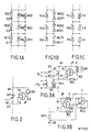
- Fig. 1A-C verschiedene Möglichkeiten der passiven und aktiven Ueberspannungsbegrenzung bei herkömmlichen Thyristoren nach dem Stand der Technik;
- Fig. 2 die Prinzipschaltung eines J-FET-Ueberspannungsschutzes für einen abschaltbaren Thyristor gemäss einem bevorzugten Ausführungsbeispiel der Erfindung;
- Fig. 3A eine vollständige Thyristorstufe mit Thyristorkaskade und Ueberspannungsschutz nach der Erfindung;
- Fig. 3B eine Fig. 3A entsprechende Thyristorstufe mit zusätzlicher Verstärkung zwischen dem Ueberspannungssensor und dem regelbaren Widerstand; und
- Fig. 4 das Ausführungsbeispiel eines FCTh mit integriertem J-FET und integrierter Avalanchediode.
- 1A-C different possibilities of passive and active overvoltage limitation in conventional thyristors according to the prior art;
- 2 shows the basic circuit of a J-FET overvoltage protection for a thyristor which can be switched off in accordance with a preferred exemplary embodiment of the invention;
- 3A shows a complete thyristor stage with a thyristor cascade and overvoltage protection according to the invention;
- 3B shows a thyristor stage corresponding to FIG. 3A with additional amplification between the overvoltage sensor and the controllable resistor; and
- Fig. 4 shows the embodiment of an FCTh with an integrated J-FET and an integrated avalanche diode.
In den Fig. 1A-C sind verschiedene Arten des Ueberspannungsschutzes für herkömmliche Thyristoren in Serieschaltung dargestellt, wie sie aus dem Stand der Technik bekannt sind.
- Fig. 1A zeigt speziell eine passive Snubber-Beschaltung, bei der jedem der Thyristoren Th1, ..., Th3 Kombinationen aus Widerständen R11, ..., R32 und Kondensatoren C1, ..., C3 parallelgeschaltet sind.
- Fig. 1B zeigt eine erste Variante eines aktiven Ueberspannungsschutzes, bei der jedem der Thyristoren Th1, ..., Th3 ein Paar von entgegengesetzt angeordneten Avalanchedioden AD11, 12 bzw. AD21, 22 bzw. AD31, 32 parallelgeschaltet ist.
- Fig. 1C schliesslich zeigt eine zweite Variante eines aktiven Ueberspannungsschutzes, bei dem anstelle der Avalanchedioden AD11, ..., AD32 Varistoren V1, ..., V3 vorgesehen sind.
- 1A specifically shows a passive snubber circuit in which each of the thyristors Th1, ..., Th3 combinations of resistors R11, ..., R32 and capacitors C1, ..., C3 are connected in parallel.
- 1B shows a first variant of an active overvoltage protection in which each of the thyristors Th1,..., Th3 has a pair of oppositely arranged avalanche diodes AD11, 12 or AD21, 22 or AD31, 32 connected in parallel.
- 1C finally shows a second variant of an active overvoltage protection, in which varistors V1, ..., V3 are provided instead of the avalanche diodes AD11, ..., AD32.
Wie bereits eingangs erwähnt, können diese bekannten Ueberspannungsschutz-Beschaltungen bei herkömmlichen Thyristoren ohne Probleme realisiert werden, weil dort wegen der relatiy geringen Schaltfrequenzen sehr viel weniger Verlustleistung anfällt.As already mentioned at the beginning, these known overvoltage protection circuits can be implemented without problems in conventional thyristors, because there is much less power dissipation due to the relatively low switching frequencies.
Bei abschaltbaren Thyristoren (GTO-Thyristoren und FCThs) mit ihren höheren Betriebsfrequenzen geht die Erfindung einen vollkommen anderen Weg: Dem abschaltbaren Thyristor AT wird zwischen seiner Anode A1 und seiner Kathode K1 ein steuerbarer Widerstand parallelgeschaltet (Fig. 2), der von einem Ueberspannungssensor OS angesteuert wird.In the case of switchable thyristors (GTO thyristors and FCThs) with their higher operating frequencies, the invention takes a completely different route: the switchable thyristor AT is connected in parallel between its anode A1 and its cathode K1 (FIG. 2), which is operated by an overvoltage sensor OS is controlled.
Der Ueberspannungssensor OS detektiert den Ueberspannungszustand am abschaltbaren Thyristor AT und steuert dann den steuerbaren Widerstand so, dass die Ueberspannung über ihn abgebaut wird.The overvoltage sensor OS detects the overvoltage condition on the thyristor AT which can be switched off and then controls the controllable resistor in such a way that the overvoltage is reduced via it.
Im Ausführungsbeispiel der Fig. 2 ist der steuerbare Widerstand ein J-FET (JF), dessen Source S mit der Kathode K1 und dessen Drain D mit der Anode A1 des abschaltbaren Thyristors AT verbunden ist.In the exemplary embodiment in FIG. 2, the controllable resistor is a J-FET (JF), the source S of which is connected to the cathode K1 and the drain D of which is connected to the anode A1 of the turn-off thyristor AT.
Da hier, anders als bei den Avalanchedioden und Varistoren aus Fig. 1B, C, Sensorfunktion und Ableitfunktion von getrennten Schaltungsteilen wahrgenommen werden, kann der steuerbare Widerstand optimal für die abzuführende Verlustleistung ausgelegt werden.Since here, unlike the avalanche diodes and varistors from FIGS. 1B, C, the sensor function and derivative function are performed by separate circuit parts, the controllable resistance can be optimally designed for the dissipated power dissipation.
Insbesondere wenn der abschaltbare Thyristor AT ein FCTh ist, kann der steuerbare Widerstand in Form eines J-FET direkt mit dem Thyristor auf einem gemeinsamen Substrat integriert werden, wobei für beide Bauelemente dieselbe Herstellungstechnologie und Geometrie verwendet werden kann (Fig. 4).Particularly if the thyristor AT that can be switched off is an FCTh, the controllable resistor in the form of a J-FET can be integrated directly with the thyristor on a common substrate, the same manufacturing technology and geometry being able to be used for both components (FIG. 4).
In diesem Zusammenhang kann deutlich gemacht werden, warum die erfindungsgemässe Trennung von Sensor- und Ableitfunktion vorteilhaft ist: Prinzipiell könnte in Analogie zu Fig. 1B in das Thyristorsubstrat auch eine Avalanchezone integriert werden, die beide Funktionen in sich vereint.In this context, it can be made clear why the separation of sensor and derivation function according to the invention is advantageous: In principle, analogous to FIG. 1B, an avalanche zone could also be integrated into the thyristor substrate, which combines both functions.
Eine solche integrierte Avalanchezone müsste, um die Verlustleistung im Bereich mehrerer kW abführen zu können, eine Fläche grösser 5 cm² aufweisen. Eine derart grosse Fläche erfordert aber eine nicht erreichbare Homogenität der elektrischen Eigenschaften in der Avalanchezone, damit nicht nur wenige Stellen der Zone den gesamten Ableitstrom übernehmen.Such an integrated avalanche zone would have to have an area larger than 5 cm² in order to be able to dissipate the power loss in the range of several kW. However, such a large area requires an unattainable homogeneity of the electrical properties in the avalanche zone, so that not only a few points in the zone take over the entire leakage current.
Ein erstes Ausführungsbeispiel für eine vollständige Thyristorstufe mit Ansteuerschaltung und Ueberspannungsschutz gemäss der Erfindung ist in Fig. 3A wiedergegeben.A first exemplary embodiment of a complete thyristor stage with drive circuit and overvoltage protection according to the invention is shown in FIG. 3A.
Auf der Ansteuerungsseite ist in dieser Stufe eine Kaskadenschaltung aus dem abschaltbaren Thyristor AT und einem Hilfsthyristor HT vorgesehen. Beide Thyristoren sind FCThs.In this stage, a cascade circuit comprising the switchable thyristor AT and an auxiliary thyristor HT is provided on the control side. Both thyristors are FCThs.
Die Ansteuerschaltung umfasst weiterhin einen Kondensator C, einen Vorwiderstand RV1 und eine Spannungsquelle VS. Am Kondensator C liegt eine Gatespannung VG1 an; der Hilfsthyristor wird durch ein Eingangssignal VIN angesteuert.The drive circuit further comprises a capacitor C, a series resistor RV1 and a voltage source VS. A gate voltage V G1 is present at the capacitor C; the auxiliary thyristor is driven by an input signal V IN .
Wenn es sich bei den FCThs um Thyristoren handelt, die bei Kurzschluss zwischen Gate und Kathode leitend sind (sog. "normally-ON"-Bauelemente), fällt die Spannungsquelle VS weg; der Vorwiderstand RV1 liegt dann direkt an der Kathode K1.If the FCThs are thyristors that are conductive in the event of a short circuit between the gate and cathode (so-called "normally-ON" components), the voltage source VS is eliminated; The series resistor RV1 is then directly on the cathode K1.
Sind die FCThs dagegen vom "normally-OFF"-Typ, hat die Spannungsquelle VS eine Spannung von etwa 5 V.In contrast, if the FCThs are of the "normally-OFF" type, the voltage source VS has a voltage of approximately 5 V.
Einzelheiten über die Funktionsweise einer solchen Thyristorkaskade können der EP-A2 0 246 478 entnommen werden.Details of the functioning of such a thyristor cascade can be found in EP-A2 0 246 478.
Der Ueberspannungsschutz der Thyristorstufe umfasst den parallelgeschalteten J-FET JF, einen Varistor V (oder eine Avalanchediode AD) als Ueberspannungssensor, und einen Gatewiderstand RG.The overvoltage protection of the thyristor stage comprises the parallel-connected J-FET JF, a varistor V (or an avalanche diode AD) as an overvoltage sensor, and a gate resistor RG.
Der Varistor V ist zwischen das Gate G2 und den Drain D des J-FET geschaltet und hat z.B. eine Knickspannung von 4 kV. Der Gatewiderstand RG verbindet das Gate G2 mit dem Gate G1 des abschaltbaren Thyristors AT. Dies hat den speziellen Vorteil, dass eine einfache Integration des Ueberspannungsschutzes möglich ist.The varistor V is connected between the gate G2 and the drain D of the J-FET and has e.g. a kink voltage of 4 kV. The gate resistor RG connects the gate G2 to the gate G1 of the turn-off thyristor AT. This has the special advantage that simple integration of the overvoltage protection is possible.
Der Varistor V in der Schaltung gemäss Fig. 3A trägt trotz des steuerbaren Widerstands immer noch einen relatiy hohen Teil der gesamten Verlustleistung und muss daher entsprechend gross gewählt werden.In spite of the controllable resistance, the varistor V in the circuit according to FIG. 3A still carries a relatively high part of the total power loss and must therefore be chosen to be correspondingly large.
Um einen kleineren Varistor einsetzen zu können, ist daher in einem zweiten Ausführungsbeispiel (Fig. 3B) zwischen dem Varistor V und dem J-FET eine zusätzliche Verstärkungsstufe vorgesehen, die im Beispiel einen Transistor T und einen zweiten Vorwiderstand RV2 umfasst. Mit einer solchen zusätzlichenIn order to be able to use a smaller varistor, an additional amplification stage is therefore provided between the varistor V and the J-FET in a second exemplary embodiment (FIG. 3B), which in the example comprises a transistor T and a second series resistor RV2. With such an additional
Verstärkungsstufe kann der Varistor V wenigstens 10 mal kleiner ausgelegt sein. Der Transistor T wird bei dieser Schaltung im übrigen durch dieselbe Spannungsquelle VS versorgt, wie die Thyristorkaskade HT, AT.Gain stage, the varistor V can be designed at least 10 times smaller. In this circuit, the transistor T is otherwise supplied by the same voltage source VS as the thyristor cascade HT, AT.
Wie bereits bemerkt, ist es von besonderem Vorteil, als abschaltbaren Thyristor AT einen FCTh zu wählen und gemäss Fig. 4 (ggf. zusammen mit einer Avalanchezone als Ueberspannungssensor) mit dem J-FET auf einem gemeinsamen Substrat zu integrieren.As already noted, it is particularly advantageous to choose an FCTh as the thyristor AT which can be switched off and to integrate it with the J-FET on a common substrate according to FIG. 4 (possibly together with an avalanche zone as an overvoltage sensor).
Dabei ist zu berücksichtigen, dass ein solcher integrierter J-FET zwar aufgrund seines hohen Widerstandes zum Schalten der Last selbst vollkommen ungeeignet wäre, dass er aber zur Ueberspannungsbegrenzung leicht richtig dimensioniert werden kann, wie das nachstehende Beispiel für einen FCTh mit 4 kV/1000 A zeigt:It should be noted that such an integrated J-FET would be completely unsuitable for switching the load itself due to its high resistance, but that it can easily be correctly dimensioned to limit overvoltage, such as the example below for an FCTh with 4 kV / 1000 A shows:
Bei 300 Mikrometer Bulkdicke und 400 Ohm·cm Grundleitfähigkeit des Substrats erreicht man eine Sperrspannung von etwa 4 kV. Das ergibt für einen unipolaren FET einen Widerstand von 12 Ohm bei 1 cm² Fläche.With a bulk thickness of 300 microns and a basic conductivity of 400 Ohm · cm, a reverse voltage of about 4 kV is achieved. For a unipolar FET this results in a resistance of 12 ohms with 1 cm² area.
Für 1000 A bei 4 kV wären 2,5 Ohm notwendig, die Fläche des FET sollte also mindestens 4,8 cm² betragen. Daraus folgt eine Stromdichte von 208 A/cm² und eine Verlustleistung von 8,3·10⁵ W/cm² bei 4 kV. Solche Impulsleistungen können im Silizium selbst über Zeiträume von 10 Mikrosekunden beherrscht werden (siehe dazu: A.Nakagawa et al., IEDM 1986, S. 122-125).For 1000 A at 4 kV 2.5 ohms would be necessary, so the area of the FET should be at least 4.8 cm². This results in a current density of 208 A / cm² and a power loss of 8.3 · 10⁵ W / cm² at 4 kV. Such pulse powers can be mastered in silicon even over periods of 10 microseconds (see: A.Nakagawa et al., IEDM 1986, pp. 122-125).
Die eingangs angenommenen 2,4 kW Durchschnittsleistung würden eine Verlustleistung von 500 W/cm² bedeuten, was auch bei sehr guter Kühlung eher an der oberen Grenze liegt. Da ein entsprechender GTO-Thyristor oder FCTh aber ohnehin eine Fläche von wenigstens 20 cm² nötig hat, kann der J-FET in seiner Fläche ohne Schwierigkeiten etwas vergrössert werden.The 2.4 kW average power assumed at the beginning would mean a power loss of 500 W / cm², which is also at the upper limit even with very good cooling. Since a corresponding GTO thyristor or FCTh requires an area of at least 20 cm² anyway, the area of the J-FET can be increased somewhat without difficulty.
Bei dieser Dimensionierung kommt in einer Schaltung gemäss Fig. 3A als Varistor z.B. die Serienschaltung zweier Varistoren vom Typ SIOV-S14K680 und SIOV-S14K1000 der Firma Siemens in Frage. Die Spannung bei 1A ist dann etwa 4 kV, die Kapazität 80 pF.With this dimensioning, a varistor e.g. the series connection of two varistors of the type SIOV-S14K680 and SIOV-S14K1000 from Siemens in question. The voltage at 1A is then about 4 kV, the capacitance 80 pF.
Bei einer (hoch) angesetzten Anodenspannungssteilheit von 10 kV/Mikrosekunde ergibt dies einen Verschiebungsstrom von 0,8 A. Der Verschiebungsstrom fliesst während des Ausräumens der FCThs, soll also nicht zum Einschalten des J-FET führen. Hinzu kommen etwa 200 pF Gate-Drain-Kapazität vom J-FET entsprechend 2A Verschiebungsstrom. Die Ansprechempfindlichkeit des J-FET muss daher durch den Gatewiderstand RG entsprechend verringert werden.With an anode voltage steepness of 10 kV / microsecond (high), this results in a displacement current of 0.8 A. The displacement current flows during the clearing of the FCThs and should therefore not lead to the J-FET being switched on. In addition, there are about 200 pF gate-drain capacitance from the J-FET corresponding to 2A displacement current. The response sensitivity of the J-FET must therefore be reduced accordingly by the gate resistor RG.
Mit einer Ansprechschwelle von 4A ergibt sich in den Varistoren bei 2 kHz Wiederholfrequenz und 0,3 Mikrosekunden Belastung pro Periode eine Verlustleistung von 9,6 W, die durch direkte Kühlung leicht abgeführt werden kann.With a response threshold of 4A, the varistors at a repetition frequency of 2 kHz and a load of 0.3 microseconds per period result in a power loss of 9.6 W, which can be easily dissipated by direct cooling.
Die Integration von FCTh und J-FET (und zusätzlich einer Avalanchezone bzw. -diode) soll nun am Ausführungsbeispiel der Fig. 4 erläutert werden, in der ausschnittweise im Querschnitt ein entsprechendes Substrat dargestellt ist.The integration of FCTh and J-FET (and in addition an avalanche zone or diode) will now be explained using the exemplary embodiment in FIG. 4, in which a corresponding substrate is shown in sections in cross section.
Das Substrat ist lateral in drei Bereiche unterteilt. Im linken Bereich ist die FCTh-Struktur, im mittleren Bereich die J-FET-Struktur, und im rechten Bereich die Avalanchediodenstruktur (AD) angeordnet.The substrate is laterally divided into three areas. The FCTh structure is arranged in the left area, the J-FET structure in the middle area, and the avalanche diode structure (AD) in the right area.
Die FCTh-Struktur ist vom "recessed gate"-Typ mit einer stufenförmigen Gate-Kathoden-Struktur, die eine Mehrzahl von durch Gräben getrennten Steuerfingern 9 aufweist. Ein solcher FCTh ist z.B. aus der EP-A2 0 178 387 bekannt.The FCTh structure is of the "recessed gate" type with a step-shaped gate-cathode structure which has a plurality of
Die FCTh-Struktur umfasst zwischen der Anode A1 und der Kathode K1 eine Schichtenfolge aus einer p⁺-dotierten Anodenzone 7, einer n⁻-dotierten Kanalschicht 5, eine p-dotierten Gatezone 4 und n⁺-dotierten Kathodenbereichen 2.The FCTh structure comprises between the anode A1 and the cathode K1 a layer sequence of a p⁺-doped anode zone 7, an n⁻-doped
Die Kathodenbereiche 2 sind auf der Oberseite der Steuerfinger 9 angeordnet. Die Kanalschicht 5 reicht in diese Steuerfinger 9 hinein und grenzt dort an die Kathodenbereiche 2. Die Gatezone 4 erstreckt sich jeweils über die Böden und Wände der Gräben und bildet zusammen mit der im Steuerfinger verlaufenden Kanalschicht 5 einen feldeffekt-steuerbaren Langkanal.The
Die Gatezone 4 ist auf den Grabenböden mit Gatekontakten 3 versehen, die Kathodenbereiche 2 auf den Steuerfingern 9 mit entsprechenden Kathodenkontakten 1. Anodenseitig stellt ein grossflächiger Anodenkontakt 8 die elektrische Verbindung zu der Anodenzone 7 her.The gate zone 4 is provided on the trench floors with
Die J-FET-Struktur im mittleren Bereich des Substrats ist in Aufbau und Geometrie mit der benachbarten FCTh-Struktur vergleichbar mit dem Unterschied, dass hier eine n⁺dotierte Drainzone 15 an die Stelle der p⁺-dotierten Anodenzone 7 tritt.The structure and geometry of the J-FET structure in the central region of the substrate is comparable to that of the neighboring FCTh structure, with the difference that here a n-doped
Sowohl die Gatezone 4 und die Kathodenbereiche 2 als auch die Kanalschicht 5 und der Anodenkontakt 8 des FCTh setzen sich im J-FET-Bereich unverändert als Gatezone 13, Sourcebereiche 11, Kanalschicht 14 und Drainkontakt 16 des J-FET fort.Both the gate zone 4 and the
Dasselbe gilt für eine zusätzliche n-dotierte Bufferschicht 6, die unterhalb der Kanalschichten 5, 14 verläuft und die Anodenzone 7 und Drainzone 15 untereinander und von diesen Kanalschichten trennt.The same applies to an additional n-doped
Durch die Ausbildung des Anodenkontakts 8 und des Drainkontakts 16 als durchgehende Metallisierungsschicht ist der Drain D des J-FET mit der Anode A1 des FCTh verbunden.Due to the formation of the
Entsprechend können, wie in Fig. 4 schematisch angedeutet, die Kathodenkontakte 1 und die Sourcekontakte 10 zu einem gemeinsamen Anschluss zusammengeführt werden. Der J-FET liegt dann mit seiner Source S an der Kathode K1 des FCTh.Accordingly, as indicated schematically in FIG. 4, the cathode contacts 1 and the
Anders ist die Situation im Gatebereich: Wie aus Fig. 3A ersichtlich ist, liegt das Gate G2 des J-FET über den Gatewiderstand RG am Gate G1 des FCTh. Dieser Gatewiderstand RG wird zweckmässigerweise dadurch realisiert, dass die an sich auf gleicher Ebene liegenden Gatekontakte 3 und 12 des FCTh bzw. J-FET nicht als durchgehende Metallisierungsschicht ausgeführt sind, sondern zwischen sich eine Lücke mit einem entsprechend gewählten Abstand d aufweisen. Der Teil der Gatezone 4, 13 unter dieser Lücke bildet dann den gewünschten Gatewiderstand RG.The situation is different in the gate area: As can be seen from FIG. 3A, the gate G2 of the J-FET lies above the gate resistor RG at the gate G1 of the FCTh. This gate resistance RG is expediently realized in that the
Als Beispiel für einen geeigneten Gatewiderstand seien hier folgende Grössen genannt:
p-Dotierung (4, 13): 1 · 10¹⁷ cm⁻³
Dicke der Gatezone (4, 13): 10 Mikrometer
Randlänge zwischen FCTh und J-FET: 100 mm
für RG = 5 Ohm ist d = 1,25 mmThe following variables are mentioned here as an example of a suitable gate resistance:
p-doping (4, 13): 1 x 10¹⁷ cm⁻³
Gate Zone Thickness (4, 13): 10 microns
Edge length between FCTh and J-FET: 100 mm
for RG = 5 ohms, d = 1.25 mm
Wird anstelle eines externen Varistors V eine Avalanchediode AD als Ueberspannungssensor vorgesehen, kann diese Diode in Form einer Avalanchezone auch noch in das Substrat integriert werden wie die Fig. 4 (rechter Bereich) zeigt.If an avalanche diode AD is provided as an overvoltage sensor instead of an external varistor V, this diode can also be integrated into the substrate in the form of an avalanche zone, as shown in FIG. 4 (right area).
Die Diodenstruktur umfasst zwischen Anode A2 und Kathode K2 und den entsprechenden Anoden- bzw. Kathodenkontakten 17 bzw. 22 eine Folge von vier Zonen 18, 19, 20 und 21.Between the anode A2 and cathode K2 and the corresponding anode or
Die erste Zone 18 ist p⁺-dotiert und eine Fortsetzung der Gatezone 13 des benachbarten J-FET.The
Die zweite Zone 19 ist n⁻-dotiert und eine Fortsetzung der Kanalschicht 14, allerdings mit reduzierter Dicke, um geeignete Durchbruchsspannungen zu erzielen.The
Die dritte Zone 20 ist n-dotiert und eine direkte Fortsetzung der Bufferschicht 6.The
Die vierte Zone 21 schliesslich ist n⁺-dotiert und eine direkte Fortsetzung der Drainzone 15.Finally, the
Sowohl der Anodenkontakt 17 als auch der Kathodenkontakt 22 sind jeweils Fortsetzungen des Gatekontakts 12 bzw. des Drainkontakts 16.Both the
Auf diese Weise wird mit einfachsten Mitteln die gewünschte Verschaltung von FCTh, J-FET und AD gemäss Fig. 3A erreicht.In this way, the desired interconnection of FCTh, J-FET and AD according to FIG. 3A is achieved with the simplest means.
Insgesamt steht mit dem erfindungsgemässen abschaltbaren Thyristor ein gegen Ueberspannungen geschütztes Bauelement zur Verfügung, das mit geringem Aufwand realisiert, kompakt aufgebaut und einfach integriert werden kann.Overall, the disconnectable thyristor according to the invention provides a component that is protected against overvoltages and that can be implemented with little effort, compactly constructed and easily integrated.
Claims (10)
Applications Claiming Priority (2)
| Application Number | Priority Date | Filing Date | Title |
|---|---|---|---|
| CH5014/87 | 1987-12-23 | ||
| CH501487 | 1987-12-23 |
Publications (2)
| Publication Number | Publication Date |
|---|---|
| EP0321801A1 true EP0321801A1 (en) | 1989-06-28 |
| EP0321801B1 EP0321801B1 (en) | 1992-04-01 |
Family
ID=4286455
Family Applications (1)
| Application Number | Title | Priority Date | Filing Date |
|---|---|---|---|
| EP88120593A Expired - Lifetime EP0321801B1 (en) | 1987-12-23 | 1988-12-09 | Turn-off thyristor with overvoltage protection |
Country Status (4)
| Country | Link |
|---|---|
| US (1) | US4885657A (en) |
| EP (1) | EP0321801B1 (en) |
| JP (1) | JP2622524B2 (en) |
| DE (1) | DE3869752D1 (en) |
Cited By (3)
| Publication number | Priority date | Publication date | Assignee | Title |
|---|---|---|---|---|
| DE19854821A1 (en) * | 1998-11-27 | 2000-05-31 | Bosch Gmbh Robert | Protection circuit for a clocked semiconductor power amplifier |
| DE19710484C2 (en) * | 1996-03-13 | 2001-07-19 | Omron Tateisi Electronics Co | Contactless relay |
| DE102006046040A1 (en) * | 2006-09-28 | 2008-04-03 | Siemens Ag | Thyristor valve of a HVDC system |
Families Citing this family (8)
| Publication number | Priority date | Publication date | Assignee | Title |
|---|---|---|---|---|
| JPH0821840B2 (en) * | 1989-12-07 | 1996-03-04 | 富士電機株式会社 | Snubber circuit of power semiconductor device |
| DE19523096A1 (en) * | 1995-06-26 | 1997-01-02 | Abb Management Ag | Power converter circuitry |
| US6169672B1 (en) * | 1996-07-03 | 2001-01-02 | Hitachi, Ltd. | Power converter with clamping circuit |
| JP2000012780A (en) * | 1998-06-26 | 2000-01-14 | Toshiba Corp | Semiconductor snubber device and semiconductor device |
| JP4675302B2 (en) * | 2006-09-25 | 2011-04-20 | 三菱電機株式会社 | Semiconductor device |
| GB0810123D0 (en) * | 2008-06-03 | 2008-07-09 | Smarter Energy Holdings Ltd | Electricity control device |
| CN101505057B (en) * | 2009-03-20 | 2011-05-25 | 中国电力科学研究院 | Voltage equalizing protection method for series connection power device, power device and lightning arrester valve switch |
| EP3200331B1 (en) | 2016-01-27 | 2019-11-20 | GE Energy Power Conversion Technology Ltd | Method to protect a power converter arrangement and power converter arrangement with a protective device |
Citations (3)
| Publication number | Priority date | Publication date | Assignee | Title |
|---|---|---|---|---|
| DE3425414A1 (en) * | 1984-07-10 | 1986-01-16 | Siemens AG, 1000 Berlin und 8000 München | Circuit breaker with a gate turn-off thyristor |
| DE3537419A1 (en) * | 1985-10-21 | 1987-04-23 | Siemens Ag | Circuit arrangement for protecting an optically controlled thyristor |
| EP0224757A1 (en) * | 1985-11-29 | 1987-06-10 | BBC Brown Boveri AG | Reversely conducting thyristor |
Family Cites Families (8)
| Publication number | Priority date | Publication date | Assignee | Title |
|---|---|---|---|---|
| FR2446026A1 (en) * | 1979-01-05 | 1980-08-01 | Paris & Du Rhone | OVERVOLTAGE PROTECTION DEVICE |
| US4319318A (en) * | 1980-09-15 | 1982-03-09 | California Institute Of Technology | Voltage reapplication rate control for commutation of thyristors |
| DE3112941A1 (en) * | 1981-03-31 | 1982-10-07 | Siemens AG, 1000 Berlin und 8000 München | THYRISTOR WITH INTERNAL POWER AMPLIFICATION AND METHOD FOR ITS OPERATION |
| DE3586735D1 (en) * | 1984-10-19 | 1992-11-12 | Bbc Brown Boveri & Cie | DISABLED POWER SEMICONDUCTOR COMPONENT. |
| JPS61221528A (en) * | 1985-03-25 | 1986-10-01 | 三菱電機株式会社 | Snubber circuit for gate turn-off thyristor |
| IE861474L (en) * | 1985-06-20 | 1986-12-20 | Tsnii Kozhevenno Obuvnoi Ptomy | Temperature stable self-protected thyristor and method of¹producing |
| DE3689680T2 (en) * | 1985-09-30 | 1994-06-23 | Toshiba Kawasaki Kk | Thyristor that can be switched off by means of a control electrode with independent ignition / extinguishing control transistors. |
| EP0246478A1 (en) * | 1986-05-22 | 1987-11-25 | BBC Brown Boveri AG | Semiconductor power switch |
-
1988
- 1988-12-09 EP EP88120593A patent/EP0321801B1/en not_active Expired - Lifetime
- 1988-12-09 DE DE8888120593T patent/DE3869752D1/en not_active Expired - Fee Related
- 1988-12-22 US US07/288,272 patent/US4885657A/en not_active Expired - Fee Related
- 1988-12-23 JP JP63325721A patent/JP2622524B2/en not_active Expired - Lifetime
Patent Citations (3)
| Publication number | Priority date | Publication date | Assignee | Title |
|---|---|---|---|---|
| DE3425414A1 (en) * | 1984-07-10 | 1986-01-16 | Siemens AG, 1000 Berlin und 8000 München | Circuit breaker with a gate turn-off thyristor |
| DE3537419A1 (en) * | 1985-10-21 | 1987-04-23 | Siemens Ag | Circuit arrangement for protecting an optically controlled thyristor |
| EP0224757A1 (en) * | 1985-11-29 | 1987-06-10 | BBC Brown Boveri AG | Reversely conducting thyristor |
Cited By (4)
| Publication number | Priority date | Publication date | Assignee | Title |
|---|---|---|---|---|
| DE19710484C2 (en) * | 1996-03-13 | 2001-07-19 | Omron Tateisi Electronics Co | Contactless relay |
| DE19854821A1 (en) * | 1998-11-27 | 2000-05-31 | Bosch Gmbh Robert | Protection circuit for a clocked semiconductor power amplifier |
| DE19854821B4 (en) * | 1998-11-27 | 2004-07-29 | Robert Bosch Gmbh | Protection circuit for a clocked semiconductor power amplifier |
| DE102006046040A1 (en) * | 2006-09-28 | 2008-04-03 | Siemens Ag | Thyristor valve of a HVDC system |
Also Published As
| Publication number | Publication date |
|---|---|
| EP0321801B1 (en) | 1992-04-01 |
| DE3869752D1 (en) | 1992-05-07 |
| JP2622524B2 (en) | 1997-06-18 |
| US4885657A (en) | 1989-12-05 |
| JPH01280355A (en) | 1989-11-10 |
Similar Documents
| Publication | Publication Date | Title |
|---|---|---|
| DE3011484C2 (en) | Optically controllable semiconductor device | |
| DE60028850T2 (en) | Bipolar transistor with insulated gate | |
| DE19811297B4 (en) | High breakdown voltage MOS semiconductor device | |
| DE2625917C3 (en) | Semiconductor device | |
| DE3047738C2 (en) | Semiconductor device | |
| DE10250575B4 (en) | IGBT with monolithically integrated antiparallel diode | |
| DE2257846B2 (en) | Integrated semiconductor arrangement for protection against overvoltage | |
| EP0847090A2 (en) | Trench gate structure IGBT | |
| DE69225026T2 (en) | Surge-protected semiconductor switch | |
| DE69302244T2 (en) | Semiconductor protection component | |
| EP0321801B1 (en) | Turn-off thyristor with overvoltage protection | |
| DE68923789T2 (en) | OPTICAL SEMICONDUCTOR DEVICE WITH A ZERO-CONTINUOUS FUNCTION. | |
| DE3018468A1 (en) | THYRISTOR WITH CONTROLLABLE EMITTER SHORT CIRCUITS AND METHOD FOR ITS OPERATION | |
| EP0507974B1 (en) | MOS-gated turn-off power semiconductor device | |
| WO2000005768A1 (en) | J-fet semiconductor device | |
| DE3540433A1 (en) | Integrated MOSFET component | |
| DE2906961A1 (en) | FIELD CONTROLLED THYRISTOR CONTROL ARRANGEMENT | |
| EP1116276A1 (en) | Semiconductor element with field-forming areas | |
| EP1284019A2 (en) | Semiconductor power component | |
| EP0487869B1 (en) | Turn-off power semiconductor device | |
| EP0742957B1 (en) | Mos-controlled thyristor | |
| EP0249122A1 (en) | Turn-off power semiconductor device | |
| EP0344514A2 (en) | GTO thyristor | |
| WO2000033380A1 (en) | Controllable semiconductor element with a gate series resistor | |
| DE69318346T2 (en) | Protection diode for a vertical semiconductor component |
Legal Events
| Date | Code | Title | Description |
|---|---|---|---|
| PUAI | Public reference made under article 153(3) epc to a published international application that has entered the european phase |
Free format text: ORIGINAL CODE: 0009012 |
|
| AK | Designated contracting states |
Kind code of ref document: A1 Designated state(s): CH DE FR GB IT LI NL SE |
|
| 17P | Request for examination filed |
Effective date: 19891211 |
|
| 17Q | First examination report despatched |
Effective date: 19910124 |
|
| GRAA | (expected) grant |
Free format text: ORIGINAL CODE: 0009210 |
|
| AK | Designated contracting states |
Kind code of ref document: B1 Designated state(s): CH DE FR GB IT LI NL SE |
|
| PG25 | Lapsed in a contracting state [announced via postgrant information from national office to epo] |
Ref country code: NL Effective date: 19920401 |
|
| REF | Corresponds to: |
Ref document number: 3869752 Country of ref document: DE Date of ref document: 19920507 |
|
| ITF | It: translation for a ep patent filed | ||
| ET | Fr: translation filed | ||
| GBT | Gb: translation of ep patent filed (gb section 77(6)(a)/1977) | ||
| NLV1 | Nl: lapsed or annulled due to failure to fulfill the requirements of art. 29p and 29m of the patents act | ||
| PGFP | Annual fee paid to national office [announced via postgrant information from national office to epo] |
Ref country code: SE Payment date: 19921123 Year of fee payment: 5 |
|
| PG25 | Lapsed in a contracting state [announced via postgrant information from national office to epo] |
Ref country code: LI Effective date: 19921231 Ref country code: CH Effective date: 19921231 |
|
| PLBE | No opposition filed within time limit |
Free format text: ORIGINAL CODE: 0009261 |
|
| STAA | Information on the status of an ep patent application or granted ep patent |
Free format text: STATUS: NO OPPOSITION FILED WITHIN TIME LIMIT |
|
| 26N | No opposition filed | ||
| REG | Reference to a national code |
Ref country code: CH Ref legal event code: PL |
|
| PG25 | Lapsed in a contracting state [announced via postgrant information from national office to epo] |
Ref country code: SE Effective date: 19931210 |
|
| EUG | Se: european patent has lapsed |
Ref document number: 88120593.4 Effective date: 19940710 |
|
| PGFP | Annual fee paid to national office [announced via postgrant information from national office to epo] |
Ref country code: GB Payment date: 19991112 Year of fee payment: 12 |
|
| PGFP | Annual fee paid to national office [announced via postgrant information from national office to epo] |
Ref country code: FR Payment date: 19991123 Year of fee payment: 12 Ref country code: DE Payment date: 19991123 Year of fee payment: 12 |
|
| PG25 | Lapsed in a contracting state [announced via postgrant information from national office to epo] |
Ref country code: GB Free format text: LAPSE BECAUSE OF NON-PAYMENT OF DUE FEES Effective date: 20001209 |
|
| GBPC | Gb: european patent ceased through non-payment of renewal fee |
Effective date: 20001209 |
|
| PG25 | Lapsed in a contracting state [announced via postgrant information from national office to epo] |
Ref country code: FR Free format text: LAPSE BECAUSE OF NON-PAYMENT OF DUE FEES Effective date: 20010831 |
|
| REG | Reference to a national code |
Ref country code: FR Ref legal event code: ST |
|
| PG25 | Lapsed in a contracting state [announced via postgrant information from national office to epo] |
Ref country code: DE Free format text: LAPSE BECAUSE OF NON-PAYMENT OF DUE FEES Effective date: 20011002 |
|
| PG25 | Lapsed in a contracting state [announced via postgrant information from national office to epo] |
Ref country code: IT Free format text: LAPSE BECAUSE OF NON-PAYMENT OF DUE FEES;WARNING: LAPSES OF ITALIAN PATENTS WITH EFFECTIVE DATE BEFORE 2007 MAY HAVE OCCURRED AT ANY TIME BEFORE 2007. THE CORRECT EFFECTIVE DATE MAY BE DIFFERENT FROM THE ONE RECORDED. Effective date: 20051209 |