EP0321702A2 - A circuit for holding a MOS transistor in a conduction state in a voltage supply outage situation - Google Patents
A circuit for holding a MOS transistor in a conduction state in a voltage supply outage situation Download PDFInfo
- Publication number
- EP0321702A2 EP0321702A2 EP88119207A EP88119207A EP0321702A2 EP 0321702 A2 EP0321702 A2 EP 0321702A2 EP 88119207 A EP88119207 A EP 88119207A EP 88119207 A EP88119207 A EP 88119207A EP 0321702 A2 EP0321702 A2 EP 0321702A2
- Authority
- EP
- European Patent Office
- Prior art keywords
- transistor
- gate
- circuit
- voltage supply
- holding
- Prior art date
- Legal status (The legal status is an assumption and is not a legal conclusion. Google has not performed a legal analysis and makes no representation as to the accuracy of the status listed.)
- Granted
Links
Images
Classifications
-
- H—ELECTRICITY
- H03—ELECTRONIC CIRCUITRY
- H03K—PULSE TECHNIQUE
- H03K17/00—Electronic switching or gating, i.e. not by contact-making and –breaking
- H03K17/22—Modifications for ensuring a predetermined initial state when the supply voltage has been applied
- H03K17/24—Storing the actual state when the supply voltage fails
-
- H—ELECTRICITY
- H03—ELECTRONIC CIRCUITRY
- H03K—PULSE TECHNIQUE
- H03K17/00—Electronic switching or gating, i.e. not by contact-making and –breaking
- H03K17/06—Modifications for ensuring a fully conducting state
- H03K17/063—Modifications for ensuring a fully conducting state in field-effect transistor switches
Definitions
- This invention relates to a circuit for holding a MOS transistor, in particular a power transistor, in a conduction state on the occurrence of an outage in the voltage supply, being of a type which comprises a first N-channel MOS transistor having its source terminal connected to a line of said voltage supply and its drain terminal connected to the gate of said power transistor.
- MOS power transistors are widely employed to connect and control electric loads, in particular electric motors.
- Such switches may comprise the above-noted MOS power transistors which, in order to operate as closed switches, are to be held in a conducting state even if the electric power supply has failed.
- Each power transistor is connected to a make circuit which comprises a MOS transistor having its source terminal connected to an electric supply line via a diode, and its drain terminal connected to the gate of the power transistor.
- the gate terminal of that MOS transistor is intended to receive a make signal for the power transistor, which transistor receives, in turn, on its gate terminal a signal from the output of a so-called driver.
- a large capacitance connected between the source of the make MOS transistor and ground. This capacitance makes up for current leakouts from the make circuit on the occurrence of a drop-off in the electric supply, as well as for current leakouts from the driver which, when receiving no power, behaves at its output as a circuit shorting out to ground.
- the technical problem that underlies this invention is to provide a circuit which has such design and performance characteristics as to allow of a MOS power transistor to be held in a conducting state on a failure of the electric power supply to thereby obviate the drawback with which the prior art is beset.
- circuit of the kind specified hereinabove being characterized in that it comprises a diode connected between the drain of the first transistor and the gate of the power transistor, and a second transistor of the MOS type having its gate connected to the gate of the first transistor and its drain connected to the gate of the power transistor.
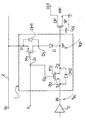
- the drawing shows a schematical view of a holding circuit according to this invention.
- the numeral 1 comprehensively and schematically designates a circuit for holding a field-effect power transistor MP of the MOS (Metal-Oxide Semiconductor) type in a conduction stated on the occurrence of a power outage.
- MOS Metal-Oxide Semiconductor
- That transistor MP is of the n-channel type and conventionally includes a source terminal SP connected to ground, and a drain terminal DP which forms an output terminal OUT for the circuit 1 and intended for connection to an external load, such as an electric motor not shown because of conventional design.
- the power transistor MP further includes a gate terminal GP having an inherent gate capacitance CGS.
- the circuit 1 is connected to an electric power supply line 2, in turn connected to a positive supply pole VA.
- the circuit 1 comprises a first transistor M1 of the p-channel MOS type having its source terminal S1 connected to the line 2, and its drain terminal D1 connected to the gate GP of the transistor MP via a diode D.
- the transistor M1 further includes an intrinsic diode DM1 connected between the drain D1 and the source S1, as well as a gate terminal C1 connected to an input terminal A of the circuit 1 and intended for receiving a signal commanding the make state of the transistor MP.
- a second transistor M2 of the n-channel MOS type be arranged to have its gate terminal G2 connected to the gate G1 of the transistor M1 and its drain terminal D2 connected to the gate GP of the power transistor MP.
- That second transistor M2 also has the source S2 and substrate B2 terminals connected to each other and and to an input terminal IN which is connected to the output of a driver circuit 3 external of the circuit 1 and operative to drive the transistor MP.
- the transistor M2 is in turn provided with an intrinsic diode DM2 connected between the source S2 and drain D2 terminals; in addition, the transistor M2 should be sized to have a negligible serial resistance compared to the serial resistance of the driver 3.
- the circuit 1 of this invention operates as follows.
- the transistor M2 is instead conducting if the supply voltage VA is higher than the voltage VIN at the input terminal IN for the threshold voltage VTH2 of the transistor M2. Even if the threshold voltage VTH2 is greater than a diode voltage drop, the driver 3 would drive the gate GP of the transistor MP and all the output voltage VIN delivered to that gate less the voltage drop across the intrinsic diode DM2.
- the transistor M2 is put in an off state in that it presents a positive or no voltage VIN at the source and zero voltage at the gate G2.
- the transistor M2 is still in a non-conducting state, and the transistor M1 could provide a route for discharging the capacitor CGS of the power transistor through the diode DM1. Actually, since the voltage VA is lower than the voltage VGP at the gate of the transistor MP, the diode D would be reverse biased and inhibit discharge of the gate capacitor of the power transistor MP.
- the sole current leakouts are those of the diode D and transistor M1, having the intrinsic diode DM1, which would rather disconnect the driver 3 from the gate capacitor of the power transistor. Accordingly, on the occurrence of the supply voltage VA drop, the gate of the power transistor is automatically isolated from all the components of the circuit 1, and holds that transistor in a permanently conducting state.
- the circuit of this invention solves, therefore, the technical problem and affords a number of advantages, an outstanding one being that the very inherent gate capacitance of the power transistor is utilized to hold it in conduction on the occurrence of a drop in the voltage supply.
- the circuit of this invention is made up of peculiarly low number of components, and makes provisions unnecessary to cancel leakage currents of the drivers in the absence of power supply.
- the circuit can be driven, in the absence of power supply, in an extremely simple way, since the input impedance of the make terminal A is almost infinitive and receives under that condition a signal having a low logic value.
Landscapes
- Electronic Switches (AREA)
- Protection Of Generators And Motors (AREA)
- Power Conversion In General (AREA)
Abstract
Description
- This invention relates to a circuit for holding a MOS transistor, in particular a power transistor, in a conduction state on the occurrence of an outage in the voltage supply, being of a type which comprises a first N-channel MOS transistor having its source terminal connected to a line of said voltage supply and its drain terminal connected to the gate of said power transistor.
- As is known, MOS power transistors are widely employed to connect and control electric loads, in particular electric motors.
- Should a drop off occur in the voltage supply, the phases of the electric motor must be connected to ground by closing switches. Such switches may comprise the above-noted MOS power transistors which, in order to operate as closed switches, are to be held in a conducting state even if the electric power supply has failed.
- To meet that demand, the prior art has proposed a circuit arrangement as described herein below.
- Each power transistor is connected to a make circuit which comprises a MOS transistor having its source terminal connected to an electric supply line via a diode, and its drain terminal connected to the gate of the power transistor. The gate terminal of that MOS transistor is intended to receive a make signal for the power transistor, which transistor receives, in turn, on its gate terminal a signal from the output of a so-called driver.
- Also provided is a large capacitance connected between the source of the make MOS transistor and ground. This capacitance makes up for current leakouts from the make circuit on the occurrence of a drop-off in the electric supply, as well as for current leakouts from the driver which, when receiving no power, behaves at its output as a circuit shorting out to ground.
- This prior technical approach, while substantially achieving its objective, has the serious drawback that the value of said capacitance must be high, thereby its incorporation to the integrated circuit forming the make circuit is unthinkable, on account of enhanced costs and space requirements.
- The technical problem that underlies this invention is to provide a circuit which has such design and performance characteristics as to allow of a MOS power transistor to be held in a conducting state on a failure of the electric power supply to thereby obviate the drawback with which the prior art is beset.
- This problem is solved by a circuit of the kind specified hereinabove being characterized in that it comprises a diode connected between the drain of the first transistor and the gate of the power transistor, and a second transistor of the MOS type having its gate connected to the gate of the first transistor and its drain connected to the gate of the power transistor.
- The features and advantages of a circuit according to the invention will be more clearly apparent from the following detailed description of an embodiment thereof, to be taken by way of illustration only in conjunction with the accompanying drawing.
- The drawing shows a schematical view of a holding circuit according to this invention.
- With reference to the drawing, the numeral 1 comprehensively and schematically designates a circuit for holding a field-effect power transistor MP of the MOS (Metal-Oxide Semiconductor) type in a conduction stated on the occurrence of a power outage.
- That transistor MP is of the n-channel type and conventionally includes a source terminal SP connected to ground, and a drain terminal DP which forms an output terminal OUT for the circuit 1 and intended for connection to an external load, such as an electric motor not shown because of conventional design.
- The power transistor MP further includes a gate terminal GP having an inherent gate capacitance CGS.
- The circuit 1 is connected to an electric power supply line 2, in turn connected to a positive supply pole VA.
- In detail, the circuit 1 comprises a first transistor M1 of the p-channel MOS type having its source terminal S1 connected to the line 2, and its drain terminal D1 connected to the gate GP of the transistor MP via a diode D.
- The transistor M1 further includes an intrinsic diode DM1 connected between the drain D1 and the source S1, as well as a gate terminal C1 connected to an input terminal A of the circuit 1 and intended for receiving a signal commanding the make state of the transistor MP.
- Advantageously, it is also contemplated that a second transistor M2 of the n-channel MOS type be arranged to have its gate terminal G2 connected to the gate G1 of the transistor M1 and its drain terminal D2 connected to the gate GP of the power transistor MP.
- That second transistor M2 also has the source S2 and substrate B2 terminals connected to each other and and to an input terminal IN which is connected to the output of a driver circuit 3 external of the circuit 1 and operative to drive the transistor MP.
- The transistor M2 is in turn provided with an intrinsic diode DM2 connected between the source S2 and drain D2 terminals; in addition, the transistor M2 should be sized to have a negligible serial resistance compared to the serial resistance of the driver 3.
- The circuit 1 of this invention operates as follows.
- Assuming in operation a starting condition whereby power is supplied on the line 2, there may occur either of two cases.
- The voltage V at the input terminal A is equal to the supply voltage VA (V = VA). It follows that the voltage drop VGS between the gate and the source of the transistor M1 will be 0 Volts, and accordingly that transistor will be in an off state. The transistor M2 is instead conducting if the supply voltage VA is higher than the voltage VIN at the input terminal IN for the threshold voltage VTH2 of the transistor M2. Even if the threshold voltage VTH2 is greater than a diode voltage drop, the driver 3 would drive the gate GP of the transistor MP and all the output voltage VIN delivered to that gate less the voltage drop across the intrinsic diode DM2.
- The voltage V at the terminal A is nought (V = 0 Volts), the transistor M1 is conducting and, through the diode D, charges the gate capacitor of the transistor MP, thereby the latter will be in turn conducting.
- At the same time, the transistor M2 is put in an off state in that it presents a positive or no voltage VIN at the source and zero voltage at the gate G2.
- Now, a third possible operational case presents itself.
- This is the case in which there is no supply voltage on the line 2 (VA = 0), and the voltage V is zero also at the terminal A.
- Inasmuch as that operating condition follows in time the Case 2 just discussed, the gate capacitor of the transistor MP will be charged, and that transistor keep conducting.
- The transistor M2 is still in a non-conducting state, and the transistor M1 could provide a route for discharging the capacitor CGS of the power transistor through the diode DM1. Actually, since the voltage VA is lower than the voltage VGP at the gate of the transistor MP, the diode D would be reverse biased and inhibit discharge of the gate capacitor of the power transistor MP.
- To summarize, the sole current leakouts are those of the diode D and transistor M1, having the intrinsic diode DM1, which would rather disconnect the driver 3 from the gate capacitor of the power transistor. Accordingly, on the occurrence of the supply voltage VA drop, the gate of the power transistor is automatically isolated from all the components of the circuit 1, and holds that transistor in a permanently conducting state.
- The circuit of this invention solves, therefore, the technical problem and affords a number of advantages, an outstanding one being that the very inherent gate capacitance of the power transistor is utilized to hold it in conduction on the occurrence of a drop in the voltage supply.
- The circuit of this invention is made up of peculiarly low number of components, and makes provisions unnecessary to cancel leakage currents of the drivers in the absence of power supply.
- The circuit can be driven, in the absence of power supply, in an extremely simple way, since the input impedance of the make terminal A is almost infinitive and receives under that condition a signal having a low logic value.
Claims (1)
- A circuit (1) for holding a MOS power transistor (MP) in a conduction state on the occurrence of an outage in the voltage supply (VA), being of a type comprising a first n-channel MOS transistor (M1) having its source terminal (S1) connected to a line (2) of said voltage supply (VA) and its drain terminal (D2) connected to the gate (GP) of said power transistor (MP), characterized in that it comprises a diode (D) connected between the drain (D1) of the first transistor and the gate (GP) of the power transistor, and a second transistor (M2) of the MOS type having its gate (G2) connected to the gate (G1) of the first transistor (M1) and its drain connected to the gate (GP) of the power transistor (MP).
Applications Claiming Priority (2)
| Application Number | Priority Date | Filing Date | Title |
|---|---|---|---|
| IT8723162A IT1224644B (en) | 1987-12-22 | 1987-12-22 | CIRCUIT FOR MAINTAINING A MOS TRANSISTOR IN CONDUCT WITHOUT POWER SUPPLY VOLTAGE. |
| IT2316287 | 1987-12-22 |
Publications (3)
| Publication Number | Publication Date |
|---|---|
| EP0321702A2 true EP0321702A2 (en) | 1989-06-28 |
| EP0321702A3 EP0321702A3 (en) | 1990-08-22 |
| EP0321702B1 EP0321702B1 (en) | 1993-10-13 |
Family
ID=11204432
Family Applications (1)
| Application Number | Title | Priority Date | Filing Date |
|---|---|---|---|
| EP88119207A Expired - Lifetime EP0321702B1 (en) | 1987-12-22 | 1988-11-18 | A circuit for holding a mos transistor in a conduction state in a voltage supply outage situation |
Country Status (5)
| Country | Link |
|---|---|
| US (1) | US4914316A (en) |
| EP (1) | EP0321702B1 (en) |
| JP (1) | JP2770969B2 (en) |
| DE (1) | DE3884925T2 (en) |
| IT (1) | IT1224644B (en) |
Cited By (2)
| Publication number | Priority date | Publication date | Assignee | Title |
|---|---|---|---|---|
| EP0468650A1 (en) * | 1990-07-13 | 1992-01-29 | Illinois Tool Works Inc. | Solid state switch with last state memory |
| WO2002075924A3 (en) * | 2001-03-20 | 2002-12-27 | Koninkl Philips Electronics Nv | Circuit and method for controlling a dynamic, bi-directional high voltage analog switch and ultrasound examination apparatus equipped with such a circuit |
Families Citing this family (9)
| Publication number | Priority date | Publication date | Assignee | Title |
|---|---|---|---|---|
| US5065047A (en) * | 1989-03-27 | 1991-11-12 | Nissan Motor Co., Ltd. | Digital circuit including fail-safe circuit |
| US5148047A (en) * | 1990-06-11 | 1992-09-15 | Motorola, Inc. | CMOS bus driver circuit with improved speed |
| US5130562A (en) * | 1990-08-31 | 1992-07-14 | Advanced Micro Devices, Inc. | Integrated power-sense circuit |
| US6031408A (en) * | 1991-09-20 | 2000-02-29 | Motorola, Inc. | Square-law clamping circuit |
| JP3545049B2 (en) * | 1993-06-22 | 2004-07-21 | エスティーマイクロエレクトロニクス,インコーポレイテッド | Back electromotive force rectified voltage at power supply energy failure |
| JPH07129538A (en) * | 1993-10-29 | 1995-05-19 | Mitsubishi Denki Semiconductor Software Kk | Semiconductor integrated circuit |
| DE69328623T2 (en) * | 1993-11-30 | 2001-02-08 | Stmicroelectronics S.R.L., Agrate Brianza | Stable reference voltage generator circuit |
| FR2738422B1 (en) * | 1995-08-31 | 1997-10-24 | Suisse Electronique Microtech | POLARIZATION CIRCUIT FOR SETTING THE AVERAGE LEVEL OF AN ALTERNATING VOLTAGE |
| EP1415398A2 (en) * | 2001-07-25 | 2004-05-06 | Koninklijke Philips Electronics N.V. | Output driver equipped with a sensing resistor for measuring the current in the output driver |
Family Cites Families (7)
| Publication number | Priority date | Publication date | Assignee | Title |
|---|---|---|---|---|
| US3700968A (en) * | 1971-01-20 | 1972-10-24 | Messerschmitt Boelkow Blohm | Electric fuse circuit |
| JPS52153630A (en) * | 1976-06-16 | 1977-12-20 | Matsushita Electric Ind Co Ltd | Semiconductor memory device |
| FR2445642A1 (en) * | 1978-12-29 | 1980-07-25 | Radiotechnique Compelec | SAFETY ARRANGEMENT IN THE EVENT OF A DROP IN CONTINUOUS SUPPLY VOLTAGE |
| US4317056A (en) * | 1980-03-24 | 1982-02-23 | Gte Products Corporation | Voltage monitoring and indicating circuit |
| US4663547A (en) * | 1981-04-24 | 1987-05-05 | General Electric Company | Composite circuit for power semiconductor switching |
| US4737667A (en) * | 1986-03-11 | 1988-04-12 | Siemens Aktiengesellschaft | Driving circuitry for a MOSFET having a source load |
| DE3613943A1 (en) * | 1986-04-24 | 1987-10-29 | Bosch Gmbh Robert | ELECTRONIC DEVICE POWERED FROM A ACCUMULATOR AND SWITCHED ON AND OFF WITH A KEY SWITCH |
-
1987
- 1987-12-22 IT IT8723162A patent/IT1224644B/en active
-
1988
- 1988-11-18 EP EP88119207A patent/EP0321702B1/en not_active Expired - Lifetime
- 1988-11-18 DE DE88119207T patent/DE3884925T2/en not_active Expired - Fee Related
- 1988-12-12 US US07/283,232 patent/US4914316A/en not_active Expired - Lifetime
- 1988-12-22 JP JP63322259A patent/JP2770969B2/en not_active Expired - Fee Related
Cited By (2)
| Publication number | Priority date | Publication date | Assignee | Title |
|---|---|---|---|---|
| EP0468650A1 (en) * | 1990-07-13 | 1992-01-29 | Illinois Tool Works Inc. | Solid state switch with last state memory |
| WO2002075924A3 (en) * | 2001-03-20 | 2002-12-27 | Koninkl Philips Electronics Nv | Circuit and method for controlling a dynamic, bi-directional high voltage analog switch and ultrasound examination apparatus equipped with such a circuit |
Also Published As
| Publication number | Publication date |
|---|---|
| IT1224644B (en) | 1990-10-18 |
| IT8723162A0 (en) | 1987-12-22 |
| EP0321702A3 (en) | 1990-08-22 |
| US4914316A (en) | 1990-04-03 |
| DE3884925T2 (en) | 1994-02-03 |
| JP2770969B2 (en) | 1998-07-02 |
| DE3884925D1 (en) | 1993-11-18 |
| JPH024007A (en) | 1990-01-09 |
| EP0321702B1 (en) | 1993-10-13 |
Similar Documents
| Publication | Publication Date | Title |
|---|---|---|
| US4736121A (en) | Charge pump circuit for driving N-channel MOS transistors | |
| US5892371A (en) | Gate oxide voltage limiting devices for digital circuits | |
| US10840898B2 (en) | Semiconductor device and electronic control device | |
| EP0442688A2 (en) | Switching circuit | |
| US20040217653A1 (en) | Supply selection circuit with programmable hysteresis | |
| US4698530A (en) | Power switch for dual power supply circuit | |
| EP2071724A1 (en) | Power supply control circuit | |
| EP2293446B1 (en) | Coupling circuit, driver circuit and method for controlling a coupling circuit | |
| US4914316A (en) | Circuit for holding a MOS transistor in a conduction state in a voltage supply outage situation | |
| CN108781078B (en) | Power supply control device | |
| EP0086090A1 (en) | Drive circuit for capacitive loads | |
| JPH0769749B2 (en) | DC power supply circuit | |
| US20040264084A1 (en) | Polarity protection implemented with a mosfet | |
| SE467854B (en) | DRIVING CIRCUIT LIVES N-CHANNEL POWER EQUIPMENT TRANSISTORS | |
| US20210351177A1 (en) | Semiconductor device | |
| EP0130079B1 (en) | Mos high current output buffer | |
| US5280201A (en) | Semiconductor logic circuit apparatus | |
| US7084697B2 (en) | Charge pump circuit capable of completely cutting off parasitic transistors | |
| EP1183780B1 (en) | Electronic circuit provided with a digital driver for driving a capacitive load | |
| US5959494A (en) | High-voltage switch control | |
| US12113524B2 (en) | Active bootstrapping drivers | |
| EP0328168A1 (en) | Push-pull output circuit which is free from hot carrier stress | |
| EP1001537A2 (en) | Control circuit | |
| US7319359B2 (en) | High current charge pump for intelligent power switch drive | |
| JP3681731B2 (en) | Drive circuit |
Legal Events
| Date | Code | Title | Description |
|---|---|---|---|
| PUAI | Public reference made under article 153(3) epc to a published international application that has entered the european phase |
Free format text: ORIGINAL CODE: 0009012 |
|
| AK | Designated contracting states |
Kind code of ref document: A2 Designated state(s): DE FR GB NL SE |
|
| PUAL | Search report despatched |
Free format text: ORIGINAL CODE: 0009013 |
|
| AK | Designated contracting states |
Kind code of ref document: A3 Designated state(s): DE FR GB NL SE |
|
| 17P | Request for examination filed |
Effective date: 19900926 |
|
| 17Q | First examination report despatched |
Effective date: 19920225 |
|
| GRAA | (expected) grant |
Free format text: ORIGINAL CODE: 0009210 |
|
| AK | Designated contracting states |
Kind code of ref document: B1 Designated state(s): DE FR GB NL SE |
|
| REF | Corresponds to: |
Ref document number: 3884925 Country of ref document: DE Date of ref document: 19931118 |
|
| ET | Fr: translation filed | ||
| PLBE | No opposition filed within time limit |
Free format text: ORIGINAL CODE: 0009261 |
|
| STAA | Information on the status of an ep patent application or granted ep patent |
Free format text: STATUS: NO OPPOSITION FILED WITHIN TIME LIMIT |
|
| 26N | No opposition filed | ||
| EAL | Se: european patent in force in sweden |
Ref document number: 88119207.4 |
|
| REG | Reference to a national code |
Ref country code: FR Ref legal event code: D6 |
|
| PGFP | Annual fee paid to national office [announced via postgrant information from national office to epo] |
Ref country code: SE Payment date: 20011106 Year of fee payment: 14 |
|
| PGFP | Annual fee paid to national office [announced via postgrant information from national office to epo] |
Ref country code: NL Payment date: 20011129 Year of fee payment: 14 |
|
| REG | Reference to a national code |
Ref country code: GB Ref legal event code: IF02 |
|
| PGFP | Annual fee paid to national office [announced via postgrant information from national office to epo] |
Ref country code: FR Payment date: 20021108 Year of fee payment: 15 |
|
| PGFP | Annual fee paid to national office [announced via postgrant information from national office to epo] |
Ref country code: GB Payment date: 20021113 Year of fee payment: 15 |
|
| PG25 | Lapsed in a contracting state [announced via postgrant information from national office to epo] |
Ref country code: SE Free format text: LAPSE BECAUSE OF NON-PAYMENT OF DUE FEES Effective date: 20021119 |
|
| PGFP | Annual fee paid to national office [announced via postgrant information from national office to epo] |
Ref country code: DE Payment date: 20021121 Year of fee payment: 15 |
|
| PG25 | Lapsed in a contracting state [announced via postgrant information from national office to epo] |
Ref country code: NL Free format text: LAPSE BECAUSE OF NON-PAYMENT OF DUE FEES Effective date: 20030601 |
|
| EUG | Se: european patent has lapsed | ||
| NLV4 | Nl: lapsed or anulled due to non-payment of the annual fee |
Effective date: 20030601 |
|
| PG25 | Lapsed in a contracting state [announced via postgrant information from national office to epo] |
Ref country code: GB Free format text: LAPSE BECAUSE OF NON-PAYMENT OF DUE FEES Effective date: 20031118 |
|
| PG25 | Lapsed in a contracting state [announced via postgrant information from national office to epo] |
Ref country code: DE Free format text: LAPSE BECAUSE OF NON-PAYMENT OF DUE FEES Effective date: 20040602 |
|
| GBPC | Gb: european patent ceased through non-payment of renewal fee |
Effective date: 20031118 |
|
| PG25 | Lapsed in a contracting state [announced via postgrant information from national office to epo] |
Ref country code: FR Free format text: LAPSE BECAUSE OF NON-PAYMENT OF DUE FEES Effective date: 20040730 |
|
| REG | Reference to a national code |
Ref country code: FR Ref legal event code: ST |