EP0319980A2 - Apparatus for controlling a power converter - Google Patents
Apparatus for controlling a power converter Download PDFInfo
- Publication number
- EP0319980A2 EP0319980A2 EP88120549A EP88120549A EP0319980A2 EP 0319980 A2 EP0319980 A2 EP 0319980A2 EP 88120549 A EP88120549 A EP 88120549A EP 88120549 A EP88120549 A EP 88120549A EP 0319980 A2 EP0319980 A2 EP 0319980A2
- Authority
- EP
- European Patent Office
- Prior art keywords
- phase
- voltage
- signal
- output
- power converter
- Prior art date
- Legal status (The legal status is an assumption and is not a legal conclusion. Google has not performed a legal analysis and makes no representation as to the accuracy of the status listed.)
- Granted
Links
- 238000010304 firing Methods 0.000 claims description 21
- 230000001360 synchronised effect Effects 0.000 claims description 7
- 229910001219 R-phase Inorganic materials 0.000 description 17
- 230000018199 S phase Effects 0.000 description 4
- 230000005415 magnetization Effects 0.000 description 4
- 239000003990 capacitor Substances 0.000 description 3
- 238000010276 construction Methods 0.000 description 3
- 238000010586 diagram Methods 0.000 description 2
- 238000000034 method Methods 0.000 description 1
- 238000010791 quenching Methods 0.000 description 1
- 238000006467 substitution reaction Methods 0.000 description 1
Images
Classifications
-
- H—ELECTRICITY
- H02—GENERATION; CONVERSION OR DISTRIBUTION OF ELECTRIC POWER
- H02M—APPARATUS FOR CONVERSION BETWEEN AC AND AC, BETWEEN AC AND DC, OR BETWEEN DC AND DC, AND FOR USE WITH MAINS OR SIMILAR POWER SUPPLY SYSTEMS; CONVERSION OF DC OR AC INPUT POWER INTO SURGE OUTPUT POWER; CONTROL OR REGULATION THEREOF
- H02M7/00—Conversion of ac power input into dc power output; Conversion of dc power input into ac power output
- H02M7/42—Conversion of dc power input into ac power output without possibility of reversal
- H02M7/44—Conversion of dc power input into ac power output without possibility of reversal by static converters
- H02M7/48—Conversion of dc power input into ac power output without possibility of reversal by static converters using discharge tubes with control electrode or semiconductor devices with control electrode
- H02M7/505—Conversion of dc power input into ac power output without possibility of reversal by static converters using discharge tubes with control electrode or semiconductor devices with control electrode using devices of a thyratron or thyristor type requiring extinguishing means
- H02M7/515—Conversion of dc power input into ac power output without possibility of reversal by static converters using discharge tubes with control electrode or semiconductor devices with control electrode using devices of a thyratron or thyristor type requiring extinguishing means using semiconductor devices only
- H02M7/525—Conversion of dc power input into ac power output without possibility of reversal by static converters using discharge tubes with control electrode or semiconductor devices with control electrode using devices of a thyratron or thyristor type requiring extinguishing means using semiconductor devices only with automatic control of output waveform or frequency
- H02M7/527—Conversion of dc power input into ac power output without possibility of reversal by static converters using discharge tubes with control electrode or semiconductor devices with control electrode using devices of a thyratron or thyristor type requiring extinguishing means using semiconductor devices only with automatic control of output waveform or frequency by pulse width modulation
Definitions
- This invention relates to an apparatus for controlling a power converter, which is adapted to control, in accordance with the PWM system, a power converter for system interconnection interposed between the d.c. power source and the a.c. system to adjust interchange power therebetween.
- Power converters for system interconnection of this kind may have an inverter operating mode used in supplying power from the d.c. power source to the a.c. system and a rectifier operating mode used in supplying power from the a.c. system to the d.c. power in a manner opposite to the above.
- the power converter is operated in the rectifier operating mode the amplitude of voltage V in is smaller than that of voltage V sy and the phase of voltage V in lags that of voltage V sy .
- the power converter dissipates lagging reactive power Q and transmits effective power P from the a.c. system to the d.c. power source.
- the power converter dissipates lagging reactive power Q and transmits effective power P from the d.c. power source to the a.c. system.
- the power converter When the effective value of the voltage V in satisfies the condition expressed by the following equation with respect to the effective value of the voltage V sy , V in ⁇ V sy /cos ⁇ (3) the power converter operates as a capacitor and transmits effective power from the a.c. system to the d.c. power source.
- the phase difference angle ⁇ is positive as apparent from the above equations (1) and (2) even in the case where the above equation (3) is satisfied, the power converter operates as a capacitor and transmits effective power from the d.c. power source to the a.c. system.
- the effective power P and the reactive power Q can be adjusted.
- the three phases are not necessarily balanced with each other in an ordinary a.c. system voltage.
- three phases are unbalanced, for example, in a form such that amplitudes are different from each other in respective R, S and T phases.
- the above-described power converter can interchange the effective and reactive powers between the a.c. system and the d.c. power source.
- the effective and reactive powers with three phases being as a lump under condition where amplitudes of the output a.c. voltage are different from each other in the three phases take predetermined values, respectively.
- an object of this invention is to provide an apparatus for controlling a power converter interposed between the d.c. power source and the a.c. system to interchange power therebetween, which is capable of eliminating the above-described overcurrent or d.c. polarized magnetization based on imbalance of the a.c. system voltage or unevenness between element characteristics.
- an apparatus for controlling a power converter comprising synchronous detector means for detecting a phase of an a.c. system voltage to output it as a synchronizing signal, output voltage phase signal generator means for determining a phase of an output a.c. voltage from a phase difference angle adjustment signal for determination of a phase difference between the a.c. system voltage and the output a.c. voltage and the synchronizing signal from the synchronous detector means to output it as an output voltage phase signal, phase voltage amplitude signal generator means for obtaining a voltage amplitude adjustment signal for determining an amplitude per phase of the output a.c.
- firing signal generator means for determining energization periods of respective controllable rectifier elements constituting the power converter from the voltage phase signal on the basis of the output voltage phase signal generator circuit and the phase voltage amplitude signal from the phase voltage amplitude signal generator circuit.
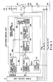
- a voltage controlled type inverter 11 generally used for system interconnection as a power converter controlled by a control apparatus according to this invention is shown.
- an inverter main circuit 10 is constituted.
- a d.c. power source 20 is interconnected with an a.c. system 50 through the inverter main circuit 10, an interconnecting reactor 30 and an interconnecting transformer 40.
- Fig. 2 shows the circuit construction of the voltage controlled inverter 11 constituting the inverter main circuit 10.
- This circuit arrangement is provided with a pair of positive and negative d.c. terminals PT and NT, and three-phase a.c. terminals R, S and T.
- the inverter 11 is composed of six controllable rectifier elements GU, GV, GW, GX, GY and GZ which are three-phase bridge connected, and six free-wheeling diodes DU, DV, DW, DX, DY and DZ connected in inverse-parallel with these controllable rectifier elements, respectively.
- Such controllable rectifier elements GU to GZ are each comprised of an element of the self-quenching type, such as, for example, a gate turn off thyristor (GTO).
- GTO gate turn off thyristor
- the interchange of power in the system construction of Fig. 1 is controlled by the inverter 11.
- the voltage of the a.c. system 50 i.e., system voltage V sy is detected by a potential transformer (which will be referred to as "PT" hereinafter) 61
- the voltage of the d.c. power source 20, i.e., d.c. voltage V dc is detected by a d.c. voltage detector (which will be referred to as "VD” hereinafter)
- output a.c. currents I r , I s and I t of respective phases of the inverter 11 are detected by a current transformer (which will be referred to as a "CT” hereinafter) 63.
- CT current transformer
- a power control unit 8 In order to form a control signal for adjusting an effective power P and a reactive power Q flowing into the a.c. system 50, a power control unit 8 is provided.
- the power control unit 8 calculates a modulation factor signal M f for voltage adjustment corresponding to the modulation factor M, and a phase difference angle signal ⁇ c corresponding to a phase difference angle ⁇ in accordance with the above equations (5) and (6) for the purpose of allowing the inverter 11 to interchange predetermined effective and reactive powers P and Q on the basis of the system voltage V sy (phase voltages V r , V s , V t ) and the d.c. voltage V dc respectively detected by PT 61 and VD 62.
- the power control unit 8 calculates correction modulation factor signals M r , M s and M t of respective phases for adjusting output voltage amplitudes of respective phases on the basis of respective phase alternative currents I r , I s and I t detected by the CT 63 or respective phase voltages V r , V s and V t of the system. Thus, the power control unit 8 sends the respective values obtained by calculation to the firing control unit 100.
- d.c. components included in the alternative currents I r , I s and I t of respective phases are detected, whereby correction modulation factor signals M r , M s and M t are determined so as to suppress such d.c. components.
- alternative currents I r , I s and I t are respectively integrated per cycle of the a.c. voltage to assume these three integrated values as correction modulation factor signals M r , M s and M t , respectively.
- one of three correction modulation factor signals may be set to a fixed value.
- the firing control unit 100 is provided with a synchronous detector circuit 110, a voltage phase signal generator circuit 120, a firing signal generator circuit 130, and a circuit 140 for producing a voltage amplitude signal per each phase (hereinafter simply referred to as a phase voltage amplitude signal generator circuit 140).
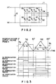
- the firing signal generator circuit 130 is comprised of a triangular wave generator circuit 131, a firing timing determination circuit 132, and a firing phase determination circuit 133.
- the triangular wave generator circuit 131 is a circuit to generate triangular wave signals TRI with 60 degrees being its period as shown in Fig. 3.
- the energization periods of respective controllable reactifier elements GU, GV, GW, GX, GY, and GZ are determined with the triangular wave signal TRI being as a reference.
- the synchronous detector circuit 110 obtains a system voltage V sy from PT 61 to detect the phase of the system voltage, thus to output a system phase signal SCLK.
- the voltage phase signal generator circuit 120 receives a phase difference angle signal ⁇ c from the power control unit 8 to send, to the firing signal generator circuit 130, an output voltage phase signal ⁇ comprised of a digital signal such that a phase difference angle between the output voltage of the inverter 11 and the voltage of the a.c.
- the output voltage phase signal ⁇ consists of a phase-judgement phase signal ⁇ h indicating a period of 360 degrees every 60 degrees with the R-phase output voltage being used as a reference, and a 60° period phase signal ⁇ j repeating from zero count to a predetermined count value every period of 60 degrees.
- the phase judgement phase signal ⁇ h may be prepared by a hexanary counter circuit repeating from 0 up to 5, and is assumed to have a relationship of Table 1 shown below between the phase-judgement phase signal ⁇ h and the phase ⁇ of the inverter R-phase output voltage.
- Table 1 Phase-Judgement Phase Signal ⁇ h Phase ⁇ of Inverter Output Voltage R-Phase 0 0° ⁇ 60° 1 60° ⁇ 120° 2 120° ⁇ 180° 3 180° ⁇ 240° 4 240° ⁇ 300° 5 300° ⁇ 360°
- the output voltage phase signal ⁇ consists of a phase-judgement phase signal ⁇ h and 60° period phase signal ⁇ j , and is in such a form to express the phase ⁇ of the R-phase output voltage of the inverter as a digital signal.
- the phase voltage amplitude signal generator circuit 140 inputs a phase-judgement phase signal ⁇ h from the voltage phase signal generator circuit 120 to output a voltage amplitude signal per phase denoted by M p (hereinafter simply referred to as a phase voltage amplitude signal M p ) to the firing signal generator circuit 130 at the time when the phase-judgement phase signal ⁇ h changes.
- M p voltage amplitude signal per phase denoted by M p
- the relationship between the phase voltage amplitude signal M p output from the phase voltage signal generator circuit 140 at the time when the phase-judgement phase signal ⁇ h varies and the phase-judgement phase signal ⁇ h is shown in Table 2.
- the phase voltage amplitude signal M p maintains the value when the phase-judgement phase signal ⁇ h changes last as long as the phase-judgement phase signal ⁇ h does not change.
- the phase voltage amplitude signal M p is varied as shown in Table 3 every 60 degrees of the phase of the R-phase output voltage of the inverter.
- the triangular wave generator circuit 131 within the firing signal generator circuit 130 inputs a 60° period phase signal ⁇ j from the voltage phase signal generator circuit 120 to output a triangular wave signal TRI to the firing timing determination circuit 132.
- a triangular wave signal TRI triangular waves each corresponding to an isosceles triangle with the phase angle of 30 degrees of the 60° period as a center are repeatedly output every 60° periods of the R-phase output voltage of the inverter 11, i.e., at periods of 60°, as shown in Fig. 3.
- the triangular wave signal TRI has a positive gradient corresponding to those count values, and from the time of 1023 counts of the 60° period phase signal ⁇ j up to the time of 2047 counts thereof, the triangular wave signal TRI has a negative gradient corresponding to from 1023 down to 0 counts.
- the firing timing determination circuit 132 determines the timing for controlling the energization periods of respective controllable rectifier elements of the inverter 11 on the basis of the phase voltage amplitude signal M p from the phase voltage signal generator circuit 140 and the triangular wave signal TRI from the triangular wave generator circuit 131 in accordance with the time sequence shown in Fig. 3.
- a method of generating timing signals for determining energization periods of the controllable rectifier elements GY and GV and the controllable rectifier elements GU and GX of the inverter 11 carried out when the R-phase output voltage phase ⁇ of the inverter 11 is at time periods of 0° ⁇ 60° and 60° ⁇ 120°, i.e., the phase-judgement phase signal ⁇ h represents "0" and "1" will be described with reference to Fig. 3.
- signal M y is output as the phase voltage amplitude signal M p .
- the signal M y and the triangular wave signal TRI are compared with each other to output a signal TIM indicating the times a1 and a2 at which both signals are equal to each other.
- the firing-phase determination circuit 133 determines the energization periods on the basis of the signal TIM obtained from the firing timing determination circuit 132 at the times of a1 and a2 and the output voltage phase signal ⁇ from the voltage phase signal generator circuit 120 so that the controllable rectifier elements GU and GW are energized and the controllable rectifier elements GX and GZ are not energized because controllable rectifier elements except for the controllable rectifier elements GV and GY of controllable rectifier elements of the inverter 11 are such that phase-judgement signal ⁇ h of the digital phase signal ⁇ represents "0".
- signal M u is output as the phase voltage amplitude signal M p .
- the signal M u and the triangular wave signal TRI are compared with each other to output a signal TIM indicating the times b1 and b2 at which both signals are equal to each other to the firing-phase determination circuit 133.
- the firing-phase determination circuit 133 determines, as shown in Table 3, energization periods except for the controllable rectifier elements GU and GX of controllable rectifier elements of the inverter 11 on the basis of the signal TIM obtained from the firing timing determination circuit 132 at the times of b1 and b2 and the output voltage phase signal ⁇ from the voltage phase signal generator circuit 120.
- the firing-phase determination circuit 133 determines respective energization periods so that the controllable rectifier elements GV and GW are not energized and the controllable rectifier elements GY and GZ are energized because controllable rectifier elements except for the controllable rectifier elements GV and GY of controllable rectifier elements of the inverter 11 are such that the phase-judgement phase signal ⁇ h of the output voltage phase signal ⁇ represents "1".
- phase voltage amplitude signal M p of Table 3 takes respective values of M z , M v , M x and M w in dependence upon the phase-judgement phase signal ⁇ h .
- energization periods of respective controllable rectifier elements of the inverter 11 are determined.
- the difference between the control system of this invention and the conventional PWM control system resides in that the modulation factor M corresponding to the phase voltage amplitude signal M p of Fig. 3 is altered independent of the phase of the output voltage of the inverter 11 in the latter system.
- the modulation factor M corresponding to the phase voltage amplitude signal M p of Fig. 3 is altered independent of the phase of the output voltage of the inverter 11 in the latter system.
- the modulation factor M corresponding to the phase voltage amplitude signal M p of Fig. 3 is altered independent of the phase of the output voltage of the inverter 11 in the latter system.
- the modulation factor M corresponding to the phase voltage amplitude signal M p of Fig. 3 is altered independent of the phase of the output voltage of the inverter 11 in the latter system.
- the phase voltage amplitude signal M p by changing the phase voltage amplitude signal M p so that it becomes equal to signals M y , M u , M z , M v , M
- the control apparatus of Fig. 1 can control the amplitudes of the respective phase output voltages of the inverter 11 with regard to respective phases every positive or negative side of the amplitudes.
- this control apparatus can eliminate d.c. components produced in the output voltage energy respective phase. Accordingly, this makes it possible to allow currents flowing in respective controllable rectifier elements to be balanced to prevent d.c. polarized magnetization of the inter-connecting transformer 40, resulting in stable operation of the inverter 11.
- the inverter output voltage will be controlled per each phase.
- the relationship between the phase-voltage controlled and the phase voltage amplitude signal M p of the output voltage of the inverter 11 is as shown in the Table 5.
- a scheme is employed to output the modulation factor signal M f , and correction modulation factor signals M r , M s and M t per phase from the power control unit 8 to the phase voltage amplitude signal generator circuit 140.
- a scheme may be employed to output the phase voltage amplitude signals M y , M u , M z , M v , M x and M w of Table 3 or the phase voltage amplitude signals M r1 , M s1 and M t1 of Table 5 which are varied by the phase-judgement phase signal ⁇ h from the power control apparatus 8 to the phase voltage amplitude signal generator circuit 140.
- the phase voltage amplitude signal generator circuit 140 outputs, by the phase-judgement phase signal ⁇ h , these phase voltage amplitude signals M y , M u , M z , M v , M x and M w or the phase voltage amplitude signals M r1 , M s1 and M t1 , to the firing signal generator circuit 130.
- the apparatus for controlling a power converter is constructed to obtain a voltage amplitude adjustment signal for determining the voltage amplitudes per each phase of an a.c. voltage generated in the power converter to switch voltage amplitude adjustment signals every respective phase in accordance with an output voltage phase signal from the output voltage phase signal generator circuit to produce a phase voltage amplitude signal to determine energization periods of respective controllable rectifier elements constituting the power converter from the phase voltage amplitude signal and the output voltage phase signal, to thereby control the output voltage of the power converter per phase.
- this apparatus can correct imbalance between respective phases of the output alternative currents of the power converter, or suppress d.c. components included in output currents of respective phases.
Abstract
Description
- This invention relates to an apparatus for controlling a power converter, which is adapted to control, in accordance with the PWM system, a power converter for system interconnection interposed between the d.c. power source and the a.c. system to adjust interchange power therebetween.
- Power converters for system interconnection of this kind may have an inverter operating mode used in supplying power from the d.c. power source to the a.c. system and a rectifier operating mode used in supplying power from the a.c. system to the d.c. power in a manner opposite to the above.
- When it is assumed that a voltage on the a.c. side of a power converter is Vin, a voltage of the a.c. system is Vsy, a reactance between the d.c. power source and the a.c. system is X, and a phase difference angle between the voltage Vin and the voltage Vsy is Φ (which is positive when the phase of the voltage Vin leads the phase of the voltage Vsy), effective or active power P and reactive power Q processed in the power converter are respectively expressed as follows:
P = {(Vin·Vsy)/X}sinΦ (1)
Q = (Vin·Vsy·cosΦ - Vsy²)/X (2).
- Where the power converter is operated in the rectifier operating mode the amplitude of voltage Vin is smaller than that of voltage Vsy and the phase of voltage Vin lags that of voltage Vsy. Thus, the power converter dissipates lagging reactive power Q and transmits effective power P from the a.c. system to the d.c. power source. Moreover, as apparent from the above equations (1) and (2), even if the amplitude of voltage Vin is smaller than that of voltage Vsy, as long as the phase of voltage Vin leads that of voltage Vsy, the power converter dissipates lagging reactive power Q and transmits effective power P from the d.c. power source to the a.c. system.
- When the effective value of the voltage Vin satisfies the condition expressed by the following equation with respect to the effective value of the voltage Vsy,
Vin ≧ Vsy/cosΦ (3)
the power converter operates as a capacitor and transmits effective power from the a.c. system to the d.c. power source. When the phase difference angle Φ is positive as apparent from the above equations (1) and (2) even in the case where the above equation (3) is satisfied, the power converter operates as a capacitor and transmits effective power from the d.c. power source to the a.c. system. - When it is assumed that the voltage on the d.c. side of the power converter, i.e., the voltage of the d.c. power source is Vdc, modulation factor in the PWM control of the power converter is M (0≦M≦1), and k is a constant, the voltage Vin on the a.c. side of the power converter is expressed as follows:
Vin = k · Vdc · M (4).
- Substitution of the equation (4) into the equations (1) and (2) respectively gives:
P = Vsy(k·M·Vdc/X)sinΦ (5),and
Q = {Vsy(k·M·Vdc·cosΦ) - Vsy²}/X (6).
- As apparent from the above equations (5) and (6), by controlling the modulation factor M and/or the phase difference angle Φ by the power converter, the effective power P and the reactive power Q can be adjusted.
- Meanwhile, the three phases are not necessarily balanced with each other in an ordinary a.c. system voltage. There are many instances where three phases are unbalanced, for example, in a form such that amplitudes are different from each other in respective R, S and T phases. Even in the case where the a.c. system voltage is unbalanced as stated above, the above-described power converter can interchange the effective and reactive powers between the a.c. system and the d.c. power source. However, because the three phases of the a.c. sytem voltage are unbalanced, the effective and reactive powers with three phases being as a lump under condition where amplitudes of the output a.c. voltage are different from each other in the three phases take predetermined values, respectively. In this case, when the degree of imbalance becomes large, the output current of the converter of a specified phase will increase and therefore a current over an allowed current will flow in controllable rectifier elements of the specified phase. As a result, it becomes impossible to continue the operation of the converter.
- In addition to the above-described inconvenience, there is another inconvenience described below. Since there essentially exists unevenness in the characteristics of respective controllable rectifier elements even if the energization periods of respective controllable rectifier elements of the converter are determined, energization is not necessarily conducted as required by a designated energization period, so that there may be produced unevennesses between energization periods of respective controllable rectifier elements. Such unevennesses between energization periods of respective controllable rectifier elements cause the current on the a.c. side of the converter to produce d.c. components. The d.c. components mentioned above cause d.c. polarized magnetization in the interconnecting transformer ordinarily provided between the converter and the a.c. system, thus allowing the interconnecting transformer to over-heat, or otherwise extremely distorting an output current of the converter. When the occasion demands, there may occur a circumstance where a large peak current based on strain exceeds an allowed current value of the controllable rectifier element. Such circumstances make the operation of the converter impossible.
- Therefore, an object of this invention is to provide an apparatus for controlling a power converter interposed between the d.c. power source and the a.c. system to interchange power therebetween, which is capable of eliminating the above-described overcurrent or d.c. polarized magnetization based on imbalance of the a.c. system voltage or unevenness between element characteristics.
- In accordance with this invention, there is provided an apparatus for controlling a power converter comprising synchronous detector means for detecting a phase of an a.c. system voltage to output it as a synchronizing signal, output voltage phase signal generator means for determining a phase of an output a.c. voltage from a phase difference angle adjustment signal for determination of a phase difference between the a.c. system voltage and the output a.c. voltage and the synchronizing signal from the synchronous detector means to output it as an output voltage phase signal, phase voltage amplitude signal generator means for obtaining a voltage amplitude adjustment signal for determining an amplitude per phase of the output a.c. voltage to switch voltage amplitude adjustment signals of at least two phases in accordance with an output voltage phase signal for the output voltage phase signal generator circuit to output a signal obtained by switching as a phase voltage amplitude signal, and firing signal generator means for determining energization periods of respective controllable rectifier elements constituting the power converter from the voltage phase signal on the basis of the output voltage phase signal generator circuit and the phase voltage amplitude signal from the phase voltage amplitude signal generator circuit.
- In the accompanying drawings:
- Fig. 1 is a block diagram showing an embodiment of an apparatus for controlling a power converter according to this invention;
- Fig. 2 is a connection diagram showing the detailed construction of the converter shown in Fig. 1; and
- Fig. 3 is a time chart for explaining the function of the control apparatus shown in Fig. 1.
- In Fig. 1, a voltage controlled type inverter 11 generally used for system interconnection as a power converter controlled by a control apparatus according to this invention is shown. By the inverter 11 and d.c.
capacitor 12 connected on the d.c. input side thereof, an inverter main circuit 10 is constituted. A d.c.power source 20 is interconnected with ana.c. system 50 through the inverter main circuit 10, an interconnecting reactor 30 and an interconnectingtransformer 40. - Fig. 2 shows the circuit construction of the voltage controlled inverter 11 constituting the inverter main circuit 10. This circuit arrangement is provided with a pair of positive and negative d.c. terminals PT and NT, and three-phase a.c. terminals R, S and T. The inverter 11 is composed of six controllable rectifier elements GU, GV, GW, GX, GY and GZ which are three-phase bridge connected, and six free-wheeling diodes DU, DV, DW, DX, DY and DZ connected in inverse-parallel with these controllable rectifier elements, respectively. Such controllable rectifier elements GU to GZ are each comprised of an element of the self-quenching type, such as, for example, a gate turn off thyristor (GTO).
- The interchange of power in the system construction of Fig. 1 is controlled by the inverter 11. For controlling such interchange power, the voltage of the
a.c. system 50, i.e., system voltage Vsy is detected by a potential transformer (which will be referred to as "PT" hereinafter) 61, the voltage of the d.c.power source 20, i.e., d.c. voltage Vdc is detected by a d.c. voltage detector (which will be referred to as "VD" hereinafter), and output a.c. currents Ir, Is and It of respective phases of the inverter 11 are detected by a current transformer (which will be referred to as a "CT" hereinafter) 63. - In order to form a control signal for adjusting an effective power P and a reactive power Q flowing into the
a.c. system 50, apower control unit 8 is provided. Thepower control unit 8 calculates a modulation factor signal Mf for voltage adjustment corresponding to the modulation factor M, and a phase difference angle signal Φc corresponding to a phase difference angle Φ in accordance with the above equations (5) and (6) for the purpose of allowing the inverter 11 to interchange predetermined effective and reactive powers P and Q on the basis of the system voltage Vsy (phase voltages Vr, Vs, Vt) and the d.c. voltage Vdc respectively detected byPT 61 andVD 62. Further, thepower control unit 8 calculates correction modulation factor signals Mr, Ms and Mt of respective phases for adjusting output voltage amplitudes of respective phases on the basis of respective phase alternative currents Ir, Is and It detected by theCT 63 or respective phase voltages Vr, Vs and Vt of the system. Thus, thepower control unit 8 sends the respective values obtained by calculation to thefiring control unit 100. - For example, for the purpose of suppressing d.c. polarized magnetization of the interconnecting
trnasformer 40, d.c. components included in the alternative currents Ir, Is and It of respective phases are detected, whereby correction modulation factor signals Mr, Ms and Mt are determined so as to suppress such d.c. components. In this case, alternative currents Ir, Is and It are respectively integrated per cycle of the a.c. voltage to assume these three integrated values as correction modulation factor signals Mr, Ms and Mt, respectively. In the case of using a single three-phase transformer in place of three single-phase transformers as the interconnecting transformer, because the relationship of Ir + Is + It = 0 holds, one of three correction modulation factor signals may be set to a fixed value. - Furthermore, in order to balance output currents of the inverter under the condition where the three-phase voltages Vr, Vs and Vt of the system are unbalanced, it is sufficient to output differences between the system voltage Vsy and respective phase voltages Vr, Vs and Vt as correction modulation factor signals Mr, Ms and Mt, respectively.
- The
firing control unit 100 is provided with asynchronous detector circuit 110, a voltage phase signal generator circuit 120, a firingsignal generator circuit 130, and acircuit 140 for producing a voltage amplitude signal per each phase (hereinafter simply referred to as a phase voltage amplitude signal generator circuit 140). The firingsignal generator circuit 130 is comprised of a triangularwave generator circuit 131, a firingtiming determination circuit 132, and a firingphase determination circuit 133. The triangularwave generator circuit 131 is a circuit to generate triangular wave signals TRI with 60 degrees being its period as shown in Fig. 3. The energization periods of respective controllable reactifier elements GU, GV, GW, GX, GY, and GZ are determined with the triangular wave signal TRI being as a reference. Thesynchronous detector circuit 110 obtains a system voltage Vsy fromPT 61 to detect the phase of the system voltage, thus to output a system phase signal SCLK. The voltage phase signal generator circuit 120 receives a phase difference angle signal Φc from thepower control unit 8 to send, to the firingsignal generator circuit 130, an output voltage phase signal ϑ comprised of a digital signal such that a phase difference angle between the output voltage of the inverter 11 and the voltage of thea.c. system 50 becomes equal to Φ every time it receives the system phase signal SCLK from thesynchronous generator circuit 110. The output voltage phase signal ϑ consists of a phase-judgement phase signal ϑh indicating a period of 360 degrees every 60 degrees with the R-phase output voltage being used as a reference, and a 60° period phase signal ϑj repeating from zero count to a predetermined count value every period of 60 degrees. This 60° period phase signal ϑj may be prepared by a binary counter circuit (not shown). In this case, when, e.g., an 11 bit binary counter circuit is used, the predetermined count value mentioned above becomes equal to 2˝ ` - 1 = 2047 counts. In this example, the predetermined count value is set to 2047. The phase judgement phase signal ϑh may be prepared by a hexanary counter circuit repeating from 0 up to 5, and is assumed to have a relationship of Table 1 shown below between the phase-judgement phase signal ϑh and the phase α of the inverter R-phase output voltage.Table 1 Phase-Judgement Phase Signal Θh Phase α of Inverter Output Voltage R-Phase 0 0°≦α<60° 1 60°≦α<120° 2 120°≦α<180° 3 180°≦α<240° 4 240°≦α<300° 5 300°≦α<360° - The output voltage phase signal ϑ consists of a phase-judgement phase signal ϑh and 60° period phase signal ϑj, and is in such a form to express the phase α of the R-phase output voltage of the inverter as a digital signal.
- The phase voltage amplitude
signal generator circuit 140 inputs a phase-judgement phase signal ϑh from the voltage phase signal generator circuit 120 to output a voltage amplitude signal per phase denoted by Mp (hereinafter simply referred to as a phase voltage amplitude signal Mp) to the firingsignal generator circuit 130 at the time when the phase-judgement phase signal ϑh changes. The relationship between the phase voltage amplitude signal Mp output from the phase voltagesignal generator circuit 140 at the time when the phase-judgement phase signal ϑh varies and the phase-judgement phase signal ϑh is shown in Table 2.Table 2 Change of Phase-Judgement Phase Signal Θh Phase Voltage Amplitude Signal Mp Change from 0 to 1 Mf - Ms = My Change from 1 to 2 Mf + Mr = Mu Change from 2 to 3 Mf - Mt = Mz Change from 3 to 4 Mf + Ms = Mv Change from 4 to 5 Mf - Mr = Mx Change from 5 to 0 Mf + Mt = Mw - The phase voltage amplitude signal Mp maintains the value when the phase-judgement phase signal ϑh changes last as long as the phase-judgement phase signal ϑh does not change. The phase voltage amplitude signal Mp is varied as shown in Table 3 every 60 degrees of the phase of the R-phase output voltage of the inverter.
Table 3 Phase α of Inverter R-Phase Output Voltage 0°≦α<60° 60°≦α<120° 120°≦α<180° 180°≦α<240° 240°≦α<300° 300°≦α<360° Phase-judgement phase signal Θh 0 1 2 3 4 5 Phase voltage amplitude signal Mp Mf - Ms = My Mf + Mr = Mu Mf - Mt = Mz Mf + Ms = Mv Mf - Mr = Mx Mf + Mt = Mw Elements subject to energization period control of inverter 10 GY and GV GU and GX GZ and GW GV and GY GX and GU GW and GZ Phase voltage controlled of output voltages of inverter 10 Negative side of S-phase Positive side of R-phase Negative side of T-phase Positive side of S-phase Negative side of R-phase Positive side of T-phase - The triangular
wave generator circuit 131 within the firingsignal generator circuit 130 inputs a 60° period phase signal ϑj from the voltage phase signal generator circuit 120 to output a triangular wave signal TRI to the firingtiming determination circuit 132. For the triangular wave signal TRI, triangular waves each corresponding to an isosceles triangle with the phase angle of 30 degrees of the 60° period as a center are repeatedly output every 60° periods of the R-phase output voltage of the inverter 11, i.e., at periods of 60°, as shown in Fig. 3. Namely, from the time of 0 counts of the 60° period phase signal ϑj up to the time of 1023 counts thereof, the triangular wave signal TRI has a positive gradient corresponding to those count values, and from the time of 1023 counts of the 60° period phase signal ϑj up to the time of 2047 counts thereof, the triangular wave signal TRI has a negative gradient corresponding to from 1023 down to 0 counts. - The firing
timing determination circuit 132 determines the timing for controlling the energization periods of respective controllable rectifier elements of the inverter 11 on the basis of the phase voltage amplitude signal Mp from the phase voltagesignal generator circuit 140 and the triangular wave signal TRI from the triangularwave generator circuit 131 in accordance with the time sequence shown in Fig. 3. A method of generating timing signals for determining energization periods of the controllable rectifier elements GY and GV and the controllable rectifier elements GU and GX of the inverter 11 carried out when the R-phase output voltage phase α of the inverter 11 is at time periods of 0°≦α<60° and 60°≦α<120°, i.e., the phase-judgement phase signal ϑh represents "0" and "1" will be described with reference to Fig. 3. - When the inverter R-phase output voltage phase α of Fig. 3 is at a time period of 0°≦α<60°, i.e., the phase-judgement phase signal ϑh represents "0", as is apparent from Table 3, signal My is output as the phase voltage amplitude signal Mp. The signal My and the triangular wave signal TRI are compared with each other to output a signal TIM indicating the times a₁ and a₂ at which both signals are equal to each other. The firing-
phase determination circuit 133 determines the energization periods on the basis of the signal TIM obtained from the firingtiming determination circuit 132 at the times of a₁ and a₂ and the output voltage phase signal ϑ from the voltage phase signal generator circuit 120 so that the controllable rectifier elements GU and GW are energized and the controllable rectifier elements GX and GZ are not energized because controllable rectifier elements except for the controllable rectifier elements GV and GY of controllable rectifier elements of the inverter 11 are such that phase-judgement signal ϑh of the digital phase signal ϑ represents "0". - When the inverter R-phase outout voltage phase α is at a time period of 60≦α<120°, as is apparent from Table 3, signal Mu is output as the phase voltage amplitude signal Mp. The signal Mu and the triangular wave signal TRI are compared with each other to output a signal TIM indicating the times b₁ and b₂ at which both signals are equal to each other to the firing-
phase determination circuit 133. The firing-phase determination circuit 133 determines, as shown in Table 3, energization periods except for the controllable rectifier elements GU and GX of controllable rectifier elements of the inverter 11 on the basis of the signal TIM obtained from the firingtiming determination circuit 132 at the times of b₁ and b₂ and the output voltage phase signal ϑ from the voltage phase signal generator circuit 120. The firing-phase determination circuit 133 determines respective energization periods so that the controllable rectifier elements GV and GW are not energized and the controllable rectifier elements GY and GZ are energized because controllable rectifier elements except for the controllable rectifier elements GV and GY of controllable rectifier elements of the inverter 11 are such that the phase-judgement phase signal ϑh of the output voltage phase signal ϑ represents "1". - Also when the inverter R-phase output voltage phase α is at respective 60° periods except for 0°≦α<60° or 60°≦α<120°, the phase voltage amplitude signal Mp of Table 3 takes respective values of Mz, Mv, Mx and Mw in dependence upon the phase-judgement phase signal ϑh. Thus, energization periods of respective controllable rectifier elements of the inverter 11 are determined.
- The difference between the control system of this invention and the conventional PWM control system resides in that the modulation factor M corresponding to the phase voltage amplitude signal Mp of Fig. 3 is altered independent of the phase of the output voltage of the inverter 11 in the latter system. In this invention, by changing the phase voltage amplitude signal Mp so that it becomes equal to signals My, Mu, Mz, Mv, Mx and Mw every phase angle of 60° of the inverter R-phase output voltage, it is possible to control the amplitudes of the phase output voltages of the inverter 11 in regard to respective phases every positive or negative side thereof. The controlled phase-voltages of the output voltages of the inverter 11, are also described together in Table 3.
- As described above, the control apparatus of Fig. 1 can control the amplitudes of the respective phase output voltages of the inverter 11 with regard to respective phases every positive or negative side of the amplitudes. Thus, even in the case where there is unevenness in the characteristics of the respective controllable rectifier elements of the inverter 11, this control apparatus can eliminate d.c. components produced in the output voltage energy respective phase. Accordingly, this makes it possible to allow currents flowing in respective controllable rectifier elements to be balanced to prevent d.c. polarized magnetization of the
inter-connecting transformer 40, resulting in stable operation of the inverter 11. - In the above-described embodiment, changes in the phase voltage amplitude signal Mp based on changes in the phase-judgement phase signal ϑh are determined in accordance with Table 2. However, such a determination may be conducted as shown in Table 4.
Table 4 Change of Phase-Judgement Phase Signal Θh Phase Voltage Amplitude Signal Mp Change from 0 to 1 Mf + Ms = Ms1 Change from 1 to 2 Mf + Mr = Mr1 Change from 2 to 3 Mf + Mt = Mt1 Change from 3 to 4 Mf + Ms = Ms1 Change from 4 to 5 Mf + Mr = Mr1 Change from 5 to 0 Mf + Mt = Mt1 - In this case, the inverter output voltage will be controlled per each phase. The relationship between the phase-voltage controlled and the phase voltage amplitude signal Mp of the output voltage of the inverter 11 is as shown in the Table 5.
Table 5 Phase α of Inverter R-Phase Output Voltage 0°≦α<60° 60°≦α<120° 120°≦α<180° 180°≦α<240° 240°≦α<300° 300°≦α<360° Phase-judgement phase signal Θh 0 1 2 3 4 5 Phase voltage amplitude signal Mp Mf + Ms = Ms1 Mf + Mr = Mr1 Mf + Mt = Mt1 Mf + Ms = Ms1 Mf + Mr = Mr1 Mf + Mt = Mt1 Elements subject to energization period control of inverter 10 GY and GV GU and GX GZ and GW GV and GY GX and GU GW and GZ Phase voltage controlled of output voltages of inverter 10 S-phase R-phase T-phase S-phase R-phase T-phase - By effecting control in this way, even in the case where the voltage of the
a.c. system 50 is unbalanced per phase, it is possible to individually control the output voltage of the inverter 11 per phase. Accordingly, control such that an output current of a specified phase of the inverter 11 is not caused to flow above an allowed current value of the element is conducted, thereby making it possible to stably operate the inverter 11. - In the apparatus of Fig. 1, a scheme is employed to output the modulation factor signal Mf, and correction modulation factor signals Mr, Ms and Mt per phase from the
power control unit 8 to the phase voltage amplitudesignal generator circuit 140. In addition, a scheme may be employed to output the phase voltage amplitude signals My, Mu, Mz, Mv, Mx and Mw of Table 3 or the phase voltage amplitude signals Mr1, Ms1 and Mt1 of Table 5 which are varied by the phase-judgement phase signal ϑh from thepower control apparatus 8 to the phase voltage amplitudesignal generator circuit 140. In this case, the phase voltage amplitudesignal generator circuit 140 outputs, by the phase-judgement phase signal ϑh, these phase voltage amplitude signals My, Mu, Mz, Mv, Mx and Mw or the phase voltage amplitude signals Mr1, Ms1 and Mt1, to the firingsignal generator circuit 130. - As described above, the apparatus for controlling a power converter according to this invention is constructed to obtain a voltage amplitude adjustment signal for determining the voltage amplitudes per each phase of an a.c. voltage generated in the power converter to switch voltage amplitude adjustment signals every respective phase in accordance with an output voltage phase signal from the output voltage phase signal generator circuit to produce a phase voltage amplitude signal to determine energization periods of respective controllable rectifier elements constituting the power converter from the phase voltage amplitude signal and the output voltage phase signal, to thereby control the output voltage of the power converter per phase. Accordingly, this apparatus can correct imbalance between respective phases of the output alternative currents of the power converter, or suppress d.c. components included in output currents of respective phases.
Claims (6)
said apparatus for controlling power converter comprising:
synchronous detector means (110) for detecting a phase of an a.c. system voltage to output it as a synchronization signal;
voltage phase-signal generator means (120) for determining said phase of said output a.c. voltage from a phase difference angle adjustment signal for determination of a phase difference between said a.c. system voltage and an output a.c. voltage of said power converter and said synchronization signal from said synchronous detector means to output it as an output voltage phase signal;
phase voltage amplitude signal generator means (140) for obtaining a voltage amplitude adjustment signal for determining an amplitude per phase of said output a.c. voltage to switch voltage amplitude adjustment signals of at least two phases in accordance with an output voltage phase signal from said output voltage signal generator circuit to output a signal obtained by switching as a phase voltage amplitude signal; and
firing signal generator means (130) for determining energization periods of respective controllable rectifier elements constituting said power converter on the basis of said output voltage phase signal from said voltage phase signal generator means and said phase voltage amplitude signal from said phase voltage amplitude signal generator means.
triangular wave generator means (131) for generating a triangular wave signal having a period of 60 degrees on the basis of an output voltage phase signal from said voltage phase signal generator means;
a firing timing determination circuit (132) for forming a timing signal for determining energization periods of respective controllable rectifier elements of said power converter on the basis of said triangular wave signal from said triangular wave generator means and said phase voltage amplitude signal from said phase voltage amplitude singal generator means; and
a firing phase determination circuit (133) for determing a controllable rectifier element or elements to be fired on the basis of said output voltage phase signal from said voltage phase signal generator means and said timing signal from said firing timing determination circuit.
a first voltage detector (61) for detecting a voltage of said a.c. system;
a second voltage detector (62) for detecting a voltage of said d.c. power source;
a current detector (63) for detecting an output current of said power converter; and
power control means (8) for forming said phase difference angle adjustment signal and said voltage amplitude signal on the basis of a voltage of said a.c. system, a voltage of said d.c. power source and said output current of said power converter which are detected by said respective detectors.
Applications Claiming Priority (2)
| Application Number | Priority Date | Filing Date | Title |
|---|---|---|---|
| JP311239/87 | 1987-12-09 | ||
| JP62311239A JPH01152928A (en) | 1987-12-09 | 1987-12-09 | Controller of power converter |
Publications (3)
| Publication Number | Publication Date |
|---|---|
| EP0319980A2 true EP0319980A2 (en) | 1989-06-14 |
| EP0319980A3 EP0319980A3 (en) | 1990-01-03 |
| EP0319980B1 EP0319980B1 (en) | 1995-05-03 |
Family
ID=18014767
Family Applications (1)
| Application Number | Title | Priority Date | Filing Date |
|---|---|---|---|
| EP88120549A Expired - Lifetime EP0319980B1 (en) | 1987-12-09 | 1988-12-08 | Apparatus for controlling a power converter |
Country Status (4)
| Country | Link |
|---|---|
| US (1) | US5057989A (en) |
| EP (1) | EP0319980B1 (en) |
| JP (1) | JPH01152928A (en) |
| DE (1) | DE3853712T2 (en) |
Cited By (1)
| Publication number | Priority date | Publication date | Assignee | Title |
|---|---|---|---|---|
| EP0485154A2 (en) * | 1990-11-06 | 1992-05-13 | Kabushiki Kaisha Toshiba | Power conversion device |
Families Citing this family (7)
| Publication number | Priority date | Publication date | Assignee | Title |
|---|---|---|---|---|
| EP0471107A1 (en) * | 1990-08-16 | 1992-02-19 | Siemens Aktiengesellschaft | Method and device to keep the symmetry of a three-phase system |
| EP0471106A1 (en) * | 1990-08-16 | 1992-02-19 | Siemens Aktiengesellschaft | Method and device for maintaining three-phase symmetry |
| JP2774685B2 (en) * | 1990-09-12 | 1998-07-09 | 株式会社東芝 | Inverter control device with DC bias suppression control for three-phase transformer |
| JPH04299027A (en) * | 1991-03-27 | 1992-10-22 | Toshiba Corp | Inverter device |
| JP3156269B2 (en) * | 1991-04-10 | 2001-04-16 | 松下電器産業株式会社 | Digital three-phase PWM waveform generator |
| US5907483A (en) * | 1998-04-29 | 1999-05-25 | Kabushiki Kaisha Toshiba | Control system for power conversion system |
| CN112421682B (en) * | 2020-12-11 | 2021-07-09 | 南方电网科学研究院有限责任公司 | Multi-stage voltage correction control method and device for offshore alternating current fault |
Citations (3)
| Publication number | Priority date | Publication date | Assignee | Title |
|---|---|---|---|---|
| FR2461401A1 (en) * | 1979-07-06 | 1981-01-30 | Alsthom Atlantique | Numeric control for three=phase oscillator - is by comparison of numeric sinusoids and of sawtooth waveform |
| DE3151318A1 (en) * | 1980-12-29 | 1982-08-05 | Gen Electric | "CONTROL ARRANGEMENT FOR A DRIVE SYSTEM" |
| DE3403802A1 (en) * | 1983-02-04 | 1984-08-16 | Hitachi Ltd | PULSE GENERATOR FOR PULSE WIDTH MODULATION |
Family Cites Families (9)
| Publication number | Priority date | Publication date | Assignee | Title |
|---|---|---|---|---|
| JPS5864519A (en) * | 1981-10-14 | 1983-04-16 | Hitachi Ltd | Control method of pwm controlling converter |
| JPS5959081A (en) * | 1982-09-29 | 1984-04-04 | Toshiba Corp | Starting system for self-excited power converter |
| JP2510485B2 (en) * | 1983-10-28 | 1996-06-26 | 株式会社日立製作所 | Control device for pulse width modulation inverter |
| JPH07108095B2 (en) * | 1984-01-20 | 1995-11-15 | 株式会社日立製作所 | Inverter device and control method thereof |
| US4595976A (en) * | 1984-12-27 | 1986-06-17 | Sundstrand Corporation | Inverter control |
| GB2190754A (en) * | 1986-04-11 | 1987-11-25 | Hitachi Ltd | Load current detecting device for pulse width modulation inverter |
| DE3782848T2 (en) * | 1986-04-22 | 1993-04-01 | Mitsubishi Electric Corp | CONTROL CIRCUIT FOR A CONVERTER. |
| US4875149A (en) * | 1988-12-16 | 1989-10-17 | Sundstrand Corporation | Phase separation control |
| US4905134A (en) * | 1988-12-29 | 1990-02-27 | Sundstrand Corporation | Paralleling method and control for a VSCF system |
-
1987
- 1987-12-09 JP JP62311239A patent/JPH01152928A/en active Pending
-
1988
- 1988-12-08 DE DE3853712T patent/DE3853712T2/en not_active Expired - Fee Related
- 1988-12-08 EP EP88120549A patent/EP0319980B1/en not_active Expired - Lifetime
-
1990
- 1990-08-31 US US07/575,613 patent/US5057989A/en not_active Expired - Fee Related
Patent Citations (3)
| Publication number | Priority date | Publication date | Assignee | Title |
|---|---|---|---|---|
| FR2461401A1 (en) * | 1979-07-06 | 1981-01-30 | Alsthom Atlantique | Numeric control for three=phase oscillator - is by comparison of numeric sinusoids and of sawtooth waveform |
| DE3151318A1 (en) * | 1980-12-29 | 1982-08-05 | Gen Electric | "CONTROL ARRANGEMENT FOR A DRIVE SYSTEM" |
| DE3403802A1 (en) * | 1983-02-04 | 1984-08-16 | Hitachi Ltd | PULSE GENERATOR FOR PULSE WIDTH MODULATION |
Cited By (2)
| Publication number | Priority date | Publication date | Assignee | Title |
|---|---|---|---|---|
| EP0485154A2 (en) * | 1990-11-06 | 1992-05-13 | Kabushiki Kaisha Toshiba | Power conversion device |
| EP0485154A3 (en) * | 1990-11-06 | 1992-09-02 | Kabushiki Kaisha Toshiba | Power conversion device |
Also Published As
| Publication number | Publication date |
|---|---|
| DE3853712D1 (en) | 1995-06-08 |
| EP0319980B1 (en) | 1995-05-03 |
| DE3853712T2 (en) | 1995-09-21 |
| JPH01152928A (en) | 1989-06-15 |
| US5057989A (en) | 1991-10-15 |
| EP0319980A3 (en) | 1990-01-03 |
Similar Documents
| Publication | Publication Date | Title |
|---|---|---|
| KR930010424B1 (en) | Uninterruptible power supply with isolatied by pass winding | |
| CA1073529A (en) | Current fed inverter with commutation independent of load inductance | |
| US3896348A (en) | Circuit for supplying a dc load from an ac source through a rectifier | |
| US4587474A (en) | Control for bumpless transfer of an AC motor between a solid-state inverter and a supply mains | |
| GB1569836A (en) | Inverter circuits | |
| EP2243210B1 (en) | High voltage inverter | |
| US4348631A (en) | Static VAR generator | |
| EP0319980A2 (en) | Apparatus for controlling a power converter | |
| JP2828863B2 (en) | Unbalance compensator for 3-phase / 2-phase converter | |
| CA1233509A (en) | Twelve pulse ac motor drive | |
| EP0173175B1 (en) | Method for controlling a static converter in an hvdc power transmission system and a converter with control means for carrying out the method | |
| US6404656B1 (en) | Control equipment for thyristor-controlled series capacitor equipment, and a method for control thereof | |
| EP0083487B1 (en) | Static var generator | |
| US3391327A (en) | Dual bridge converter circuitry | |
| US6563722B1 (en) | System and method for compensating for line imbalances in line commutated converters | |
| Rando | AC Triport-A new uninterruptible AC power supply | |
| US4758939A (en) | Converting apparatus and commutation control method therefor | |
| US4455600A (en) | Single phase, double-ended thyristor inverter with choke-coupled impulse commutation | |
| JP3212738B2 (en) | Voltage source self-excited conversion system | |
| JP3279712B2 (en) | Uninterruptible power system | |
| JPH09135535A (en) | Static-type reactive power compensator | |
| US3993943A (en) | Three phase power circuit | |
| SU1001380A1 (en) | Ac voltage-to-dc voltage converter | |
| JPS6362984B2 (en) | ||
| Tadakuma et al. | Current response simulation in six-phase and twelve-phase cycloconverters |
Legal Events
| Date | Code | Title | Description |
|---|---|---|---|
| PUAI | Public reference made under article 153(3) epc to a published international application that has entered the european phase |
Free format text: ORIGINAL CODE: 0009012 |
|
| 17P | Request for examination filed |
Effective date: 19881220 |
|
| AK | Designated contracting states |
Kind code of ref document: A2 Designated state(s): CH DE LI SE |
|
| PUAL | Search report despatched |
Free format text: ORIGINAL CODE: 0009013 |
|
| AK | Designated contracting states |
Kind code of ref document: A3 Designated state(s): CH DE LI SE |
|
| 17Q | First examination report despatched |
Effective date: 19920205 |
|
| GRAA | (expected) grant |
Free format text: ORIGINAL CODE: 0009210 |
|
| AK | Designated contracting states |
Kind code of ref document: B1 Designated state(s): CH DE LI SE |
|
| REF | Corresponds to: |
Ref document number: 3853712 Country of ref document: DE Date of ref document: 19950608 |
|
| PGFP | Annual fee paid to national office [announced via postgrant information from national office to epo] |
Ref country code: DE Payment date: 19951214 Year of fee payment: 8 |
|
| PGFP | Annual fee paid to national office [announced via postgrant information from national office to epo] |
Ref country code: SE Payment date: 19951215 Year of fee payment: 8 |
|
| PGFP | Annual fee paid to national office [announced via postgrant information from national office to epo] |
Ref country code: CH Payment date: 19951229 Year of fee payment: 8 |
|
| PLBE | No opposition filed within time limit |
Free format text: ORIGINAL CODE: 0009261 |
|
| STAA | Information on the status of an ep patent application or granted ep patent |
Free format text: STATUS: NO OPPOSITION FILED WITHIN TIME LIMIT |
|
| 26N | No opposition filed | ||
| PG25 | Lapsed in a contracting state [announced via postgrant information from national office to epo] |
Ref country code: SE Effective date: 19961209 |
|
| PG25 | Lapsed in a contracting state [announced via postgrant information from national office to epo] |
Ref country code: LI Effective date: 19961231 Ref country code: CH Effective date: 19961231 |
|
| REG | Reference to a national code |
Ref country code: CH Ref legal event code: PL |
|
| PG25 | Lapsed in a contracting state [announced via postgrant information from national office to epo] |
Ref country code: DE Effective date: 19970902 |
|
| EUG | Se: european patent has lapsed |
Ref document number: 88120549.6 |