EP0318807B1 - Systeme for measuring the charge distribution on a photoreceptor surface - Google Patents
Systeme for measuring the charge distribution on a photoreceptor surface Download PDFInfo
- Publication number
- EP0318807B1 EP0318807B1 EP88119432A EP88119432A EP0318807B1 EP 0318807 B1 EP0318807 B1 EP 0318807B1 EP 88119432 A EP88119432 A EP 88119432A EP 88119432 A EP88119432 A EP 88119432A EP 0318807 B1 EP0318807 B1 EP 0318807B1
- Authority
- EP
- European Patent Office
- Prior art keywords
- sensor electrode
- photoreceptor
- plate
- laser beam
- capacitance
- Prior art date
- Legal status (The legal status is an assumption and is not a legal conclusion. Google has not performed a legal analysis and makes no representation as to the accuracy of the status listed.)
- Expired - Lifetime
Links
Images


Classifications
-
- H—ELECTRICITY
- H04—ELECTRIC COMMUNICATION TECHNIQUE
- H04N—PICTORIAL COMMUNICATION, e.g. TELEVISION
- H04N1/00—Scanning, transmission or reproduction of documents or the like, e.g. facsimile transmission; Details thereof
- H04N1/024—Details of scanning heads ; Means for illuminating the original
- H04N1/028—Details of scanning heads ; Means for illuminating the original for picture information pick-up
-
- G—PHYSICS
- G01—MEASURING; TESTING
- G01R—MEASURING ELECTRIC VARIABLES; MEASURING MAGNETIC VARIABLES
- G01R29/00—Arrangements for measuring or indicating electric quantities not covered by groups G01R19/00 - G01R27/00
- G01R29/12—Measuring electrostatic fields or voltage-potential
- G01R29/14—Measuring field distribution
-
- G—PHYSICS
- G01—MEASURING; TESTING
- G01R—MEASURING ELECTRIC VARIABLES; MEASURING MAGNETIC VARIABLES
- G01R29/00—Arrangements for measuring or indicating electric quantities not covered by groups G01R19/00 - G01R27/00
- G01R29/24—Arrangements for measuring quantities of charge
Definitions
- This invention relates to a system arranged to measure the charge distribution on a photoreceptor plate and, in particular, to its application to digital radiography.
- X-ray images have been historically achieved by chemically developing a silver halide film, which has not been exposed to light but only to the X-ray flux from an X-ray tube which penetrates a subject.
- This technique is well known and need not be described in detail.
- the sensitivity of such methods is increased by using layers of materials which give off light when exposed to X-rays and which are included as screens in close proximity to the X-ray films inside a cassette.
- this film/screen technique increases the sensitivity, fluorescent screens of high X-ray absorption decrease the resolution of the image, which can only be enhanced within the limitations of the chemical film development methods used.
- xeroradiography Another method for producing X-ray images has also found widespread acceptance, particularly for mammography.
- This technique termed xeroradiography, utilizes a charged selenium photoreceptor as the X-ray receptor and the image is developed by exposing the partially discharged plate, as caused by the X-ray flux falling on the plate during X-ray exposure, to a toner development method.
- This technique produces an image similar to that obtained with film, but with a better sensitivity and an enhanced ability to image small, low-contrast objects.
- This xeroradiographic technique is described in more detail in "Electrophotography" by R.M. Schaffert (Focal Press 1975).
- a system using a laser read-out method has been disclosed in Canadian Patent No. 1,155,562 granted October 18, 1983.
- the surface charge distribution is read-out by scanning each pixel with a pulsed laser beam.
- the laser beam causes the remaining charge for each pixel to be neutralized and a signal corresponding to its magnitude is generated in an external measuring circuit.
- the analog current signal is then digitized and processed.
- the detector system consists of a transparent dielectric layer having a transparent conductive coating, which is placed in close contact (glued) with a photoconductive insulative layer (e.g., selenium).
- a charging regime is then used to cause a charge to be generated at the interface of the selenium which is in contact with the dielectric layer.
- This charged structure is exposed to X-rays and the remaining charge at the interface represents the latent X-ray image.
- the charge distribution is read out by monitoring the current flow to the upper conductive layer as the charge on each pixel is neutralized.
- a basic problem with this approach is that the dielectric sheet with the transparent conductive coating has to be of large area, covering the whole surface of the X-ray plate, and consequently when the laser discharges a single pixel, the small induced charge has to be measured in the presence of a large capacitor.
- This capacitor is necessarily connected across the input of the signal preamplifier, which creates an unacceptable level of noise, (unless pixels are made huge) reducing the sensitivity of the method.
- the charging method of this invention is somewhat cumbersome and could give rise to imaging defects.
- the selenium layer since the selenium layer is physically inaccessible, to place a charge on its surface, the structure has to be illuminated during the charging process, prior to the X-ray radiation.
- This charging method enhances the dark conductivity of the selenium and generates a non-uniform charge distribution on its surface.
- EP-A-200 300 there is already known an apparatus for the non-destructive read-out of latent electrostatic images.
- EP-A-2 102 there is known a xerographic printer/copier device which has some aspects in common with the present invention.
- the system in accordance with the present invention, is recited in claim 1.
- the sensor electrode is of sufficient width so as to achieve good capacitive coupling with the region around the area to be discharged by the laser.
- the width of the sensor electrode preferably is more than two times the laser beam diameter.
- the sensor electrode When the sensor electrode and the photoreceptor plate are grounded, the sensor electrode is preferably separated from the photoreceptor plate by a distance, such that the capacitance per unit area of the air gap between the sensor electrode and the photoreceptor plate is nearly equal to the capacitance per unit area of the photoreceptor plate.
- a fluid dielectric may be used instead of air in the gap between the sensor electrode and the photoreceptor plate to operate at larger separation while maintaining optimum capacitive coupling.
- the system in accordance with the present invention preferably further comprises means for maintaining constant the separation of the sensor electrode from the photoreceptor surface along the full length of the sensor electrode.
- Such means may include a capacitance structure at each end of the sensor, a capacitance meter associated with each capacitance structure for measuring such capacitance as an indication of the sensor electrode to photoreceptor plate separation and means responsive to such capacitance meter for adjusting the electrode/plate separation so as to maintain constant separation all along the sensor electrode.
- the system in accordance with the present invention preferably further comprises means for aligning the laser beam along the length of the sensor electrode.
- Such means may consist of an opaque block located on each end of the sensor electrode and having a transparent slit transversing therethrough at a 45 degree angle, the laser beam being scanned along the axis of the sensor electrode and through the slit in such opaque structure, and means for measuring the time the beam is obscured from the centre of each slit to the edges of each block as an indication of laser beam offset.
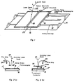
- a moving table 10 which is mounted on sliding bearings 12 secured to an optical bench 14.
- the moving table supports a photoreceptor plate 16 which may be made of any suitable material such as selenium coated onto an aluminum substrate 17.
- a sensor electrode or probe 18 is mounted over the photoreceptor plate on a supporting structure 20 secured to the optical bench 14.
- the sensor electrode or probe shown in Figure 1 is a metal strip having a longitudinal slit therein of a sufficient width to allow the passage of a laser beam 22 which is scanned across the plate through the slit in the electrode.
- the table 10 is moved on sliding bearings 12 using any suitable drive capable of advancing the photoreceptor plate step by step transversely of the laser beam scanning direction.
- an electrostatically charged photoreceptor plate which has been exposed to X-ray radiations to form a latent X-ray image of an object on the photoreceptor surface, is placed on the moving table 10 and is scanned transversely by a pulsed laser beam 22.
- the laser beam causes the photoreceptor charge for each pixel to be neutralized and a signal corresponding to its magnitude is induced in the sensor electrode 18.
- this signal is fed to a preamplifier 24 which is connected to an external measuring circuit to be disclosed later.
- a preamplifier 24 which is connected to an external measuring circuit to be disclosed later.
- the photoreceptor plate is moved longitudinally by one pixel diameter and a new transverse scan is made.
- the photoreceptor plate could be fixed and the sensor electrode movable.
- a scanning system has also been envisaged where the photoreceptor plate is continuously moving (as opposed to step by step) with respect to the sensor electrode, during the laser scanning speed has to be adjusted in concert with the laser pixel size and the width of the plate so as to produce contiguous scans across the plate.
- the image resolution is exclusively determined by the dimension of the microelectrometers, the distance between electrometers and the selenium surface and the thickness of the selenium photoreceptor, the image resolution (defined by the MTF) of the system in accordance with the present invention is almost independent of the above geometrical factors.
- the width of the probe, in the present system has to be large enough with regard to the laser beam dimension in order to achieve good capacitive coupling with the region around the area to be discharged by the laser.
- the advantage of having a relatively large probe, instead of a narrow probe of about the pixel size of the laser beam, is that the charge induced in the probe in the particular area to be discharged by the laser beam is linearly proportional to the surface charge of the selenium plate. In this situation, the horizontal component of the electric field created by a high spatial modulation of surface charge or a discharged area is averaged to zero.
- the MTF of the system is only limited by the laser spot size and the spatial sampling rate.
- the width of the sensor electrode should be more than two times the size of the laser beam. There is no advantage however in increasing the width of the sensor electrode to more than 30 mm as it would unduly increase the capaticance across the read-out device.
- the amount of charge still coupled to the conductive substrate of the selenium x-ray detector decreases as: Under the action of a pulse of light of short duration compared to the transit time of charges across the selenium thickness of the selenium plate, those neutralized charges which are free to move are only those coupled to the substrate. Thus, one would expect the signal flowing to the probe to increase at closer probe to selenium separations, due to the benefit of a better capacitive coupling.
- the substrate of the selenium layer (or the conductive probe) could be polarized to a positive or negative potential with respect to the ground.
- Cp would not be equal to Cse, but the effect of such an additional bias potential could result in a more flexible operational read-out system and one can take advantage of this benefit in order to enhance a particular parameter in image read-out.
- the probe to surface of selenium separation has to be such as to prevent self discharge of the photoreceptor charge onto the probe.
- a dielectric liquid or gas may be used to overcome field breakdown problems.
- the utilization of a dielectric fluid of the same or larger dielectric constant as selenium allows to operate at larger separations while maintaining the same optimum capacitive coupling.
- the microphonic noise due to random vibration of the probe is also reduced by a factor substantially equal to the ratio of the dielectric constant to air.
- a slit-electrode having a width of 25 mm and positioned about 1 mm for the surface of a 150 ⁇ m thick selenium plate was able to provide a sufficient signal to enable a good reproduction of the latent image on the selenium photoreceptor plate to be obtained. This image could be accurately reproduced even when the image was strongly modulated in the direction of travel of the slit-electrode.
- FIGs 4(a) and 4(b) are examples of one such improved structure, which is representative, but not restrictive as to the nature of the features which can be incorporated into the probe structure in order to improve its operation.
- the read-out probe shown in Figures 4(a) and 4(b) is a solid state device prepared by photolithographic processes on a common semi-cylindrical glass lens substrate. In order to achieve accurate alignment and positioning of the sensor electrode or probe over the photoreceptor plate, several components have been integrated to the probe.
- the read-out probe is thus composed of four components: a transparent sensor electrode designated generally by reference numral 32, an electromagnetic interference shield 34, laser alignment components 36 and capacitance structures 38 for probe micropositioning.
- a transparent sensor electrode designated generally by reference numral 32
- an electromagnetic interference shield 34 laser alignment components 36
- capacitance structures 38 for probe micropositioning.
- the number of devices integrated to the sensor electrode is not necessarily limited to these four.
- the transpatent sensor electrode 32 consists of a sputtered indium tin oxide (ITO) transparent conductive layer 40, centered with respect to a semi-cylindrical glass lens 42.
- the layer has a typical sheet resistance of 30 ohms/square and over 75% transmission for the visible spectrum.
- the width of the probe has been chosen in order to optimize the characteristic performance of the read-out system. As mentioned previously, a very narrow probe of about the pixel size of the laser would be desirable in order to reduce the microphonic noise associated with the random vibration of the probe with respect to the plate. However, a very narrow probe has a substantial limitation in terms of image resolution. A probe dimension of 1 mm in width has proven to be very satisfactory.
- the transparent sensor electrode is shielded from external electromagnetic interference by a nickel, chromium and gold multilayer shield 34 that effectively surrounds it.
- each slit 44 transversing, at a 45 degree angle, an opaque rectangle at the top of the probe.
- the centre of each slit coincides (lengthwise) with the central axis of the transparent electrode.
- a photodiode detector 46 is placed behind each of the slits 44 and the detector output is connected to an oscilloscope 47.
- the scanning laser beam is then shone along the axis of the probe.
- the probe structure is positioned in such a way that the time the laser beam is obscured from the top edge of each rectangle to the centre of each slit (T1 and T3) and the time the beam is obscured from the centre of each slit to the bottom edge of each rectangle (T2 and T4) are equal.
- T1 and T3 the time the laser beam is obscured from the centre of each slit to the bottom edge of each rectangle
- Figure 5(d) shows the inverse light intensity diagram seen on the oscilloscope when the laser beam is offset and Figure 5(e) the inverse light intensity diagram when the laser beam is centered. When all the times are equal, the laser beam is centrally traversing the transparent probe.
- capacitance structures 38 at the top and bottom of the probe. These structures consist of flat conducting pads. When the probe is positioned near the photoreceptor plate to be read out, a capacitance is formed between the pads and the plate. The capacitance of the pads with respect to selenium surface of the plates is inversely proportional to the separation of the pads from the plate.
- the capacitance of the top and bottom structures are very precisely measured using conventional bridge-type capacitane meters 48.
- the capacitance is measured directly whilst a phase signal from the bridge indicates whether or not the probe/plate separation is greater or less than a predetermined separation.
- the output of each capacitance meter is fed to a microprocessor system control 50.
- piezoelectric micropositioners 52 one at both the top and bottom of the probe structure
- a piezoelectric positioner controller 54 which is responsive to microprocessor 50, it is possible to precisely move the probe in such a way that the capacitance structures are equal.
- the probe/plate separation is constant from top to bottom of the probe. This is essential for maintaining signal uniformity along a scan.
- the selenium plate scanning system consists of a conventional optical assembly and a conventional processing and digital control.
- a galvanometer 56 is used to scan a blue laser beam (440 nm) through a F-Theta lens 58 and onto the selenium plate 16.
- the laser beam itself is generated by a laser 60 and modulated into properly timed pulses by the use of an acousto-optic modulator 62 responsive to a programmable high speed scan control 64 under the control of microprocessor 50.
- the laser itself is stabilized by an electro-optic stabilizer 66.
- the laser beam passes through a neutral density filter 68 and is deflected by mirrors 70 onto galvanometer 56.
- a translation stage controller 72 is provided for moving the photoreceptor support table 10 transversely to the scanning laser beam at the end of each scan.
- the translation stage controller is under the control of the microprocessor system control.
- the analog signal at the output of the preamplifier 24 is then processed through an analog processing unit 74 and digitized by an A/D converter 75 and stored in digital form in microprocessor 50 and can be viewed and disseminated at command using a processor and image display 76.
- the synchronization and coordination of scanning activities plus data storage may be managed by a Motorola 68000 microprocessor system and associated real-time scan logic. The details and timing of the scan process and data acquisition need not be discussed here.
- the overall results are very encouraging.
- MTF modulation transfer function
- the MTFs shown in Figure 7 are for a selenium coated plate with a selenium thickness of 150 ⁇ m, measured with a 1mm wide transparent conductive ITO electrode on glass.
- the MTF curves are for two different laser spot sizes and spatial sampling rates. For a 100 um laser spot diameter and 10 samples/mm, a resolution of 5 1p/mm has been easily attained. Also, as expected from theory, by increasing the sampling rate to 20 samples/mm and using a 50 ⁇ m laser spot size a resolution of 10 1p/mm has been achieved.
Description
- This invention relates to a system arranged to measure the charge distribution on a photoreceptor plate and, in particular, to its application to digital radiography.
- The production of X-ray images has been historically achieved by chemically developing a silver halide film, which has not been exposed to light but only to the X-ray flux from an X-ray tube which penetrates a subject. This technique is well known and need not be described in detail. The sensitivity of such methods is increased by using layers of materials which give off light when exposed to X-rays and which are included as screens in close proximity to the X-ray films inside a cassette. Although this film/screen technique increases the sensitivity, fluorescent screens of high X-ray absorption decrease the resolution of the image, which can only be enhanced within the limitations of the chemical film development methods used.
- Another method for producing X-ray images has also found widespread acceptance, particularly for mammography. This technique, termed xeroradiography, utilizes a charged selenium photoreceptor as the X-ray receptor and the image is developed by exposing the partially discharged plate, as caused by the X-ray flux falling on the plate during X-ray exposure, to a toner development method. This technique produces an image similar to that obtained with film, but with a better sensitivity and an enhanced ability to image small, low-contrast objects. This xeroradiographic technique is described in more detail in "Electrophotography" by R.M. Schaffert (Focal Press 1975).
- It has been recognized that an ability to convert the X-ray flux pattern representative of a radiograph into an equivalent electrical signal has advantages in terms of image manipulation and its optimization for diagnosis. Other benefits in terms of image storage and transmission could also be realized by such a system. The problem, up to this time, has been to retain adequate resolution and X-ray sensitivity for diagnostic and X-ray dose considerations. A number of prior developments have addressed the need for obtaining electrical signals from radiographs, but these all have shortcomings.
- Initial attempts to use digital image processing techniques for radiography involved scanning film radiographs with a light-based microdensitometer so as to obtain an electrical analog of the optical transmission distribution on the X-ray film. This method obviously has several limitations. The results can only be as good as the film system used to obtain the radiograph and there is a considerable delay between X-ray exposure and the acquisition of a digitally processed image. Commercial digitizers of this type are, however, available.
- Systems using an electrostatic imaging technique have been developed by ADAC Laboratories and Philips GmbH. Selenium plates are corona charged and exposed to the modulated X-ray beam in the same manner as current X-ray film cassettes. The latent X-ray image (caused by partial discharge of the surface charge by X-ray absorption throughout the selenium thickness) is then read out by mechanically scanning the surface of the plate with a row of microelectrometers. The electrometers are moved slowly, in relation to the plate, so as to scan the whole surface. This read-out method has shown a relatively low modulation transfer function. The electrical field perturbation due to the finite probe dimensions, the difficulties in precisely controlling the microprobe spacing over large areas, and the need to effectively decouple each microelectrometer from its neighbours are almost exclusively responsible for the limited resolution (less than 2 line-pairs/mm) of this type of system.
- A system using a laser read-out method has been disclosed in Canadian Patent No. 1,155,562 granted October 18, 1983. In this system, the surface charge distribution is read-out by scanning each pixel with a pulsed laser beam. The laser beam causes the remaining charge for each pixel to be neutralized and a signal corresponding to its magnitude is generated in an external measuring circuit. The analog current signal is then digitized and processed. The detector system consists of a transparent dielectric layer having a transparent conductive coating, which is placed in close contact (glued) with a photoconductive insulative layer (e.g., selenium). A charging regime is then used to cause a charge to be generated at the interface of the selenium which is in contact with the dielectric layer. This charged structure is exposed to X-rays and the remaining charge at the interface represents the latent X-ray image. The charge distribution is read out by monitoring the current flow to the upper conductive layer as the charge on each pixel is neutralized. A basic problem with this approach is that the dielectric sheet with the transparent conductive coating has to be of large area, covering the whole surface of the X-ray plate, and consequently when the laser discharges a single pixel, the small induced charge has to be measured in the presence of a large capacitor. This capacitor is necessarily connected across the input of the signal preamplifier, which creates an unacceptable level of noise, (unless pixels are made huge) reducing the sensitivity of the method. Also, the charging method of this invention is somewhat cumbersome and could give rise to imaging defects. Indeed, since the selenium layer is physically inaccessible, to place a charge on its surface, the structure has to be illuminated during the charging process, prior to the X-ray radiation. This charging method enhances the dark conductivity of the selenium and generates a non-uniform charge distribution on its surface.
- From the EP-A-200 300 there is already known an apparatus for the non-destructive read-out of latent electrostatic images. From the EP-A-2 102 there is known a xerographic printer/copier device which has some aspects in common with the present invention.
- It is the object of the present invention to provide a system for measuring the charge distribution on a photoreceptor plate which overcomes the difficulties associated with the X-ray imaging systems described above.
- The system, in accordance with the present invention, is recited in claim 1. The sensor electrode is of sufficient width so as to achieve good capacitive coupling with the region around the area to be discharged by the laser.
- The width of the sensor electrode preferably is more than two times the laser beam diameter.
- When the sensor electrode and the photoreceptor plate are grounded, the sensor electrode is preferably separated from the photoreceptor plate by a distance, such that the capacitance per unit area of the air gap between the sensor electrode and the photoreceptor plate is nearly equal to the capacitance per unit area of the photoreceptor plate.
- A fluid dielectric may be used instead of air in the gap between the sensor electrode and the photoreceptor plate to operate at larger separation while maintaining optimum capacitive coupling.
- The system in accordance with the present invention preferably further comprises means for maintaining constant the separation of the sensor electrode from the photoreceptor surface along the full length of the sensor electrode. Such means may include a capacitance structure at each end of the sensor, a capacitance meter associated with each capacitance structure for measuring such capacitance as an indication of the sensor electrode to photoreceptor plate separation and means responsive to such capacitance meter for adjusting the electrode/plate separation so as to maintain constant separation all along the sensor electrode.
- The system in accordance with the present invention preferably further comprises means for aligning the laser beam along the length of the sensor electrode. Such means may consist of an opaque block located on each end of the sensor electrode and having a transparent slit transversing therethrough at a 45 degree angle, the laser beam being scanned along the axis of the sensor electrode and through the slit in such opaque structure, and means for measuring the time the beam is obscured from the centre of each slit to the edges of each block as an indication of laser beam offset.
- The invention will be described by way of example with reference to a preferred embodiment illustrated in the accompanying drawings in which:
- Figure 1 shows an embodiment of a basic scanning arrangement of a photoreceptor plate by a sensor electrode;
- Figures 2(a) and 2(b) show various sensor electrode arrangements;
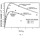
- Figure 3 shows the expected charge induced in a read-out device as a function of the sensor electrode to selenium photoreceptor plate separation.
- Figures 4(a) and 4(b) show a practical example of a transparent sensor electrode;
- Figures 5(a), 5(b), 5(c), 5(d) and 5(e) are diagrams showing a sensor electrode alignment procedure;
- Figure 6 is a diagram of a photoreceptor plate scanning system; and
- Figure 7 shows modulation transfer functions (MTFs) of selenium plates read out with a laser scanner.
- Referring to Figures 1 and 2, there is shown a moving table 10 which is mounted on sliding
bearings 12 secured to anoptical bench 14. The moving table supports aphotoreceptor plate 16 which may be made of any suitable material such as selenium coated onto analuminum substrate 17. A sensor electrode orprobe 18 is mounted over the photoreceptor plate on a supportingstructure 20 secured to theoptical bench 14. The sensor electrode or probe shown in Figure 1 is a metal strip having a longitudinal slit therein of a sufficient width to allow the passage of alaser beam 22 which is scanned across the plate through the slit in the electrode. The table 10 is moved on slidingbearings 12 using any suitable drive capable of advancing the photoreceptor plate step by step transversely of the laser beam scanning direction. - In operation, an electrostatically charged photoreceptor plate, which has been exposed to X-ray radiations to form a latent X-ray image of an object on the photoreceptor surface, is placed on the moving table 10 and is scanned transversely by a pulsed
laser beam 22. The laser beam causes the photoreceptor charge for each pixel to be neutralized and a signal corresponding to its magnitude is induced in thesensor electrode 18. - As shown in Figure 2(a), this signal is fed to a
preamplifier 24 which is connected to an external measuring circuit to be disclosed later. When a full scan across the photoreceptor plate has been completed pixel-by-pixel, the photoreceptor plate is moved longitudinally by one pixel diameter and a new transverse scan is made. It is to be understood that the photoreceptor plate could be fixed and the sensor electrode movable. A scanning system has also been envisaged where the photoreceptor plate is continuously moving (as opposed to step by step) with respect to the sensor electrode, during the laser scanning speed has to be adjusted in concert with the laser pixel size and the width of the plate so as to produce contiguous scans across the plate. - In contrast to the electrostatic read-out approach, where the image resolution is exclusively determined by the dimension of the microelectrometers, the distance between electrometers and the selenium surface and the thickness of the selenium photoreceptor, the image resolution (defined by the MTF) of the system in accordance with the present invention is almost independent of the above geometrical factors. The width of the probe, in the present system, has to be large enough with regard to the laser beam dimension in order to achieve good capacitive coupling with the region around the area to be discharged by the laser. The advantage of having a relatively large probe, instead of a narrow probe of about the pixel size of the laser beam, is that the charge induced in the probe in the particular area to be discharged by the laser beam is linearly proportional to the surface charge of the selenium plate. In this situation, the horizontal component of the electric field created by a high spatial modulation of surface charge or a discharged area is averaged to zero. Thus, in such a configuration, the MTF of the system is only limited by the laser spot size and the spatial sampling rate. The width of the sensor electrode should be more than two times the size of the laser beam. There is no advantage however in increasing the width of the sensor electrode to more than 30 mm as it would unduly increase the capaticance across the read-out device.
- The separation of the probe to the surface of selenium is an important factor for optimizing the S/N ratio of the x-ray signal. Extensive work has been done to establish optimum probe to selenium spacings. For a grounded substrate and probe, the optimum result can be understood from the following argument.
Suppose a positive charge of density + σse is initially deposited on the top surface of selenium. The negative charge density induced on the probe (σp) and on the conductive substrate of selenium (σs) will be such that:

As the probe gets closer to the surface of the selenium, the electrostatic charge induced in the probe increases as:
where Cse represents the capacitance per unit area of the selenium photoreceptor and Cp the capacitance per unit area of the air gap between the probe and the top surface of selenium.
Consequently, the amount of charge still coupled to the conductive substrate of the selenium x-ray detector decreases as:
Under the action of a pulse of light of short duration compared to the transit time of charges across the selenium thickness of the selenium plate, those neutralized charges which are free to move are only those coupled to the substrate. Thus, one would expect the signal flowing to the probe to increase at closer probe to selenium separations, due to the benefit of a better capacitive coupling. However, it has been found that the decrease in free charge able to move under the action of the laser beam, at very close separation, leads to a reduction of the signal induced in the probe, which may be expressed under the above argument as:
The optimal separation of the probe to the selenium photoreceptor, given by the condition
has been determined to be that where the capacitance formed by the air gap between the probe and selenium top surface (Cp) is equal to the capacitance of the selenium layer (Cse), that is:

Figure 3 shows the agreement between the expected theoretical and experimental measured signal induced in the probe as a function of the ratio of the air gap capacitance between the probe and the selenium plate to the selenium capacitance for two different selenium thicknesses. - In addition to the above argument, it must be understood that the substrate of the selenium layer (or the conductive probe) could be polarized to a positive or negative potential with respect to the ground. In such a case Cp would not be equal to Cse, but the effect of such an additional bias potential could result in a more flexible operational read-out system and one can take advantage of this benefit in order to enhance a particular parameter in image read-out.
- Also, it must be understood that the probe to surface of selenium separation has to be such as to prevent self discharge of the photoreceptor charge onto the probe. In the case where the optimized separation is in the breakdown region for air, it has been found that a dielectric liquid or gas may be used to overcome field breakdown problems. Also the utilization of a dielectric fluid of the same or larger dielectric constant as selenium allows to operate at larger separations while maintaining the same optimum capacitive coupling. The microphonic noise due to random vibration of the probe is also reduced by a factor substantially equal to the ratio of the dielectric constant to air.
- A slit-electrode having a width of 25 mm and positioned about 1 mm for the surface of a 150 µm thick selenium plate was able to provide a sufficient signal to enable a good reproduction of the latent image on the selenium photoreceptor plate to be obtained. This image could be accurately reproduced even when the image was strongly modulated in the direction of travel of the slit-electrode.
- A number of modifications to the basic sensor electrode arrangement shown in Figure 2(a) have been investigated. Improvements in signal have been achieved by decreasing the sensor electrode to photoreceptor surface separation, using a transparent
glass sensor electrode 26 provided with atransparent conductor 28 through which the laser beam is shone as illustrated in Figure 2(b) and reducing the width of the sensor electrode to 2 or even 0.5 mm. - More practical realizations of sensor electrode structure, however, contain various features to improve its operation. The embodiment shown in Figures 4(a) and 4(b) is an example of one such improved structure, which is representative, but not restrictive as to the nature of the features which can be incorporated into the probe structure in order to improve its operation. The read-out probe shown in Figures 4(a) and 4(b) is a solid state device prepared by photolithographic processes on a common semi-cylindrical glass lens substrate. In order to achieve accurate alignment and positioning of the sensor electrode or probe over the photoreceptor plate, several components have been integrated to the probe. The read-out probe is thus composed of four components: a transparent sensor electrode designated generally by
reference numral 32, anelectromagnetic interference shield 34,laser alignment components 36 andcapacitance structures 38 for probe micropositioning. However, the number of devices integrated to the sensor electrode is not necessarily limited to these four. - The
transpatent sensor electrode 32 consists of a sputtered indium tin oxide (ITO) transparentconductive layer 40, centered with respect to asemi-cylindrical glass lens 42. The layer has a typical sheet resistance of 30 ohms/square and over 75% transmission for the visible spectrum. - The width of the probe has been chosen in order to optimize the characteristic performance of the read-out system. As mentioned previously, a very narrow probe of about the pixel size of the laser would be desirable in order to reduce the microphonic noise associated with the random vibration of the probe with respect to the plate. However, a very narrow probe has a substantial limitation in terms of image resolution. A probe dimension of 1 mm in width has proven to be very satisfactory.
- The transparent sensor electrode is shielded from external electromagnetic interference by a nickel, chromium and
gold multilayer shield 34 that effectively surrounds it. - To assist in accurately aligning the laser read-out beam along the transparent electrode, there is a narrow
transparent slit 44 transversing, at a 45 degree angle, an opaque rectangle at the top of the probe. The centre of each slit coincides (lengthwise) with the central axis of the transparent electrode. - During the alignment procedure, as shown in Figures 5(a), 5(b) and 5(c) a
photodiode detector 46 is placed behind each of theslits 44 and the detector output is connected to anoscilloscope 47. The scanning laser beam is then shone along the axis of the probe. The probe structure is positioned in such a way that the time the laser beam is obscured from the top edge of each rectangle to the centre of each slit (T₁ and T₃) and the time the beam is obscured from the centre of each slit to the bottom edge of each rectangle (T₂ and T₄) are equal. The above measurements are all performed separately for the top and bottom structures. Figure 5(d) shows the inverse light intensity diagram seen on the oscilloscope when the laser beam is offset and Figure 5(e) the inverse light intensity diagram when the laser beam is centered. When all the times are equal, the laser beam is centrally traversing the transparent probe. - In addition to the alignment structures, there are two
capacitance structures 38 at the top and bottom of the probe. These structures consist of flat conducting pads. When the probe is positioned near the photoreceptor plate to be read out, a capacitance is formed between the pads and the plate. The capacitance of the pads with respect to selenium surface of the plates is inversely proportional to the separation of the pads from the plate. - Referring now to Figure 6, the capacitance of the top and bottom structures are very precisely measured using conventional bridge-
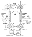
type capacitane meters 48. The capacitance is measured directly whilst a phase signal from the bridge indicates whether or not the probe/plate separation is greater or less than a predetermined separation. The output of each capacitance meter is fed to amicroprocessor system control 50. Using piezoelectric micropositioners 52 (one at both the top and bottom of the probe structure) under the control of apiezoelectric positioner controller 54 which is responsive tomicroprocessor 50, it is possible to precisely move the probe in such a way that the capacitance structures are equal. When this condition is true, the probe/plate separation is constant from top to bottom of the probe. This is essential for maintaining signal uniformity along a scan. - The selenium plate scanning system consists of a conventional optical assembly and a conventional processing and digital control. In the present setup, a
galvanometer 56 is used to scan a blue laser beam (440 nm) through a F-Theta lens 58 and onto theselenium plate 16. The laser beam itself is generated by alaser 60 and modulated into properly timed pulses by the use of an acousto-optic modulator 62 responsive to a programmable highspeed scan control 64 under the control ofmicroprocessor 50. The laser itself is stabilized by an electro-optic stabilizer 66. The laser beam passes through aneutral density filter 68 and is deflected bymirrors 70 ontogalvanometer 56. The beam passes through thesensor electrode 32 on its path from thelens 58 toselenium plate 16. The surface charge on the selenium plate induces a counter-charge on the electrode which is proportional to the charge on the plate. When the light reaches the selenium plate, the surface charge in the region of light incidence migrates to the conductive substrate of the plate, which is at a lower electric potential. This causes a simultaneous movement of charge in the electrode which is then detected by chargesensitive pre-amplifier 24. Atranslation stage controller 72 is provided for moving the photoreceptor support table 10 transversely to the scanning laser beam at the end of each scan. The translation stage controller is under the control of the microprocessor system control. - The analog signal at the output of the
preamplifier 24 is then processed through ananalog processing unit 74 and digitized by an A/D converter 75 and stored in digital form inmicroprocessor 50 and can be viewed and disseminated at command using a processor andimage display 76. The synchronization and coordination of scanning activities plus data storage, may be managed by a Motorola 68000 microprocessor system and associated real-time scan logic. The details and timing of the scan process and data acquisition need not be discussed here. - Area radiographs have been obtained with the above system and while not representative of the limiting performance of the system, they do serve to indicate the utility of the invention. The objective measurements made from such images are summarized in Table 1 and Figure 7.

- The overall results are very encouraging. For example, in the area of spatial resolution, measured by modulation transfer function (MTF) the results are excellent. The MTFs shown in Figure 7 are for a selenium coated plate with a selenium thickness of 150µm, measured with a 1mm wide transparent conductive ITO electrode on glass. The MTF curves are for two different laser spot sizes and spatial sampling rates. For a 100 um laser spot diameter and 10 samples/mm, a resolution of 5 1p/mm has been easily attained. Also, as expected from theory, by increasing the sampling rate to 20 samples/mm and using a 50 µm laser spot size a resolution of 10 1p/mm has been achieved.
- Although the invention has been disclosed with reference to preferred embodiments it is to be understood that various alternatives are envisaged within the scope of the following claims. For example, multiple probes and amplifiers combined with more elaborate laser scanning would permit sensing more than one pixel at the same time, thus permitting the read-out rate to be increased by a factor equal to the total number of amplifiers employed. In addition, the surfaces of the probe can be modified to minimize reflections of the laser beam.
Claims (9)
- A system arranged to measure the charge distribution on a photoreceptor plate (16) which has been exposed to X-ray radiation to form an image of an object thereon, said system comprising:a) a transparent sensor electrode (18) adapted to be positioned over the photoreceptor plate (16);b) means for scanning a pulsed laser beam (22) through the transparent sensor electrode to fully discharge the photoreceptor surface charge pixel-by-pixel and so induce a corresponding voltage on the sensor electrode to be read by a suitable read-out device, said sensor electrode being of sufficient width so as to achieve good capacitive coupling with the region around the area to be discharged by the laser; andc) means (10) for moving the sensor electrode or the photoreceptor plate step by step or continuously transversely of the laser scanning direction for reading out the image impressed on the photoreceptor surface.
- A system according to claim 1,
characterized in that
when said photoreceptor plate (16) and said sensor electrode (18) are grounded, the sensor electrode is separated from the photoreceptor plate by a distance such that the capacitance per unit area of the air gap between the sensor electrode and the photoreceptor plate is nearly equal to the capacitance per unit area of the photoreceptor plate. - A system according to claim 1, wherein the width of the sensor electrode (18) is more than two times the laser beam diameter.
- A system according to claim 2, wherein a fluid dielectric is used instead of air in the gap between the sensor electrode (18) and the photoreceptor plate (16).
- A system according to claim 1, further comprising means (50, 52, 54) for maintaining constant the separation of the sensor electrode from the photoreceptor plate along the full length of the sensor electrode (18).
- A system according to claim 5, wherein said maintaining constant means (50, 52, 54) comprises a capacitance structure (38) mounted at each end of the sensor electrode, a capacitance meter (48) associated with each capacitance structure for measuring such capacitance as an indication of the sensor electrode to photoreceptor plate separation, and means (52, 54) for moving said sensor electrode so as to maintain constant the separation all along the sensor electrode.
- A system according to claim 1, further comprising means (36) for aligning the laser beam along the length of the sensor electrode.
- A system according to claim 7, wherein said aligning means (36) comprises an opaque block located at each end of the sensor electrode and having a transparent slit (88) transversing therethrough at a 45 degree angle, the laser beam being scanned along the axis of the sensor electrode and through the slit in each opaque block, and means for measuring the time the beam is obscured from the centre of each slit to the edges of each block as an indication of laser beam offset.
- A system according to claim 1, wherein multiple sensor electrodes and lasers are used for permitting read-out rate of the photoreceptor plate to be increased by a factor equal to the number of sensor electrodes and lasers employed.
Applications Claiming Priority (2)
| Application Number | Priority Date | Filing Date | Title |
|---|---|---|---|
| CA000553214A CA1276320C (en) | 1987-12-01 | 1987-12-01 | System for measuring the charge distribution on a photoreceptor surface |
| CA553214 | 1987-12-01 |
Publications (2)
| Publication Number | Publication Date |
|---|---|
| EP0318807A1 EP0318807A1 (en) | 1989-06-07 |
| EP0318807B1 true EP0318807B1 (en) | 1994-02-23 |
Family
ID=4136979
Family Applications (1)
| Application Number | Title | Priority Date | Filing Date |
|---|---|---|---|
| EP88119432A Expired - Lifetime EP0318807B1 (en) | 1987-12-01 | 1988-11-22 | Systeme for measuring the charge distribution on a photoreceptor surface |
Country Status (5)
| Country | Link |
|---|---|
| US (1) | US4961209A (en) |
| EP (1) | EP0318807B1 (en) |
| CA (1) | CA1276320C (en) |
| DE (1) | DE3887968T2 (en) |
| ES (1) | ES2050141T3 (en) |
Families Citing this family (34)
| Publication number | Priority date | Publication date | Assignee | Title |
|---|---|---|---|---|
| US5168160A (en) * | 1991-06-28 | 1992-12-01 | E. I. Du Pont De Nemours And Company | Method and apparatus for acquiring an electrical signal representing a radiographic image |
| US5127038A (en) * | 1991-06-28 | 1992-06-30 | E. I. Du Pont De Nemours And Company | Method for capturing and displaying a latent radiographic image |
| US5166524A (en) * | 1991-06-28 | 1992-11-24 | E. I. Du Pont De Nemours & Company | Element, device and associated method for capturing a latent radiographic image |
| US5313066A (en) * | 1992-05-20 | 1994-05-17 | E. I. Du Pont De Nemours And Company | Electronic method and apparatus for acquiring an X-ray image |
| US5331179A (en) * | 1993-04-07 | 1994-07-19 | E. I. Du Pont De Nemours And Company | Method and apparatus for acquiring an X-ray image using a thin film transistor array |
| US5300784A (en) * | 1992-06-01 | 1994-04-05 | Xerox Corporation | Selenium alloy x-ray imaging member on transparent substrate |
| US5268569A (en) * | 1992-07-22 | 1993-12-07 | Minnesota Mining And Manufacturing Company | Imaging system having optimized electrode geometry and processing |
| US5332893A (en) * | 1992-07-22 | 1994-07-26 | Minnesota Mining And Manufacturing Company | Imaging system and device having a simplified electrode design |
| WO1994004963A1 (en) * | 1992-08-14 | 1994-03-03 | E.I. Du Pont De Nemours And Company | Element, device and associated method for capturing a latent radiographic image |
| US5319206A (en) * | 1992-12-16 | 1994-06-07 | E. I. Du Pont De Nemours And Company | Method and apparatus for acquiring an X-ray image using a solid state device |
| US5661309A (en) * | 1992-12-23 | 1997-08-26 | Sterling Diagnostic Imaging, Inc. | Electronic cassette for recording X-ray images |
| US5268950A (en) * | 1993-01-29 | 1993-12-07 | Minnesota Mining And Manufacturing Company | System and method for maintaining uniform spacing of an electrode over the surface of an x-ray plate |
| US5311033A (en) * | 1993-04-01 | 1994-05-10 | Minnesota Mining And Manufacturing Company | Layered imaging stack for minimizing interference fringes in an imaging device |
| US5381014B1 (en) * | 1993-12-29 | 1997-06-10 | Du Pont | Large area x-ray imager and method of fabrication |
| JPH09511616A (en) * | 1994-03-31 | 1997-11-18 | イメイション・コーポレイション | Imaging system with variable electrode arrangement and processing |
| US5440146A (en) * | 1994-03-31 | 1995-08-08 | Minnesota Mining And Manufacturing Company | Radiographic image reader |
| US5498880A (en) * | 1995-01-12 | 1996-03-12 | E. I. Du Pont De Nemours And Company | Image capture panel using a solid state device |
| US5686733A (en) * | 1996-03-29 | 1997-11-11 | Mcgill University | Megavoltage imaging method using a combination of a photoreceptor with a high energy photon converter and intensifier |
| FR2751095B1 (en) * | 1996-07-09 | 1998-10-30 | Thomson Csf | DEVICE FOR CONTROLLING LIGHT PULSES BY AN ACOUSTO-OPTIC PROGRAMMABLE DEVICE |
| US5994713A (en) * | 1997-06-25 | 1999-11-30 | Quantum Imaging Corp. | Filmless photon imaging apparatus |
| EP0898421A3 (en) | 1997-08-19 | 2001-12-05 | Fuji Photo Film Co., Ltd. | Electrostatic recording member, electrostatic latent image recording apparatus, and electrostatic latent image read-out apparatus |
| IL123006A (en) | 1998-01-20 | 2005-12-18 | Edge Medical Devices Ltd | X-ray imaging system |
| JP2000029612A (en) * | 1998-07-15 | 2000-01-28 | Smk Corp | Touch panel input device |
| IL126018A0 (en) | 1998-09-01 | 1999-05-09 | Edge Medical Devices Ltd | X-ray imaging system |
| US6326625B1 (en) | 1999-01-20 | 2001-12-04 | Edge Medical Devices Ltd. | X-ray imaging system |
| US6178225B1 (en) | 1999-06-04 | 2001-01-23 | Edge Medical Devices Ltd. | System and method for management of X-ray imaging facilities |
| US6717173B2 (en) * | 2000-02-08 | 2004-04-06 | Fuji Photo Film Co., Ltd. | Radio-conductive material, method of manufacturing the same, solid sensor using the same, method of manufacturing radio-conductive film, and radiation image read-out apparatus |
| US6195272B1 (en) | 2000-03-16 | 2001-02-27 | Joseph E. Pascente | Pulsed high voltage power supply radiography system having a one to one correspondence between low voltage input pulses and high voltage output pulses |
| US6590224B2 (en) | 2000-03-22 | 2003-07-08 | Fuji Photo Film Co., Ltd. | Image storage medium and method of manufacturing the same |
| JP2001264442A (en) | 2000-03-22 | 2001-09-26 | Fuji Photo Film Co Ltd | Image recording medium |
| EP1136888B1 (en) * | 2000-03-22 | 2012-01-18 | FUJIFILM Corporation | Image recording medium and method of manufacturing an image recording medium |
| JP2001281345A (en) | 2000-03-31 | 2001-10-10 | Fuji Photo Film Co Ltd | Energy ray detector and its temperature control method |
| JP4361538B2 (en) * | 2006-02-16 | 2009-11-11 | 株式会社フューチャービジョン | Static elimination method for glass substrate |
| JP6989852B2 (en) * | 2019-01-22 | 2022-02-03 | 横河電機株式会社 | Electric field sensor |
Citations (2)
| Publication number | Priority date | Publication date | Assignee | Title |
|---|---|---|---|---|
| EP0002102A1 (en) * | 1977-11-17 | 1979-05-30 | International Business Machines Corporation | Xerographic printer/copier device with converter for converting information from a latent image of an original document into electrical signals |
| EP0200300A1 (en) * | 1985-04-03 | 1986-11-05 | Emil Kamienicki | Nondestructive readout of a latent electrostatic image formed on an insulating material |
Family Cites Families (4)
| Publication number | Priority date | Publication date | Assignee | Title |
|---|---|---|---|---|
| US4085327A (en) * | 1977-01-14 | 1978-04-18 | General Electric Company | Direct charge readout electron radiography apparatus with improved signal-to-noise ratio |
| GB2048500A (en) * | 1979-05-11 | 1980-12-10 | Vacuumatic Ltd | Weighhead assemblies |
| CA1155562A (en) * | 1981-02-11 | 1983-10-18 | Ronald W. Cowart | Realtime radiation exposure monitor and control apparatus |
| DE3534768A1 (en) * | 1985-09-30 | 1987-04-02 | Philips Patentverwaltung | ARRANGEMENT FOR PRODUCING X-RAY IMAGES BY MEANS OF A PHOTOConductor |
-
1987
- 1987-12-01 CA CA000553214A patent/CA1276320C/en not_active Expired - Lifetime
-
1988
- 1988-11-22 EP EP88119432A patent/EP0318807B1/en not_active Expired - Lifetime
- 1988-11-22 ES ES88119432T patent/ES2050141T3/en not_active Expired - Lifetime
- 1988-11-22 DE DE3887968T patent/DE3887968T2/en not_active Expired - Fee Related
- 1988-11-30 US US07/278,274 patent/US4961209A/en not_active Expired - Fee Related
Patent Citations (2)
| Publication number | Priority date | Publication date | Assignee | Title |
|---|---|---|---|---|
| EP0002102A1 (en) * | 1977-11-17 | 1979-05-30 | International Business Machines Corporation | Xerographic printer/copier device with converter for converting information from a latent image of an original document into electrical signals |
| EP0200300A1 (en) * | 1985-04-03 | 1986-11-05 | Emil Kamienicki | Nondestructive readout of a latent electrostatic image formed on an insulating material |
Also Published As
| Publication number | Publication date |
|---|---|
| ES2050141T3 (en) | 1994-05-16 |
| DE3887968D1 (en) | 1994-03-31 |
| EP0318807A1 (en) | 1989-06-07 |
| DE3887968T2 (en) | 1994-10-06 |
| US4961209A (en) | 1990-10-02 |
| CA1276320C (en) | 1990-11-13 |
Similar Documents
| Publication | Publication Date | Title |
|---|---|---|
| EP0318807B1 (en) | Systeme for measuring the charge distribution on a photoreceptor surface | |
| EP0002102B1 (en) | Xerographic printer/copier device with converter for converting information from a latent image of an original document into electrical signals | |
| US6008653A (en) | Contactless system for detecting microdefects on electrostatographic members | |
| US5268569A (en) | Imaging system having optimized electrode geometry and processing | |
| JPS6252981B2 (en) | ||
| EP0991956B1 (en) | Filmless photon imaging apparatus | |
| US5168160A (en) | Method and apparatus for acquiring an electrical signal representing a radiographic image | |
| US5508507A (en) | Imaging system employing effective electrode geometry and processing | |
| JPS61292069A (en) | Nondestructive reading device and method of electrostatic latent image formed on insulating material | |
| US3752572A (en) | Apparatus for making electrographs | |
| US5127038A (en) | Method for capturing and displaying a latent radiographic image | |
| EP0573199B1 (en) | Improved selenium alloy x-ray imaging member on transparent substrate | |
| CN113169014A (en) | High resolution light valve detector for detecting X-rays | |
| US7271593B2 (en) | Contactless system and method for detecting defective points on a chargeable surface | |
| US5332893A (en) | Imaging system and device having a simplified electrode design | |
| KR20010090708A (en) | Direct radiographic imaging panel having a dielectric layer with an adjusted time constant | |
| US4636069A (en) | Method for reading deformation images on electrophotographic media | |
| US20020134944A1 (en) | Radiation image detecting system | |
| JPH02143778A (en) | Read system for electric charge latent image | |
| US3638110A (en) | Device for measuring charge on a material by converting into electrical signals the frictional forces caused by the charge | |
| US4577108A (en) | X-Ray converter foil | |
| US6756603B2 (en) | Imaging apparatus | |
| US6737667B1 (en) | Image recording medium, image retrieving method and image retrieving apparatus | |
| US3742374A (en) | Transducer device | |
| JPS59161178A (en) | Electrostatic image read-out device |
Legal Events
| Date | Code | Title | Description |
|---|---|---|---|
| PUAI | Public reference made under article 153(3) epc to a published international application that has entered the european phase |
Free format text: ORIGINAL CODE: 0009012 |
|
| AK | Designated contracting states |
Kind code of ref document: A1 Designated state(s): BE CH DE ES FR GB IT LI NL SE |
|
| 17P | Request for examination filed |
Effective date: 19891027 |
|
| 17Q | First examination report despatched |
Effective date: 19920128 |
|
| RAP1 | Party data changed (applicant data changed or rights of an application transferred) |
Owner name: NORANDA INC. |
|
| GRAA | (expected) grant |
Free format text: ORIGINAL CODE: 0009210 |
|
| AK | Designated contracting states |
Kind code of ref document: B1 Designated state(s): BE CH DE ES FR GB IT LI NL SE |
|
| PG25 | Lapsed in a contracting state [announced via postgrant information from national office to epo] |
Ref country code: SE Effective date: 19940223 Ref country code: LI Effective date: 19940223 Ref country code: CH Effective date: 19940223 |
|
| REF | Corresponds to: |
Ref document number: 3887968 Country of ref document: DE Date of ref document: 19940331 |
|
| REG | Reference to a national code |
Ref country code: ES Ref legal event code: FG2A Ref document number: 2050141 Country of ref document: ES Kind code of ref document: T3 |
|
| ITF | It: translation for a ep patent filed |
Owner name: SOCIETA' ITALIANA BREVETTI S.P.A. |
|
| REG | Reference to a national code |
Ref country code: CH Ref legal event code: PL |
|
| ET | Fr: translation filed | ||
| PLBE | No opposition filed within time limit |
Free format text: ORIGINAL CODE: 0009261 |
|
| STAA | Information on the status of an ep patent application or granted ep patent |
Free format text: STATUS: NO OPPOSITION FILED WITHIN TIME LIMIT |
|
| 26N | No opposition filed | ||
| PGFP | Annual fee paid to national office [announced via postgrant information from national office to epo] |
Ref country code: BE Payment date: 19961031 Year of fee payment: 9 |
|
| PGFP | Annual fee paid to national office [announced via postgrant information from national office to epo] |
Ref country code: ES Payment date: 19961107 Year of fee payment: 9 |
|
| PGFP | Annual fee paid to national office [announced via postgrant information from national office to epo] |
Ref country code: GB Payment date: 19961113 Year of fee payment: 9 |
|
| PGFP | Annual fee paid to national office [announced via postgrant information from national office to epo] |
Ref country code: FR Payment date: 19961126 Year of fee payment: 9 |
|
| PGFP | Annual fee paid to national office [announced via postgrant information from national office to epo] |
Ref country code: NL Payment date: 19961129 Year of fee payment: 9 |
|
| PGFP | Annual fee paid to national office [announced via postgrant information from national office to epo] |
Ref country code: DE Payment date: 19970130 Year of fee payment: 9 |
|
| PG25 | Lapsed in a contracting state [announced via postgrant information from national office to epo] |
Ref country code: GB Free format text: LAPSE BECAUSE OF NON-PAYMENT OF DUE FEES Effective date: 19971122 |
|
| PG25 | Lapsed in a contracting state [announced via postgrant information from national office to epo] |
Ref country code: ES Free format text: LAPSE BECAUSE OF NON-PAYMENT OF DUE FEES Effective date: 19971123 |
|
| PG25 | Lapsed in a contracting state [announced via postgrant information from national office to epo] |
Ref country code: FR Free format text: THE PATENT HAS BEEN ANNULLED BY A DECISION OF A NATIONAL AUTHORITY Effective date: 19971130 Ref country code: BE Free format text: LAPSE BECAUSE OF NON-PAYMENT OF DUE FEES Effective date: 19971130 |
|
| BERE | Be: lapsed |
Owner name: NORANDA INC. Effective date: 19971130 |
|
| PG25 | Lapsed in a contracting state [announced via postgrant information from national office to epo] |
Ref country code: NL Free format text: LAPSE BECAUSE OF NON-PAYMENT OF DUE FEES Effective date: 19980601 |
|
| GBPC | Gb: european patent ceased through non-payment of renewal fee |
Effective date: 19971122 |
|
| PG25 | Lapsed in a contracting state [announced via postgrant information from national office to epo] |
Ref country code: DE Free format text: LAPSE BECAUSE OF NON-PAYMENT OF DUE FEES Effective date: 19980801 |
|
| NLV4 | Nl: lapsed or anulled due to non-payment of the annual fee |
Effective date: 19980601 |
|
| REG | Reference to a national code |
Ref country code: FR Ref legal event code: ST |
|
| REG | Reference to a national code |
Ref country code: ES Ref legal event code: FD2A Effective date: 19981212 |
|
| PG25 | Lapsed in a contracting state [announced via postgrant information from national office to epo] |
Ref country code: IT Free format text: LAPSE BECAUSE OF NON-PAYMENT OF DUE FEES;WARNING: LAPSES OF ITALIAN PATENTS WITH EFFECTIVE DATE BEFORE 2007 MAY HAVE OCCURRED AT ANY TIME BEFORE 2007. THE CORRECT EFFECTIVE DATE MAY BE DIFFERENT FROM THE ONE RECORDED. Effective date: 20051122 |