EP0317063B1 - Color liquid crystal display device and method of manufacturing thereof - Google Patents
Color liquid crystal display device and method of manufacturing thereof Download PDFInfo
- Publication number
- EP0317063B1 EP0317063B1 EP88309057A EP88309057A EP0317063B1 EP 0317063 B1 EP0317063 B1 EP 0317063B1 EP 88309057 A EP88309057 A EP 88309057A EP 88309057 A EP88309057 A EP 88309057A EP 0317063 B1 EP0317063 B1 EP 0317063B1
- Authority
- EP
- European Patent Office
- Prior art keywords
- light
- colour
- shielding
- substrate
- liquid crystal
- Prior art date
- Legal status (The legal status is an assumption and is not a legal conclusion. Google has not performed a legal analysis and makes no representation as to the accuracy of the status listed.)
- Expired - Lifetime
Links
- 239000004973 liquid crystal related substance Substances 0.000 title claims description 33
- 238000004519 manufacturing process Methods 0.000 title claims description 19
- 239000000758 substrate Substances 0.000 claims description 39
- 238000004070 electrodeposition Methods 0.000 claims description 31
- 239000003086 colorant Substances 0.000 claims description 12
- 230000003287 optical effect Effects 0.000 claims description 4
- 239000000463 material Substances 0.000 claims description 3
- 239000010410 layer Substances 0.000 description 58
- 239000010408 film Substances 0.000 description 42
- 238000000034 method Methods 0.000 description 24
- 239000011521 glass Substances 0.000 description 17
- 229910052751 metal Inorganic materials 0.000 description 5
- 239000002184 metal Substances 0.000 description 5
- 239000011241 protective layer Substances 0.000 description 4
- 230000000694 effects Effects 0.000 description 3
- 238000000206 photolithography Methods 0.000 description 3
- 238000004544 sputter deposition Methods 0.000 description 3
- 229910052715 tantalum Inorganic materials 0.000 description 3
- 229910001362 Ta alloys Inorganic materials 0.000 description 2
- 230000015572 biosynthetic process Effects 0.000 description 2
- 239000011159 matrix material Substances 0.000 description 2
- 238000007639 printing Methods 0.000 description 2
- 239000010409 thin film Substances 0.000 description 2
- 239000004925 Acrylic resin Substances 0.000 description 1
- 229920000178 Acrylic resin Polymers 0.000 description 1
- 230000002411 adverse Effects 0.000 description 1
- 229910021417 amorphous silicon Inorganic materials 0.000 description 1
- 229910052804 chromium Inorganic materials 0.000 description 1
- 238000004040 coloring Methods 0.000 description 1
- 230000003247 decreasing effect Effects 0.000 description 1
- 238000000151 deposition Methods 0.000 description 1
- 230000008021 deposition Effects 0.000 description 1
- AMGQUBHHOARCQH-UHFFFAOYSA-N indium;oxotin Chemical compound [In].[Sn]=O AMGQUBHHOARCQH-UHFFFAOYSA-N 0.000 description 1
- 150000002739 metals Chemical class 0.000 description 1
- 239000000203 mixture Substances 0.000 description 1
- 229910052750 molybdenum Inorganic materials 0.000 description 1
- 238000007645 offset printing Methods 0.000 description 1
- 238000001259 photo etching Methods 0.000 description 1
- 238000007650 screen-printing Methods 0.000 description 1
- 239000004065 semiconductor Substances 0.000 description 1
- 239000000126 substance Substances 0.000 description 1
- 229920002803 thermoplastic polyurethane Polymers 0.000 description 1
- 229910052719 titanium Inorganic materials 0.000 description 1
- 238000002834 transmittance Methods 0.000 description 1
- 238000001771 vacuum deposition Methods 0.000 description 1
Images


Classifications
-
- G—PHYSICS
- G02—OPTICS
- G02F—OPTICAL DEVICES OR ARRANGEMENTS FOR THE CONTROL OF LIGHT BY MODIFICATION OF THE OPTICAL PROPERTIES OF THE MEDIA OF THE ELEMENTS INVOLVED THEREIN; NON-LINEAR OPTICS; FREQUENCY-CHANGING OF LIGHT; OPTICAL LOGIC ELEMENTS; OPTICAL ANALOGUE/DIGITAL CONVERTERS
- G02F1/00—Devices or arrangements for the control of the intensity, colour, phase, polarisation or direction of light arriving from an independent light source, e.g. switching, gating or modulating; Non-linear optics
- G02F1/01—Devices or arrangements for the control of the intensity, colour, phase, polarisation or direction of light arriving from an independent light source, e.g. switching, gating or modulating; Non-linear optics for the control of the intensity, phase, polarisation or colour
- G02F1/13—Devices or arrangements for the control of the intensity, colour, phase, polarisation or direction of light arriving from an independent light source, e.g. switching, gating or modulating; Non-linear optics for the control of the intensity, phase, polarisation or colour based on liquid crystals, e.g. single liquid crystal display cells
- G02F1/133—Constructional arrangements; Operation of liquid crystal cells; Circuit arrangements
- G02F1/1333—Constructional arrangements; Manufacturing methods
- G02F1/1335—Structural association of cells with optical devices, e.g. polarisers or reflectors
- G02F1/133509—Filters, e.g. light shielding masks
- G02F1/133512—Light shielding layers, e.g. black matrix
-
- G—PHYSICS
- G02—OPTICS
- G02F—OPTICAL DEVICES OR ARRANGEMENTS FOR THE CONTROL OF LIGHT BY MODIFICATION OF THE OPTICAL PROPERTIES OF THE MEDIA OF THE ELEMENTS INVOLVED THEREIN; NON-LINEAR OPTICS; FREQUENCY-CHANGING OF LIGHT; OPTICAL LOGIC ELEMENTS; OPTICAL ANALOGUE/DIGITAL CONVERTERS
- G02F1/00—Devices or arrangements for the control of the intensity, colour, phase, polarisation or direction of light arriving from an independent light source, e.g. switching, gating or modulating; Non-linear optics
- G02F1/01—Devices or arrangements for the control of the intensity, colour, phase, polarisation or direction of light arriving from an independent light source, e.g. switching, gating or modulating; Non-linear optics for the control of the intensity, phase, polarisation or colour
- G02F1/13—Devices or arrangements for the control of the intensity, colour, phase, polarisation or direction of light arriving from an independent light source, e.g. switching, gating or modulating; Non-linear optics for the control of the intensity, phase, polarisation or colour based on liquid crystals, e.g. single liquid crystal display cells
- G02F1/133—Constructional arrangements; Operation of liquid crystal cells; Circuit arrangements
- G02F1/1333—Constructional arrangements; Manufacturing methods
- G02F1/1335—Structural association of cells with optical devices, e.g. polarisers or reflectors
- G02F1/133509—Filters, e.g. light shielding masks
- G02F1/133514—Colour filters
Definitions
- the present invention relates to a color liquid crystal display device having a colour filter and capable of performing color display, and to a method of manufacturing thereof.
- a "pixel" of a colour display means a unitary picture element comprising means for generating respective primary colours or the equivalent.
- pixel is sometimes used in respect of means for generating just one colour.
- a light-shielding member is provided between pixels in order to prevent light leakage from the adjacent pixels, thereby obtaining high contrast.
- a light-shielding metal layer is formed on an entire surface of a substrate by vacuum deposition or sputtering method.
- the metal layer is etched to have a required shape by photoetching method.
- a protective layer is formed on the entire surface of the resultant structure. Transparent electrodes are provided on the protective layer.
- Japanese Laid-Open Gazette (Kokai) No. 60-43631 discloses a display panel in which a non-translucent member made of a thin metal film is formed between color filters.
- a dye method as an application of photolithography, a printing method as an application of offset printing or screen printing, and the like are conventionally available.
- the non-translucent layer cannot be used as an electrodeposition electrode. If a filter is to be formed by electrodeposition, a non-translucent layer, a protective layer, and a transparent electrode must be formed. Thereafter, an electrodeposition electrode must be connected to the transparent electrode, a filter must be formed by electrodeposition method, and then the electrodeposition electrode must be removed. As a result, the manufacturing process requires a large number of steps.
- a light-shielding conductive layer is formed on a substrate. Part of the light-shielding layer at a position corresponding to a pixel, for which a filter is to be formed, is removed, and simultaneously the light-shielding layer is partially removed such that portions thereof corresponding to at least pixels of different colors are electrically insulated.
- a conductive film is formed at a position corresponding to a pixel for which a filter is to be formed, and a film of a color corresponding to that of the corresponding pixel is formed on the surface of the conductive film.
- one aspect of the present invention provides a colour liquid crystal display device comprising a first and second substrate arranged mutually opposed, a layer of liquid crystal material confined between said substrates, display electrodes and address circuitry deposited on the inward looking surface of said second substrate, light-shielding layers deposited on the inward facing surface of the first substrate, transparent electrodes and colour filters of various colours, wherein the transparent electrodes are deposited on the inward facing surface of the first substrate adjacent the light-shielding layers, each said colour filter is deposited on a different one of the transparent electrodes by electrodeposition, each colour filter and corresponding transparent electrode forming a colour element, and all the colour elements are electrically connected to the light-shielding layers in such a way that each light-shielding layer is connected to a single colour element or a plurality of colour elements having the same colour.
- the light-shielding conductive film is electrically connected to the conductive film on which a color filter is to be formed. Therefore, when the light-shielding layer is used as a deposition short-circuiting electrode, a color filter and the light-shielding layer can be formed without increasing the number of manufacturing steps compared with conventional electrodeposition method.
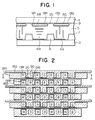
- Fig. 1 is a longitudinal sectional view of a color liquid crystal display device according to an embodiment of the present invention.
- the color liquid crystal display device shown in Fig. 1 has a glass substrate 1 on which a color filter is to be formed, and a glass substrate 2 which opposes the glass substrate 1 and on which a semiconductor drive circuit is to be arranged.
- a twisted-nematic (TN) liquid crystal 5 is sandwiched between the glass substrates 1 and 2. This is the basic structure of the device shown in Fig. 1.
- Circuits for the respective pixels are arranged in a matrix manner on the entire surface of the glass substrate 2.
- Each pixel has a transparent pixel electrode (i.e., a display electrode) 4R, 4G, or the like and an amorphous silicon thin film transistor (a-SiTFT; not shown).
- a-SiTFT amorphous silicon thin film transistor
- Ta or Al gate electrode wirings 6 having a width of about 50 ⁇ m and source electrode wirings (not shown) having a width of about 20 ⁇ m are connected to the gates and sources of the thin film transistors (TFTs) in units of rows and columns, and an orientation film 7 is formed to cover these wirings.
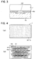
- Fig. 2 shows a pattern of transparent conductive films and light-shielding conductive layers arranged on the glass substrate 1 shown in Fig. 1.
- one display element consists of pixels of four different colors. Namely, a square red pixel, a square green pixel, a square blue pixel, and a square white (transparent) pixel are arranged at the upper left portion, the upper right portion, the lower right portion, and the lower left portion, respectively, that constitute a unit square.
- Fig. 1 is a partial sectional view taken along the line A - A′ of Fig. 2.
- Fig. 3 is a partial sectional view of a blue pixel region of the glass substrate 1.
- the liquid crystal display device shown in Figs. 1 to 3 has a structure as follows. Namely, transparent conductive films 19R, 19G, and 19B are arranged at regions of the glass substrate 1 that respectively correspond to a red display electrode 4R, a green display electrode 4G, and a blue display electrode. Light-shielding conductive layers 18R, 18G, and 18B are formed to be electrically connected to the transparent conductive films 19R, 19G, and 19B, respectively, and to extend in regions between the red, green, blue, and white pixels, respectively. Red, green, and blue filters 8R, 8G, and 8B are stacked on the transparent conductive films 19R, 19G, and 19B, respectively.
- the transparent conductive films 19R, 19G, and 19B are paired with the red display electrode 4R, the green display electrode 4G, and the blue display electrode (not shown), respectively. Each pair serves as electrodes for driving the liquid crystal.
- the light-shielding layer 18R electrically connects the plurality of red transparent conductive films 19R.
- the light-shielding layer 18G electrically connects the plurality of green transparent conductive films 19G.
- the light-shielding layer 18B electrically connects the plurality of blue transparent conductive films 19B.
- Gaps 20 between the layers 18G and 18R, between 18R and 18B, and between 18B and 18G, i.e., the regions electrically insulating these light-shielding layers are aligned with the gate electrode wirings 6 or the source electrode wirings (not shown) arranged on the glass substrate 2. Since these electrode wirings are non-translucent, they have a light-shielding effect.
- the red, green, and blue filters 8R, 8G, and 8B cover not only the transparent conductive films 19R, 19G, and 19B, but also the light-shielding layers 18R, 18G, and 18B, respectively. Since these light-shielding layers are located outside the pixel regions, no problem occurs in practice.
- a transparent conductive film 19W is formed at a region of the glass substrate 1 corresponding to a white pixel. Since no color filter is formed on the film 19W, a light-shielding layer is not connected to the film 19W.
- Each of the light-shielding layers 18R, 18G, and 18B is made of a 60 wt% Mo-40 wt% Ta alloy and has a thickness of about 1,500 ⁇ and an optical density (O.D.) of 2.0.
- the width of the gap 20 between adjacent light-shielding layers (i.e., layers 18R and 18G) of pixels for color filters of different colors is in the range of 10 to 20 ⁇ m.
- the optical density (O.D.) of the light-shielding layer 18R, 18G, or 18B is smaller than 1.5, the light-shielding layer does not often serve satisfactorily as a light-shielding layer.
- the width of the gap 20 is smaller than the range mentioned above, when the red, green, and blue filters 8R, 8G, and 8B are formed by an electrodeposition method to be described later, short circuiting easily occur; if larger, a sufficient light-shielding effect cannot be obtained with the gate electrode wirings and the source electrode wirings (not shown).
- Each of the transparent conductive films 19R, 19G, and 19B is made of, for example, ITO (indium-tin-oxide) and has a thickness of about 1,500 ⁇ .
- the light-shielding layer 18R, 18G, or 18B partially overlaps with the transparent conductive film 19R, 19G, or 19B, for about 4 to 20 ⁇ m within a portion corresponding to the corresponding display electrode4R, 4G, or the like formed on the glass substrate 2.
- a light-shielding layer and a corresponding transparent conductive film are electrically, reliably connected to each other (see Fig. 3).
- the red, green, and blue filters 8R, 8G, and 8B are formed by electrodeposition method by using the light-shielding layers 18R, 18G, and 18B as the electrodeposition electrodes, respectively, and have a thickness of about 1 to 1.5 ⁇ m.
- the thickness of the red, green, and blue filters 8R, 8G, and 8B is smaller than this range, problems tend to occur in terms of coloring; when larger, problems tend to occur in terms of cell gap control and alignment treatment.
- the light-shielding layer for electrically connecting transparent conductive films arranged in a plurality of pixel regions of the same color can be used as an electrodeposition electrode for stacking a filter member of the same color. Therefore, the light-shielding layers and the filters can be formed with a smaller number of manufacturing steps.
- gaps 20 having a width of about 10 to 20 ⁇ m exist between adjacent light-shielding layers for pixels for color filters of different colors. Light can leak from the gaps 20 to degrade the contrast.
- the gate electrode wirings 6 and the source electrode wirings (not shown) formed at portions on the glass substrate 2 corresponding to the gaps 20 light leakage is prevented and high contrast can be maintained.
- the 60 wt% Mo-40 wt% Ta layer is removed by photolithography such that it partially remains as a connecting portion for electrically connecting the same color pixels of the same row outside a position slightly (2 to 5 ⁇ m) inward a position corresponding to the pixel electrode 4R, 4G, or the like formed on the glass substrate 2, and that a gap 20 having a width of about 10 to 20 ⁇ m is present between the adjacent light-shielding layers (i.e., between layers 18R and 18G, between 18G and 18B, and between 18B and 18R) of pixels for color filters of different colors (Fig. 4(b)).
- ITO having a thickness of 1,500 ⁇ is deposited on the entire surface of the glass substrate 1 by sputtering method (Fig. 4(c)).
- green filters 8G are stacked on the transparnt conductive films 19G.
- the green filter material is also formed on the light-shielding layers 18G (not shown in Fig. 4 (d)).
- red filters 8R are stacked on the transparent conductive films 19R arranged in the red pixel regions
- blue filters 8B are stacked on the transparent conductive films 19B arranged in the blue pixel regions. Since electrodeposition is performed from the outside of the connection wire, filters are formed in the order of green, red, and blue by electrodeposition method in the structure shown in Fig. 2. Each filter has a thickness of about 1 to 1.5 ⁇ m (Fig. 4 (e)).
- the alignment film 9 is formed in accordance with the conventional manner.
- the short-circuiting of the transparent electrodes of the pixel regions which is performed in the conventional electrodeposition method can be performed during formation of the light-shielding layers. Therefore, the color filters and the light-shielding layers can be formed without increasing the number of manufacturing steps compared with the conventional electrodeposition method.
- a single display element consists of color pixels of four differnt colors.
- the single display element may consist of pixels of three different colors, e.g., red, green, and blue.
- the pixels can have a combination of mosaic patterns of red, green, and blue pixels, as shown in Fig. 5; a combination of triangular patterns of red, green, and blue pixels, as shown in Fig. 6; or a combination of square patterns of a red pixel and a blue pixel and two green pixels, as shown in Fig. 7.
- the alignment film 9 is directly coated on the color filters.
- the height difference (step difference) between the color filters and the remaining portions undesirably changes the substantial thickness of the TN liquid crystal 5.
- an acrylic resin or urethane resin can be coated to cover the nonuniform surface including the transparent conductive films 19W, thus providing a flat surface, and thereafter the alignment film 9 may be coated.
- Each transparent conductive film 19W may have an electrodeposition electrode like those of other color filters, and a white filter may be stacked on the film 19W by electrodeposition.
- an opaque (gray) filter may be used in place of a transparent filter in order to control the transmittance.
- the nonuniform surface of a case wherein a transparent or translucent filter is used can be uniformed in accordance with the above-described manner.
- the light-shielding layer is made of a 60 wt% Mo-40 wt% Ta alloy.
- the light-shielding layer can be made of other metals such as Mo, Ti, Ta, Ni, and Cr.
- a light-shielding layer for electrically connecting conductive films on which color filters are to be formed can be used as an electrodeposition short-circuiting electrode. Therefore, the light-shielding layer and the electrodeposition filters can be formed with a smaller number of manufacturing steps. As a result, a high-contrast color liquid crystal display device can be obtained in a low cost.
Landscapes
- Physics & Mathematics (AREA)
- Nonlinear Science (AREA)
- Mathematical Physics (AREA)
- Chemical & Material Sciences (AREA)
- Crystallography & Structural Chemistry (AREA)
- General Physics & Mathematics (AREA)
- Optics & Photonics (AREA)
- Liquid Crystal (AREA)
- Optical Filters (AREA)
- Devices For Indicating Variable Information By Combining Individual Elements (AREA)
Description
- The present invention relates to a color liquid crystal display device having a colour filter and capable of performing color display, and to a method of manufacturing thereof.
- Generally, in a liquid crystal display device, transparent electrodes are formed on opposing surfaces of glass substrates, which are arranged to oppose each other, to constitute a plurality of pixels, and a liquid crystal composition is sandwiched between these electrodes. It should be noted that in normal terminology, a "pixel" of a colour display means a unitary picture element comprising means for generating respective primary colours or the equivalent. However, in the following description it will be appreciated that for convenience, the term "pixel" is sometimes used in respect of means for generating just one colour.
- In such a liquid crystal display device, a light-shielding member is provided between pixels in order to prevent light leakage from the adjacent pixels, thereby obtaining high contrast.
- For example, according to a technique disclosed in Japanese Laid-Open Gazette (Kokai) No. 59-188690, a light-shielding metal layer is formed on an entire surface of a substrate by vacuum deposition or sputtering method. The metal layer is etched to have a required shape by photoetching method. A protective layer is formed on the entire surface of the resultant structure. Transparent electrodes are provided on the protective layer.
- Japanese Laid-Open Gazette (Kokai) No. 60-43631 discloses a display panel in which a non-translucent member made of a thin metal film is formed between color filters.
- As a method of forming a red (R), green (G), or blue (B) color filter at a position of a color liquid crystal display device corresponding to each pixel, a dye method as an application of photolithography, a printing method as an application of offset printing or screen printing, and the like are conventionally available.
- With the dye method, however, the decrease in throughput or manufacturing yield occurs to adversely affect the manufacturing costs. With the printing method, the precision of the device is not satisfactory.
- For these reasons, recently, a technique for forming a color filter by electrodeposition method is developed and problems of manufacturing costs and precision are being solved. More specifically, with the electrodeposition method, a large size screen can be realized, the processing time can be shortened, the heat, optical, and chemical resistances are high, and the film thickness can be freely and accurately controlled.
- However, in formation of a color filter with the electrodeposition method, when a light-shielding layer is to be formed between the pixels in order to obtain high contrast in accordance with the technique disclosed in Japanese Laid-Open Gazettes (Kokai) Nos. 59-188690, 60-43631, and the like, as described above, various problems occur.
- More specifically, in the technique disclosed in Japanese Laid-Open Gazette (Kokai) No. 59-188690, since the electrode on which a filter is to be formed and the metal non-translucent layer are electrically insulated by the protective layer, the non-translucent layer cannot be used as an electrodeposition electrode. If a filter is to be formed by electrodeposition, a non-translucent layer, a protective layer, and a transparent electrode must be formed. Thereafter, an electrodeposition electrode must be connected to the transparent electrode, a filter must be formed by electrodeposition method, and then the electrodeposition electrode must be removed. As a result, the manufacturing process requires a large number of steps.
- With the technique disclosed in Japanese Laid-Open Gazette (Kokai) No. 60-43631, since an opposing electrode, on which filters are to be formed, is provided not only on the pixel region but on the entire surface of the substrate, a filter member cannot be formed on only the pixel region by electrodeposition method.
- It is an object of the present invention to manufacture a color liquid crystal display device in which light between pixels is shielded in accordance with electrodeposition method and with a small number of manufacturing steps.
- One known liquid crystal display having different coloured pixels interspersed by light shielding layers is disclosed in EP-A-0 179 922.
- According to a method of manufacturing the color liquid crystal display device according to the present invention, a light-shielding conductive layer is formed on a substrate. Part of the light-shielding layer at a position corresponding to a pixel, for which a filter is to be formed, is removed, and simultaneously the light-shielding layer is partially removed such that portions thereof corresponding to at least pixels of different colors are electrically insulated. A conductive film is formed at a position corresponding to a pixel for which a filter is to be formed, and a film of a color corresponding to that of the corresponding pixel is formed on the surface of the conductive film.
- Thus, one aspect of the present invention provides a colour liquid crystal display device comprising a first and second substrate arranged mutually opposed, a layer of liquid crystal material confined between said substrates, display electrodes and address circuitry deposited on the inward looking surface of said second substrate, light-shielding layers deposited on the inward facing surface of the first substrate, transparent electrodes and colour filters of various colours, wherein the transparent electrodes are deposited on the inward facing surface of the first substrate adjacent the light-shielding layers, each said colour filter is deposited on a different one of the transparent electrodes by electrodeposition, each colour filter and corresponding transparent electrode forming a colour element, and all the colour elements are electrically connected to the light-shielding layers in such a way that each light-shielding layer is connected to a single colour element or a plurality of colour elements having the same colour.
- Another aspect of the present invention provides a method of manufacturing the colour liquid crystal display device according to the present invention comprises the steps of forming display electrodes and address circuitry on the inward looking surface of a second substrate, forming a light-shielding film on the inward surface of a first substrate, selectively removing parts of the light-shielding film to define a plurality of light-shielding layers and a plurality of colour element positions, forming a transparent conductive film on the first substrate including the light-shielding layers and the colour element positions and selectively removing the transparent conductive film to form a plurality of transparent electrodes corresponding to the display electrodes, and forming each colour filter of various colours on different ones of the transparent electrodes by electrodeposition using the light-shielding conductive layers as an electrodeposition short-circuiting electrode, each colour filter and corresponding transparent electrode forming a colour element, wherein all the colour elements are electrically connected to the light-shielding layers in such a way that each light-shielding layer is connected to a single colour element or a plurality of colour elements having the same colour.
- In the present invention, the light-shielding conductive film is electrically connected to the conductive film on which a color filter is to be formed. Therefore, when the light-shielding layer is used as a deposition short-circuiting electrode, a color filter and the light-shielding layer can be formed without increasing the number of manufacturing steps compared with conventional electrodeposition method.
- Embodiments of the invention will now be described by way of example only and with reference to the accompanying drawings, in which:-
- Fig. 1 is a longitudinal sectional front view of a color liquid crystal display device according to an embodiment of the present invention;
- Fig. 2 is a partial plan view showing a pattern of transparent conductive films and light-shielding layers arranged on the substrate shown in Fig. 1;
- Fig. 3 is a partial sectional view of Fig. 2;
- Fig. 4 is a partial plan view for explaining a method of manufacturing a color liquid crystal display device according to the embodiment of the present invention; and
- Figs. 5, 6, and 7 are respectively partial plan views of different color liquid crystal display devices according to other embodiments of the present invention.
- Preferred embodiments of the present invention will be described in detail with reference to the accompanying drawings.
- Fig. 1 is a longitudinal sectional view of a color liquid crystal display device according to an embodiment of the present invention.
- The color liquid crystal display device shown in Fig. 1 has a glass substrate 1 on which a color filter is to be formed, and a
glass substrate 2 which opposes the glass substrate 1 and on which a semiconductor drive circuit is to be arranged. A twisted-nematic (TN) liquid crystal 5 is sandwiched between theglass substrates 1 and 2. This is the basic structure of the device shown in Fig. 1. - Circuits for the respective pixels are arranged in a matrix manner on the entire surface of the
glass substrate 2. Each pixel has a transparent pixel electrode (i.e., a display electrode) 4R, 4G, or the like and an amorphous silicon thin film transistor (a-SiTFT; not shown). In this manner, a display surface having a plurality of matrix pixels is constituted. Ta or Al gate electrode wirings 6 having a width of about 50 µm and source electrode wirings (not shown) having a width of about 20 µm are connected to the gates and sources of the thin film transistors (TFTs) in units of rows and columns, and an orientation film 7 is formed to cover these wirings. - Fig. 2 shows a pattern of transparent conductive films and light-shielding conductive layers arranged on the glass substrate 1 shown in Fig. 1.
- In the color liquid crystal display device shown in Figs. 1 and 2, one display element consists of pixels of four different colors. Namely, a square red pixel, a square green pixel, a square blue pixel, and a square white (transparent) pixel are arranged at the upper left portion, the upper right portion, the lower right portion, and the lower left portion, respectively, that constitute a unit square. Fig. 1 is a partial sectional view taken along the line A - A′ of Fig. 2. Fig. 3 is a partial sectional view of a blue pixel region of the glass substrate 1.
- The liquid crystal display device shown in Figs. 1 to 3 has a structure as follows. Namely, transparent
conductive films red display electrode 4R, agreen display electrode 4G, and a blue display electrode.
Light-shieldingconductive layers conductive films blue filters conductive films conductive films red display electrode 4R, thegreen display electrode 4G, and the blue display electrode (not shown), respectively. Each pair serves as electrodes for driving the liquid crystal. The light-shielding layer 18R electrically connects the plurality of red transparentconductive films 19R. The light-shielding layer 18G electrically connects the plurality of green transparentconductive films 19G. The light-shielding layer 18B electrically connects the plurality of blue transparentconductive films 19B.Gaps 20 between thelayers glass substrate 2. Since these electrode wirings are non-translucent, they have a light-shielding effect. - In the liquid crystal device shown in Fig. 1, the red, green, and
blue filters conductive films shielding layers - Only a transparent
conductive film 19W is formed at a region of the glass substrate 1 corresponding to a white pixel. Since no color filter is formed on thefilm 19W, a light-shielding layer is not connected to thefilm 19W. - Each of the light-shielding
layers gap 20 between adjacent light-shielding layers (i.e., layers 18R and 18G) of pixels for color filters of different colors is in the range of 10 to 20 µm. When the optical density (O.D.) of the light-shielding layer gap 20 is smaller than the range mentioned above, when the red, green, andblue filters - Each of the transparent
conductive films - The light-
shielding layer conductive film glass substrate 2. As a result, a light-shielding layer and a corresponding transparent conductive film are electrically, reliably connected to each other (see Fig. 3). - The red, green, and
blue filters layers blue filters - In the color liquid crystal display device of this embodiment having the above-described structure, the light-shielding layer for electrically connecting transparent conductive films arranged in a plurality of pixel regions of the same color can be used as an electrodeposition electrode for stacking a filter member of the same color. Therefore, the light-shielding layers and the filters can be formed with a smaller number of manufacturing steps.
- In this embodiment, since the red, green, and
blue filters gaps 20 having a width of about 10 to 20 µm exist between adjacent light-shielding layers for pixels for color filters of different colors. Light can leak from thegaps 20 to degrade the contrast. However, because of the light-shielding effect with the gate electrode wirings 6 and the source electrode wirings (not shown) formed at portions on theglass substrate 2 corresponding to thegaps 20, light leakage is prevented and high contrast can be maintained. - A method of manufacturing the color liquid crystal display device will be described with reference to Fig. 4.
- A 60 wt% Mo-40 wt% Ta layer (O.D. = 2.0) having a thickness of 1.500 Å is deposited on the entire surface of the glass substrate 1 by sputtering method (Fig. 4(a)).
- Subsequently, the 60 wt% Mo-40 wt% Ta layer is removed by photolithography such that it partially remains as a connecting portion for electrically connecting the same color pixels of the same row outside a position slightly (2 to 5 µm) inward a position corresponding to the
pixel electrode glass substrate 2, and that agap 20 having a width of about 10 to 20 µm is present between the adjacent light-shielding layers (i.e., betweenlayers - ITO having a thickness of 1,500 Å is deposited on the entire surface of the glass substrate 1 by sputtering method (Fig. 4(c)).
- Only portions of the ITO layer corresponding to the
display electrodes glass substrate 2 are remained and the other portions are removed by photolithography (Fig. 4(d)). As a result, the transparentconductive films - Subsequently, by utilizing the light-shielding
conductive film 18G for electrically connecting the transparentconductive films 19G arranged in the green pixel regions as an electrodeposition short-circuiting electrode,green filters 8G are stacked on the transparntconductive films 19G. In this case, the green filter material is also formed on the light-shieldinglayers 18G (not shown in Fig. 4 (d)). However, since the light-shielding layer 18G is located outside the pixel regions, no problem occurs. Subsequently,red filters 8R are stacked on the transparentconductive films 19R arranged in the red pixel regions, andblue filters 8B are stacked on the transparentconductive films 19B arranged in the blue pixel regions. Since electrodeposition is performed from the outside of the connection wire, filters are formed in the order of green, red, and blue by electrodeposition method in the structure shown in Fig. 2. Each filter has a thickness of about 1 to 1.5 µm (Fig. 4 (e)). - Then, the alignment film 9 is formed in accordance with the conventional manner.
- In the manufacturing method described above, the short-circuiting of the transparent electrodes of the pixel regions which is performed in the conventional electrodeposition method can be performed during formation of the light-shielding layers. Therefore, the color filters and the light-shielding layers can be formed without increasing the number of manufacturing steps compared with the conventional electrodeposition method.
- In the above embodiment, a single display element consists of color pixels of four differnt colors. However, the single display element may consist of pixels of three different colors, e.g., red, green, and blue. In this case, the pixels can have a combination of mosaic patterns of red, green, and blue pixels, as shown in Fig. 5; a combination of triangular patterns of red, green, and blue pixels, as shown in Fig. 6; or a combination of square patterns of a red pixel and a blue pixel and two green pixels, as shown in Fig. 7.
- In the above embodiment, the alignment film 9 is directly coated on the color filters. However, as the thickness of the TN liquid crystal 5 is decreased, the height difference (step difference) between the color filters and the remaining portions undesirably changes the substantial thickness of the TN liquid crystal 5. In order to prevent this, an acrylic resin or urethane resin can be coated to cover the nonuniform surface including the transparent
conductive films 19W, thus providing a flat surface, and thereafter the alignment film 9 may be coated. - Each transparent
conductive film 19W may have an electrodeposition electrode like those of other color filters, and a white filter may be stacked on thefilm 19W by electrodeposition. In this case, an opaque (gray) filter may be used in place of a transparent filter in order to control the transmittance. The nonuniform surface of a case wherein a transparent or translucent filter is used can be uniformed in accordance with the above-described manner. - In the above embodiment, the light-shielding layer is made of a 60 wt% Mo-40 wt% Ta alloy. However, the light-shielding layer can be made of other metals such as Mo, Ti, Ta, Ni, and Cr.
- As described above, according to the color liquid crystal display device and a method of manufacturing thereof according to the present invention, a light-shielding layer for electrically connecting conductive films on which color filters are to be formed can be used as an electrodeposition short-circuiting electrode. Therefore, the light-shielding layer and the electrodeposition filters can be formed with a smaller number of manufacturing steps. As a result, a high-contrast color liquid crystal display device can be obtained in a low cost.
Claims (4)
- A colour liquid crystal display device comprising:
a first and second substrate (1, 2) arranged mutually opposed;
a layer of liquid crystal material (5) confined between said substrates (1, 2);
display electrodes (4B, 4G, 4R) and address circuitry deposited on the inward looking surface of said second substrate (2);
light-shielding layers (18B, 18G, 18R) deposited on the inward facing surface of said first substrate (1);
transparent electrodes (19B, 19G, 19R) and colour filters (8B, 8G, 8R) of various colours;
characterised in that:
said transparent electrodes (19B, 19G, 19R) are deposited on the inward facing surface of said first substrate (1) adjacent said light-shielding layers (18B, 18G, 18R); each said colour filter (8B, 8G, 8R) is deposited on a different one of said transparent electrodes (19B, 19G, 19R) by electrodeposition, each colour filter (8B, 8G, 8R) and corresponding transparent electrode (19B, 19G, 19R) forming a colour element;
all the colour elements are electrically connected to the light-shielding layers (18B, 18G, 18R) in such a way that each light-shielding layer (18B, 18G, 18R) is connected to a single colour element or a plurality of colour elements having the same colour. - A device according to claim 1, further characterised in that electrode wirings for driving the liquid crystal are formed on the second substrate (2) opposing said first substrate (1) through said liquid crystal, and an insulating region for insulating said light-shielding layers (18B, 18G, 18R) from each other is aligned with said electrode wirings.
- A device according to claim 1 or claim 2, further characterised in that said light-shielding layers (18B, 18G, 18R) have an optical density (O.D.) not less than 1.5.
- A method of manufacturing the colour liquid crystal display device comprising the steps of:
forming display electrodes (4B, 4G, 4R) and address circuitry on the inward looking surface of a second substrate (2);
forming a light-shielding film on the inward surface of a first substrate (1);
selectively removing parts of the light-shielding film to define a plurality of light-shielding layers (18B, 18G, 18R) and a plurality of colour element positions;
forming a transparent conductive film on the first substrate (1) including the light-shielding layers (18B, 18G, 18R) and the colour element positions and selectively removing the transparent conductive film to form a plurality of transparent electrodes (19B, 19G, 19R) corresponding to the display electrodes (4B, 4G, 4R); and
forming each colour filter (8B, 8G, 8R) of various colours on different ones of the transparent electrodes (19B, 19G, 19R) by electrodeposition using the light-shielding conductive layers (18B, 18G, 18R) as an electrodeposition short-circuiting electrode, each colour filter (8B, 8G, 8R) and corresponding transparent electrode (19B, 19G, 19R) forming a colour element, wherein all the colour elements are electrically connected to the light-shielding layers (18B, 18G, 18R) in such a way that each light-shielding layer (18B, 18G, 18R) is connected to a single colour element or a plurality of colour elements having the same colour.
Applications Claiming Priority (2)
| Application Number | Priority Date | Filing Date | Title |
|---|---|---|---|
| JP29167787A JPH0610702B2 (en) | 1987-11-18 | 1987-11-18 | Color liquid crystal display device and manufacturing method thereof |
| JP291677/87 | 1987-11-18 |
Publications (3)
| Publication Number | Publication Date |
|---|---|
| EP0317063A2 EP0317063A2 (en) | 1989-05-24 |
| EP0317063A3 EP0317063A3 (en) | 1990-02-07 |
| EP0317063B1 true EP0317063B1 (en) | 1994-12-28 |
Family
ID=17771994
Family Applications (1)
| Application Number | Title | Priority Date | Filing Date |
|---|---|---|---|
| EP88309057A Expired - Lifetime EP0317063B1 (en) | 1987-11-18 | 1988-09-29 | Color liquid crystal display device and method of manufacturing thereof |
Country Status (5)
| Country | Link |
|---|---|
| US (2) | US5083853A (en) |
| EP (1) | EP0317063B1 (en) |
| JP (1) | JPH0610702B2 (en) |
| CA (1) | CA1319186C (en) |
| DE (1) | DE3852617T2 (en) |
Families Citing this family (37)
| Publication number | Priority date | Publication date | Assignee | Title |
|---|---|---|---|---|
| KR960004147B1 (en) * | 1989-11-20 | 1996-03-27 | 쓰지 하루오 | Color liquid crystal display device |
| GB2245741A (en) * | 1990-06-27 | 1992-01-08 | Philips Electronic Associated | Active matrix liquid crystal devices |
| JPH04120511A (en) * | 1990-09-11 | 1992-04-21 | Sharp Corp | Liquid crystal display device |
| EP0569601B1 (en) * | 1991-11-29 | 1999-10-13 | Seiko Epson Corporation | Liquid crystal display and method of manufacturing same |
| US5459595A (en) * | 1992-02-07 | 1995-10-17 | Sharp Kabushiki Kaisha | Active matrix liquid crystal display |
| KR100294194B1 (en) * | 1993-02-05 | 2001-09-17 | 김순택 | LCD |
| JPH07114018A (en) * | 1993-10-15 | 1995-05-02 | Rohm Co Ltd | Color liquid crystal display device |
| JPH07294725A (en) * | 1994-03-01 | 1995-11-10 | Seiko Instr Inc | Method for manufacturing color filter and multicolor liquid crystal display device |
| US5642176A (en) * | 1994-11-28 | 1997-06-24 | Canon Kabushiki Kaisha | Color filter substrate and liquid crystal display device |
| US5606437A (en) * | 1995-03-31 | 1997-02-25 | Rockwell International | Direct drive split pixel structure for active matrix liquid crystal displays |
| US5936694A (en) * | 1995-04-26 | 1999-08-10 | Canon Kabushiki Kaisha | Liquid crystal device and process for producing same |
| EP0740184A3 (en) | 1995-04-28 | 1998-07-29 | Canon Kabushiki Kaisha | Liquid crystal device, process for producing same and liquid crystal apparatus |
| US5739802A (en) * | 1995-05-24 | 1998-04-14 | Rockwell International | Staged active matrix liquid crystal display with separated backplane conductors and method of using the same |
| JPH0980416A (en) * | 1995-09-13 | 1997-03-28 | Sharp Corp | Liquid crystal display device |
| EP0901032A4 (en) * | 1996-02-26 | 2000-01-12 | Kuramoto Seisakusho Co Ltd | Low reflectance film-carrying substrate |
| US20020127380A1 (en) | 1996-02-26 | 2002-09-12 | Tadakatsu Suzuki | Low-reflective thin-film substrate |
| TW384409B (en) * | 1996-06-04 | 2000-03-11 | Sharp Kk | Liquid crystal display device |
| JP2735099B2 (en) * | 1996-06-11 | 1998-04-02 | 日本電気株式会社 | Liquid crystal display |
| US5982464A (en) * | 1998-12-16 | 1999-11-09 | Technoloogy Resource International Corporation | Multi-twist color liquid crystal display |
| JP3617458B2 (en) * | 2000-02-18 | 2005-02-02 | セイコーエプソン株式会社 | Substrate for display device, liquid crystal device and electronic device |
| KR100679521B1 (en) * | 2000-02-18 | 2007-02-07 | 엘지.필립스 엘시디 주식회사 | Liquid Crystal Display Manufacturing Method |
| GB2382847A (en) | 2001-12-06 | 2003-06-11 | Alstom | Gas turbine wet compression |
| GB2382848A (en) | 2001-12-06 | 2003-06-11 | Alstom | Gas turbine wet compression |
| US7755652B2 (en) * | 2002-01-07 | 2010-07-13 | Samsung Electronics Co., Ltd. | Color flat panel display sub-pixel rendering and driver configuration for sub-pixel arrangements with split sub-pixels |
| US7417648B2 (en) | 2002-01-07 | 2008-08-26 | Samsung Electronics Co. Ltd., | Color flat panel display sub-pixel arrangements and layouts for sub-pixel rendering with split blue sub-pixels |
| US7583279B2 (en) * | 2004-04-09 | 2009-09-01 | Samsung Electronics Co., Ltd. | Subpixel layouts and arrangements for high brightness displays |
| US6888604B2 (en) * | 2002-08-14 | 2005-05-03 | Samsung Electronics Co., Ltd. | Liquid crystal display |
| DE10256193A1 (en) | 2002-12-02 | 2004-06-09 | Alstom Technology Ltd | Method for controlling the liquid injection into an inflow channel of an engine or machine |
| KR100915238B1 (en) * | 2003-03-24 | 2009-09-02 | 삼성전자주식회사 | Liquid crystal display |
| US7397455B2 (en) * | 2003-06-06 | 2008-07-08 | Samsung Electronics Co., Ltd. | Liquid crystal display backplane layouts and addressing for non-standard subpixel arrangements |
| KR100978254B1 (en) * | 2003-06-30 | 2010-08-26 | 엘지디스플레이 주식회사 | 4-pixel structure transverse electric field mode liquid crystal display device |
| JP5650918B2 (en) | 2010-03-26 | 2015-01-07 | 株式会社ジャパンディスプレイ | Image display device |
| US20130189131A1 (en) * | 2012-01-19 | 2013-07-25 | Han-Lung Huang | Water cooled motor with stainless steel cooling jacket |
| US10832616B2 (en) | 2012-03-06 | 2020-11-10 | Samsung Display Co., Ltd. | Pixel arrangement structure for organic light emitting diode display |
| KR101615332B1 (en) | 2012-03-06 | 2016-04-26 | 삼성디스플레이 주식회사 | Pixel arrangement structure for organic light emitting display device |
| JP2015146304A (en) * | 2014-02-04 | 2015-08-13 | ソニー株式会社 | Display device and electronic device |
| KR102560941B1 (en) * | 2016-09-29 | 2023-07-27 | 엘지디스플레이 주식회사 | Liquid Crystal Display Device and Liquid Crystal Display Panel |
Family Cites Families (16)
| Publication number | Priority date | Publication date | Assignee | Title |
|---|---|---|---|---|
| JPS5961818A (en) * | 1982-10-01 | 1984-04-09 | Seiko Epson Corp | liquid crystal display device |
| JPS6043631A (en) * | 1983-08-20 | 1985-03-08 | Canon Inc | Display panel |
| JPS60120321A (en) * | 1983-12-02 | 1985-06-27 | Matsushita Electric Ind Co Ltd | Color liquid crystal display device |
| JPS60172131U (en) * | 1984-04-20 | 1985-11-14 | ホシデン株式会社 | Color LCD display |
| JPS6222629A (en) * | 1985-07-23 | 1987-01-30 | 株式会社 日立メデイコ | Stereo X-ray fluoroscopy device |
| JPS6222629U (en) * | 1985-07-25 | 1987-02-10 | ||
| JPS62148926A (en) * | 1985-09-10 | 1987-07-02 | Casio Comput Co Ltd | Color liquid crystal display element |
| JPH0677120B2 (en) * | 1985-12-25 | 1994-09-28 | キヤノン株式会社 | Liquid crystal element |
| US4712874A (en) * | 1985-12-25 | 1987-12-15 | Canon Kabushiki Kaisha | Ferroelectric liquid crystal device having color filters on row or column electrodes |
| JP2511869B2 (en) * | 1986-03-18 | 1996-07-03 | シチズン時計株式会社 | Liquid crystal display |
| JP2640097B2 (en) * | 1986-03-20 | 1997-08-13 | セイコー電子工業株式会社 | Multi-color display |
| US4802743A (en) * | 1986-03-20 | 1989-02-07 | Canon Kabushiki Kaisha | Liquid crystal device having color filters wherein the color filters formed from a polyamino resin containing coloring materials |
| JPS62250416A (en) * | 1986-04-23 | 1987-10-31 | Stanley Electric Co Ltd | TFT built-in color liquid crystal display element |
| JPS62291677A (en) * | 1986-06-10 | 1987-12-18 | Toshiba Corp | Image forming device |
| FR2625827B1 (en) * | 1988-01-11 | 1993-07-16 | Commissariat Energie Atomique | COLOR DISPLAY WITH ACTIVE MATRIX WITHOUT CROSSING OF CONDUCTORS ADDRESSING LINES AND CONDUCTORS CONTROL COLUMNS |
| EP0564389A1 (en) * | 1992-04-01 | 1993-10-06 | International Business Machines Corporation | Stabilized chemically amplified positive resist composition containing glycol ether polymers |
-
1987
- 1987-11-18 JP JP29167787A patent/JPH0610702B2/en not_active Expired - Lifetime
-
1988
- 1988-09-20 US US07/246,835 patent/US5083853A/en not_active Expired - Lifetime
- 1988-09-29 EP EP88309057A patent/EP0317063B1/en not_active Expired - Lifetime
- 1988-09-29 DE DE3852617T patent/DE3852617T2/en not_active Expired - Lifetime
- 1988-10-07 CA CA000579595A patent/CA1319186C/en not_active Expired - Lifetime
-
1991
- 1991-04-30 US US07/693,621 patent/US5142392A/en not_active Expired - Lifetime
Also Published As
| Publication number | Publication date |
|---|---|
| JPH01142712A (en) | 1989-06-05 |
| US5083853A (en) | 1992-01-28 |
| CA1319186C (en) | 1993-06-15 |
| EP0317063A2 (en) | 1989-05-24 |
| EP0317063A3 (en) | 1990-02-07 |
| JPH0610702B2 (en) | 1994-02-09 |
| US5142392A (en) | 1992-08-25 |
| DE3852617T2 (en) | 1995-07-06 |
| DE3852617D1 (en) | 1995-02-09 |
Similar Documents
| Publication | Publication Date | Title |
|---|---|---|
| US5083853A (en) | Color liquid crystal display device having light-shielding conductive layers | |
| EP0179922B1 (en) | Color liquid crystal display element | |
| EP1703317B1 (en) | Liquid crystal display device | |
| US5339181A (en) | Liquid crystal display comprising a storage capacitor including the closed-ended electrode for providing a current bath for circumventing break | |
| JP2620240B2 (en) | Liquid crystal display | |
| US5285301A (en) | Liquid crystal display device having peripheral dummy lines | |
| US4644338A (en) | Dot-matrix liquid crystal display | |
| KR100244447B1 (en) | Liquid crystal display device and manufacturing method of liquid crystal display device | |
| JPH09113931A (en) | Liquid crystal display | |
| KR19980072268A (en) | Structure of Liquid Crystal Display and Manufacturing Method of Liquid Crystal Display | |
| JPH0750381B2 (en) | Color liquid crystal display | |
| WO2004011998A1 (en) | Upper substrate, liquid crystal display apparatus having the same and method of fabricating the same | |
| JPH08201853A (en) | Electrode substrate and flat display device | |
| JPS62250416A (en) | TFT built-in color liquid crystal display element | |
| US6856369B2 (en) | Electrode substrate for liquid crystal display panel, method of fabricating the electrode substrate, and liquid crystal display panel | |
| US6741305B2 (en) | Color display device | |
| JPH11237621A (en) | Liquid crystal display device and method of manufacturing liquid crystal display device | |
| JPH11258629A (en) | Manufacturing method of liquid crystal display device | |
| JPH04317027A (en) | Multicolor display device | |
| KR20000019504A (en) | Method for manufacturing lcd | |
| US20050007522A1 (en) | Liquid crystal display device | |
| KR101024642B1 (en) | LCD panel and manufacturing method | |
| JP2004053752A (en) | Liquid crystal display device | |
| JP3780529B2 (en) | Liquid crystal display device and manufacturing method thereof | |
| JP2005134904A (en) | Thin film diode display panel and manufacturing method thereof |
Legal Events
| Date | Code | Title | Description |
|---|---|---|---|
| PUAI | Public reference made under article 153(3) epc to a published international application that has entered the european phase |
Free format text: ORIGINAL CODE: 0009012 |
|
| 17P | Request for examination filed |
Effective date: 19881011 |
|
| AK | Designated contracting states |
Kind code of ref document: A2 Designated state(s): DE FR GB IT |
|
| PUAL | Search report despatched |
Free format text: ORIGINAL CODE: 0009013 |
|
| AK | Designated contracting states |
Kind code of ref document: A3 Designated state(s): DE FR GB IT |
|
| 17Q | First examination report despatched |
Effective date: 19920629 |
|
| GRAA | (expected) grant |
Free format text: ORIGINAL CODE: 0009210 |
|
| AK | Designated contracting states |
Kind code of ref document: B1 Designated state(s): DE FR GB IT |
|
| ITF | It: translation for a ep patent filed | ||
| REF | Corresponds to: |
Ref document number: 3852617 Country of ref document: DE Date of ref document: 19950209 |
|
| ET | Fr: translation filed | ||
| PLBE | No opposition filed within time limit |
Free format text: ORIGINAL CODE: 0009261 |
|
| STAA | Information on the status of an ep patent application or granted ep patent |
Free format text: STATUS: NO OPPOSITION FILED WITHIN TIME LIMIT |
|
| 26N | No opposition filed | ||
| REG | Reference to a national code |
Ref country code: GB Ref legal event code: IF02 |
|
| PGFP | Annual fee paid to national office [announced via postgrant information from national office to epo] |
Ref country code: DE Payment date: 20070927 Year of fee payment: 20 |
|
| PGFP | Annual fee paid to national office [announced via postgrant information from national office to epo] |
Ref country code: GB Payment date: 20070926 Year of fee payment: 20 |
|
| PGFP | Annual fee paid to national office [announced via postgrant information from national office to epo] |
Ref country code: IT Payment date: 20070926 Year of fee payment: 20 |
|
| PGFP | Annual fee paid to national office [announced via postgrant information from national office to epo] |
Ref country code: FR Payment date: 20070914 Year of fee payment: 20 |
|
| REG | Reference to a national code |
Ref country code: GB Ref legal event code: PE20 Expiry date: 20080928 |
|
| PG25 | Lapsed in a contracting state [announced via postgrant information from national office to epo] |
Ref country code: GB Free format text: LAPSE BECAUSE OF EXPIRATION OF PROTECTION Effective date: 20080928 |