EP0315744A1 - Photodetector for hologram-type optical head - Google Patents
Photodetector for hologram-type optical head Download PDFInfo
- Publication number
- EP0315744A1 EP0315744A1 EP88114143A EP88114143A EP0315744A1 EP 0315744 A1 EP0315744 A1 EP 0315744A1 EP 88114143 A EP88114143 A EP 88114143A EP 88114143 A EP88114143 A EP 88114143A EP 0315744 A1 EP0315744 A1 EP 0315744A1
- Authority
- EP
- European Patent Office
- Prior art keywords
- photodetector
- elements
- divided
- hologram
- piece
- Prior art date
- Legal status (The legal status is an assumption and is not a legal conclusion. Google has not performed a legal analysis and makes no representation as to the accuracy of the status listed.)
- Withdrawn
Links
- 230000003287 optical effect Effects 0.000 title claims abstract description 17
- 238000010276 construction Methods 0.000 abstract description 2
- 230000001419 dependent effect Effects 0.000 description 1
- 238000001514 detection method Methods 0.000 description 1
Images

Classifications
-
- G—PHYSICS
- G11—INFORMATION STORAGE
- G11B—INFORMATION STORAGE BASED ON RELATIVE MOVEMENT BETWEEN RECORD CARRIER AND TRANSDUCER
- G11B7/00—Recording or reproducing by optical means, e.g. recording using a thermal beam of optical radiation by modifying optical properties or the physical structure, reproducing using an optical beam at lower power by sensing optical properties; Record carriers therefor
- G11B7/12—Heads, e.g. forming of the optical beam spot or modulation of the optical beam
- G11B7/13—Optical detectors therefor
- G11B7/131—Arrangement of detectors in a multiple array
-
- G—PHYSICS
- G11—INFORMATION STORAGE
- G11B—INFORMATION STORAGE BASED ON RELATIVE MOVEMENT BETWEEN RECORD CARRIER AND TRANSDUCER
- G11B7/00—Recording or reproducing by optical means, e.g. recording using a thermal beam of optical radiation by modifying optical properties or the physical structure, reproducing using an optical beam at lower power by sensing optical properties; Record carriers therefor
- G11B7/12—Heads, e.g. forming of the optical beam spot or modulation of the optical beam
- G11B7/135—Means for guiding the beam from the source to the record carrier or from the record carrier to the detector
- G11B7/1353—Diffractive elements, e.g. holograms or gratings
-
- G—PHYSICS
- G11—INFORMATION STORAGE
- G11B—INFORMATION STORAGE BASED ON RELATIVE MOVEMENT BETWEEN RECORD CARRIER AND TRANSDUCER
- G11B7/00—Recording or reproducing by optical means, e.g. recording using a thermal beam of optical radiation by modifying optical properties or the physical structure, reproducing using an optical beam at lower power by sensing optical properties; Record carriers therefor
- G11B7/08—Disposition or mounting of heads or light sources relatively to record carriers
- G11B7/09—Disposition or mounting of heads or light sources relatively to record carriers with provision for moving the light beam or focus plane for the purpose of maintaining alignment of the light beam relative to the record carrier during transducing operation, e.g. to compensate for surface irregularities of the latter or for track following
- G11B7/0908—Disposition or mounting of heads or light sources relatively to record carriers with provision for moving the light beam or focus plane for the purpose of maintaining alignment of the light beam relative to the record carrier during transducing operation, e.g. to compensate for surface irregularities of the latter or for track following for focusing only
- G11B7/0916—Foucault or knife-edge methods
Definitions
- the present invention relates to a photodetector used for a hologram-type optical head of an optical disk apparatus.
- Fig. 3 shows an example of construction of a hologram-type optical head which performs a double-knife-edge-type focusing control by utilizing a hologram device.
- a conventional photodetector used for this kind of hologram-type optical head comprises 6-piece-divided photodiodes which include 4-piece-divided photodiodes A, B, C and D for focusing control and 2-piece-divided photodiodes E and F for tracking control which are disposed outside the 4-piece-divided photodiodes.
- a focusing error is detected by the 4-piece-divided photodiodes, that is, mere four long and narrow photodiode elements A, B, C and D.
- a laser light beam emitted from a laser diode 1 is split by a diffraction grating 2 into three light beams, and the split three light beams pass through a hologram 3, are focused by an object lens 4, and form spots on a signal surface of an optical disk 5.
- Return light beams reflected from the disk 5 return to the hologram 3 along the same paths as the incident paths.
- the hologram 3 comprises divided two areas which have respective grating patterns different from each other so that each diffracted light beam is focused on two different points on a 6-peiece-divided photodetector 6 as shown in Fig. 4.
- the wavelength of laser light beam emitted from the laser diode varies with temperature. If the wavelength of laser light beam varies, a diffraction angle by the hologram 3 is accordingly varied, whereby the spots of diffracted return light beams on the 6-piece-divided photodetector 6 are shifted in a x-direction in Fig. 4.
- the photodiode elements A, B, C, D, E and F have long and narrow shapes.
- the two spots of each return light beam on the photodetector 6 should be adjusted so as to be located on their design positions (normally, the centers of the 4-piece-divided photodiodes, that is, the positions on lines (a) shown in Fig. 4).
- design positions normally, the centers of the 4-piece-divided photodiodes, that is, the positions on lines (a) shown in Fig. 4.
- an output of each photodiode element does not vary. Therefore, it could not be performed to adjust the spot positions of the return light beams to the centers of the photodiode elements.
- an object of the invention is to provide an photodetector for the hologram-type optical head which makes it possible to adjust the spot positions of the return light beams to their design positions.
- This object is solved by the photodetector of Claim 1. Further advantageous features of the photodetector are evident from the dependent claims.
- At least one of plural photodetecting elements constituting a photodetector is divided into two small elements.
- the difference between outputs of the two small elements becomes zero when the return light spot comes to its design position and the difference takes a certain value when the return light spot is deviated from its design position. Therefore, it becomes possible to detect the deviation of the return light spots by using the outputs of the small elements.
- a photodetector of the invention is applied to a hologram-type optical head with such constitution as was described with reference to Fig. 3.
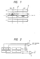
- Fig. 1 shows photodetecting elements of a photodetector according to an embodiment of the present invention.
- the photodetector comprises, as a basic constitution, a 6-piece-divided photodetector 9 consisting of 4-piece-divided photodiodes (photodetecting elements) A, B, C and D for focusing and 2-piece-divided photodiodes (photodetecting elements) E and F for tracking, and furthermore, one photodiode element A of the 4-piece-divided photodiodes is divided into two small elements A1 and A2 with the center in the x-direction as a boundary line.
- F.E. spots on photodiode elements E and F are omitted.
- the deviation of the return light spots on the photodetector 9 can be easily adjusted on the basis of the outputs of the photodiodes.
- the photodetector of the above embodiment is applied to the three-beam, hologram-type optical head, it is apparent that the present invention can be also applied to an one-beam, hologram-type optical head.
- the photodetector is not limited to the photodiodes, but, for example, phototransistors may be used as the photodetector.
Landscapes
- Physics & Mathematics (AREA)
- Optics & Photonics (AREA)
- Optical Head (AREA)
- Optical Recording Or Reproduction (AREA)
Abstract
A photodetector (9), for a hologram-type optical head comprises, as a basic construction, 6-piece-divided photodiodes (A-F). In order to prevent the photodetector from receiving the influence of wavelength variation of a laser diode (1), that is, spot deviations, one photodiode (A), is devided into two small elements (A₁,A₂) and the spot deviation is detected by utilizing the difference between outputs of the two small elements (A₁,A₂).
Description
- The present invention relates to a photodetector used for a hologram-type optical head of an optical disk apparatus.
- Fig. 3 shows an example of construction of a hologram-type optical head which performs a double-knife-edge-type focusing control by utilizing a hologram device. As shown in Fig. 4, a conventional photodetector used for this kind of hologram-type optical head comprises 6-piece-divided photodiodes which include 4-piece-divided photodiodes A, B, C and D for focusing control and 2-piece-divided photodiodes E and F for tracking control which are disposed outside the 4-piece-divided photodiodes. As shown in this figure, a focusing error is detected by the 4-piece-divided photodiodes, that is, mere four long and narrow photodiode elements A, B, C and D.
- In the hologram-type optical head shown in Fig. 3, a laser light beam emitted from a laser diode 1 is split by a diffraction grating 2 into three light beams, and the split three light beams pass through a
hologram 3, are focused by an object lens 4, and form spots on a signal surface of anoptical disk 5. Return light beams reflected from thedisk 5 return to thehologram 3 along the same paths as the incident paths. Thehologram 3 comprises divided two areas which have respective grating patterns different from each other so that each diffracted light beam is focused on two different points on a 6-peiece-divided photodetector 6 as shown in Fig. 4. In this case, a focusing error signal (F.E.), a tracking error signal (T.E.), and a reproduced RF signal (R.F.) are expressed as following respective equations:
F.E. = (A + C) - (B + D)
T.E. = E - F
R.F. = A + B + C + D
where A to F represent outputs of the corresponding photodiodes. - By the way, the wavelength of laser light beam emitted from the laser diode varies with temperature. If the wavelength of laser light beam varies, a diffraction angle by the
hologram 3 is accordingly varied, whereby the spots of diffracted return light beams on the 6-piece-divided photodetector 6 are shifted in a x-direction in Fig. 4. In order to prevent the photodetector 6 from receiving the influence of the wavelength variation of the laser diode, the photodiode elements A, B, C, D, E and F have long and narrow shapes. In this case, the two spots of each return light beam on the photodetector 6 should be adjusted so as to be located on their design positions (normally, the centers of the 4-piece-divided photodiodes, that is, the positions on lines (a) shown in Fig. 4). However, even if the spot positions of the return light beam are deviated, an output of each photodiode element does not vary. Therefore, it could not be performed to adjust the spot positions of the return light beams to the centers of the photodiode elements. - The present invention has been made to solve the foregoing problem. Accordingly, an object of the invention is to provide an photodetector for the hologram-type optical head which makes it possible to adjust the spot positions of the return light beams to their design positions. This object is solved by the photodetector of Claim 1. Further advantageous features of the photodetector are evident from the dependent claims.
- In the present invention, at least one of plural photodetecting elements constituting a photodetector is divided into two small elements.
- With the above constitution, by locating a dividing line of the two small elements at a design position of a corresponding return light spot on the photodetector, the difference between outputs of the two small elements becomes zero when the return light spot comes to its design position and the difference takes a certain value when the return light spot is deviated from its design position. Therefore, it becomes possible to detect the deviation of the return light spots by using the outputs of the small elements.
- An embodiment of the invention will be described with reference to the accompanying drawings.
- Fig. 1 illustrates a 6-piece-divided photodetector according to an embodiment of the invention;
- Fig. 2 illustrates a signal detecting circuit according to an embodiment of the invention;
- Fig. 3 illustrates a constitution of a hologram-type optical head; and
- Fig. 4 illustrates a 6-piece-divided photodetector which is employed in the optical head shown in Fig. 3.
- A photodetector of the invention is applied to a hologram-type optical head with such constitution as was described with reference to Fig. 3.
- Fig. 1 shows photodetecting elements of a photodetector according to an embodiment of the present invention. As shown in this figure, the photodetector comprises, as a basic constitution, a 6-piece-divided photodetector 9 consisting of 4-piece-divided photodiodes (photodetecting elements) A, B, C and D for focusing and 2-piece-divided photodiodes (photodetecting elements) E and F for tracking, and furthermore, one photodiode element A of the 4-piece-divided photodiodes is divided into two small elements A₁ and A₂ with the center in the x-direction as a boundary line. The difference between outputs of the small elements A₁ and A₂ is used to detect a deviation of a
return light spot 10 on the photodetector 9. That is, a subtractor 7 (which is part of a detection circuit) for obtaining the difference between the outputs of the two small elements A₁ and A₂ is provided in a focusing control circuit shown in Fig. 2, and the deviation S of thereturn light spot 10 is detected as:
S = A₁ - A₂
where A₁ and A₂ represent outputs of the corresponding small elements. - The outputs of the two elements A₁ and A₂ branch off to be added to each other and then provided to a
subtractor 8. Therefore, a focusing error signal (F.E.) is expressed as:
F.E. = ((A₁ + A₂) + C) - (B + D).
In Fig. 1, spots on photodiode elements E and F are omitted. - With the above constitution, in adjusting the spots of the return light beams reflected from a signal surface of an optical disk to their design positions on the photodetector 9, in this case, to the centers in the x-direction of the photodiode elements A, B, C and D (the positions on line (a) in Fig. 1), when the two spots of the return light beam are deviated from the centers in the x-direction of the photodiode elements A, B, C and D, the
spot 10 is deviated from the boundary line between the two small elements A₁ and A₂ and the difference occurs in the outputs of the two small elements. Therefore, the completion of such adjustment of the return light beam that the outputs of the two small elements A₁ and A₂ are made to be zero (that is, S = A₁ - A₂ = 0) means that the center of thereturn light spot 10 has been made coincident with the boundary line between the two small elements A₁ and A₂. This also means that the return light spots are made coincident with the centers (design positions) in the x-direction of the elements A, B, C and D. In the above-described manner, the deviation of the return light spots on the photodetector 9 can be easily adjusted on the basis of the outputs of the photodiodes. - Although the photodetector of the above embodiment is applied to the three-beam, hologram-type optical head, it is apparent that the present invention can be also applied to an one-beam, hologram-type optical head. Moreover, the photodetector is not limited to the photodiodes, but, for example, phototransistors may be used as the photodetector.
Claims (3)
1. A photodetector (9) for a hologram-type optical head, comprising:
a plurality of photodetecting elements (A-F) for detecting return light beams reflected from an optical disk (5) and then diffracted by a hologram (3) at least one of said photodetecting element (A) being divided into two small elements (A₁,A₂); and
a signal detecting circuit (7,8) for detecting a difference between outputs of said two small elements (A₁,A₂) as a spot deviation signal.
2. A photodetector as claimed in claim 1, wherein said plurality of photodetecting elements comprises 4-piece-divided photodetecting elements (A,B,C,D), for detecting a focusing error and 2-piece-divided photodetecting elements (E,F), for detecting a tracking error which are disposed outside said 4-piece-divided photodetecting elements (A,B,C,D) and one of said 4-piece-divided photodetecting elements (A,B,C,D) is divided into said two small elements (A₁A₂).
3. A photodetector as claimed in claim 1 or 2, wherein said outputs of said small elements (A₁,A₂) branch off to be added to each other to form a focusing error signal.
Applications Claiming Priority (2)
| Application Number | Priority Date | Filing Date | Title |
|---|---|---|---|
| JP62285062A JPH0827961B2 (en) | 1987-11-11 | 1987-11-11 | Holographic optical head photodetector |
| JP285062/87 | 1987-11-11 |
Publications (1)
| Publication Number | Publication Date |
|---|---|
| EP0315744A1 true EP0315744A1 (en) | 1989-05-17 |
Family
ID=17686666
Family Applications (1)
| Application Number | Title | Priority Date | Filing Date |
|---|---|---|---|
| EP88114143A Withdrawn EP0315744A1 (en) | 1987-11-11 | 1988-08-30 | Photodetector for hologram-type optical head |
Country Status (3)
| Country | Link |
|---|---|
| US (1) | US5001334A (en) |
| EP (1) | EP0315744A1 (en) |
| JP (1) | JPH0827961B2 (en) |
Cited By (3)
| Publication number | Priority date | Publication date | Assignee | Title |
|---|---|---|---|---|
| EP0457573A1 (en) * | 1990-05-15 | 1991-11-21 | Sharp Kabushiki Kaisha | Optical head |
| US5283772A (en) * | 1990-05-15 | 1994-02-01 | Sharp Kabushiki Kaisha | Optical head |
| US5428595A (en) * | 1992-01-28 | 1995-06-27 | Sharp Kabushiki Kaisha | Optical information recording and reproducing device |
Families Citing this family (4)
| Publication number | Priority date | Publication date | Assignee | Title |
|---|---|---|---|---|
| DE68913681T2 (en) * | 1988-12-20 | 1994-06-16 | Nippon Electric Co | Optical head for optimal detection of a focus error. |
| JPH077511B2 (en) * | 1989-02-21 | 1995-01-30 | パイオニア株式会社 | Device for detecting reading position deviation in disc player |
| JPH05210858A (en) * | 1991-10-29 | 1993-08-20 | Internatl Business Mach Corp <Ibm> | Optical type data storage system having aberration compensation for reducing servo-crosstalk |
| US5777352A (en) * | 1996-09-19 | 1998-07-07 | Eastman Kodak Company | Photodetector structure |
Citations (2)
| Publication number | Priority date | Publication date | Assignee | Title |
|---|---|---|---|---|
| EP0238055A2 (en) * | 1986-03-19 | 1987-09-23 | Sanyo Electric Co., Ltd. | Optical recording apparatus |
| EP0273356A2 (en) * | 1986-12-25 | 1988-07-06 | Nec Corporation | An optical head |
Family Cites Families (6)
| Publication number | Priority date | Publication date | Assignee | Title |
|---|---|---|---|---|
| NL160138C (en) * | 1972-05-11 | 1979-09-17 | Philips Nv | DEVICE FOR READING A FLAT REGISTRATION CARRIER. |
| JPS59147306A (en) * | 1983-02-10 | 1984-08-23 | Sony Corp | Focus error detection device |
| JPS6070923U (en) * | 1983-10-19 | 1985-05-20 | パイオニア株式会社 | Focus error detection device |
| JPS6095733A (en) * | 1983-10-31 | 1985-05-29 | Hitachi Ltd | Optical signal processor |
| JPS60185230A (en) * | 1984-03-02 | 1985-09-20 | Pioneer Electronic Corp | Focal error detector |
| JPH0746439B2 (en) * | 1985-04-09 | 1995-05-17 | キヤノン株式会社 | Optical head device |
-
1987
- 1987-11-11 JP JP62285062A patent/JPH0827961B2/en not_active Expired - Lifetime
-
1988
- 1988-08-30 EP EP88114143A patent/EP0315744A1/en not_active Withdrawn
- 1988-08-30 US US07/238,138 patent/US5001334A/en not_active Expired - Fee Related
Patent Citations (2)
| Publication number | Priority date | Publication date | Assignee | Title |
|---|---|---|---|---|
| EP0238055A2 (en) * | 1986-03-19 | 1987-09-23 | Sanyo Electric Co., Ltd. | Optical recording apparatus |
| EP0273356A2 (en) * | 1986-12-25 | 1988-07-06 | Nec Corporation | An optical head |
Cited By (3)
| Publication number | Priority date | Publication date | Assignee | Title |
|---|---|---|---|---|
| EP0457573A1 (en) * | 1990-05-15 | 1991-11-21 | Sharp Kabushiki Kaisha | Optical head |
| US5283772A (en) * | 1990-05-15 | 1994-02-01 | Sharp Kabushiki Kaisha | Optical head |
| US5428595A (en) * | 1992-01-28 | 1995-06-27 | Sharp Kabushiki Kaisha | Optical information recording and reproducing device |
Also Published As
| Publication number | Publication date |
|---|---|
| JPH0827961B2 (en) | 1996-03-21 |
| US5001334A (en) | 1991-03-19 |
| JPH01125739A (en) | 1989-05-18 |
Similar Documents
| Publication | Publication Date | Title |
|---|---|---|
| US5016954A (en) | Optical pickup and hologram therefor | |
| EP0219908B1 (en) | Apparatus for optically scanning an information plane | |
| US4011400A (en) | Apparatus for reading an optically readable reflecting information structure | |
| KR880001707B1 (en) | Photoelectric Focusing Error Detection Device | |
| EP0426879B1 (en) | Optical recording and/or reproducing apparatus | |
| EP0365368B1 (en) | An optical pickup device | |
| EP0075676B1 (en) | Optical track position detecting apparatus and optical disc apparatus using the same | |
| US5608695A (en) | Optical pick-up apparatus with tracking error detection by detection of amount of light in fan field | |
| KR910001671A (en) | Optical pickup | |
| EP0369510A1 (en) | Apparatus for optically scanning a radiation-reflecting information plane | |
| US5231621A (en) | Focus detector which serves to split off a portion of a detected light beam only when the detected light beam is not refocused at an expected refocus point | |
| EP0315744A1 (en) | Photodetector for hologram-type optical head | |
| EP0612064B1 (en) | An optical pickup apparatus | |
| US5029261A (en) | Apparatus for detecting position of light beam on object surface by comparing detection beams split near focal point | |
| US6512732B1 (en) | Device for optically scanning information tracks on a plane using two subbeams | |
| EP0831470B1 (en) | Recording or replay device for recording on or replaying from an optical recording medium | |
| EP0273422A2 (en) | A method and apparatus for detecting track and focus errors in an optical head | |
| US6466526B1 (en) | Apparatus for recording and replaying information on optical information record medium and optical pickup | |
| JP2594445B2 (en) | Hologram optical head | |
| KR0176600B1 (en) | Control and discrimination signal detection device and tracking error signal detection method for multi beam optical disc player | |
| JP2552660B2 (en) | Focus error detector | |
| US4270045A (en) | Apparatus for reading an optical radiation-reflecting information carrier for controlling focus | |
| EP0628955B1 (en) | Optical head | |
| EP0468116B1 (en) | Signal detector | |
| JP2596993B2 (en) | Information reading method for optical disk |
Legal Events
| Date | Code | Title | Description |
|---|---|---|---|
| PUAI | Public reference made under article 153(3) epc to a published international application that has entered the european phase |
Free format text: ORIGINAL CODE: 0009012 |
|
| AK | Designated contracting states |
Kind code of ref document: A1 Designated state(s): DE FR GB |
|
| 17P | Request for examination filed |
Effective date: 19891117 |
|
| 17Q | First examination report despatched |
Effective date: 19910822 |
|
| STAA | Information on the status of an ep patent application or granted ep patent |
Free format text: STATUS: THE APPLICATION IS DEEMED TO BE WITHDRAWN |
|
| 18D | Application deemed to be withdrawn |
Effective date: 19920303 |