EP0308946B1 - Chemical vapor deposition apparatus for obtaining high quality epitaxial layer with uniform film thickness - Google Patents
Chemical vapor deposition apparatus for obtaining high quality epitaxial layer with uniform film thickness Download PDFInfo
- Publication number
- EP0308946B1 EP0308946B1 EP88115622A EP88115622A EP0308946B1 EP 0308946 B1 EP0308946 B1 EP 0308946B1 EP 88115622 A EP88115622 A EP 88115622A EP 88115622 A EP88115622 A EP 88115622A EP 0308946 B1 EP0308946 B1 EP 0308946B1
- Authority
- EP
- European Patent Office
- Prior art keywords
- gas
- wafer
- tube
- nozzle tube
- emission
- Prior art date
- Legal status (The legal status is an assumption and is not a legal conclusion. Google has not performed a legal analysis and makes no representation as to the accuracy of the status listed.)
- Expired - Lifetime
Links
- 238000005229 chemical vapour deposition Methods 0.000 title claims description 21
- 239000000758 substrate Substances 0.000 claims description 22
- 238000010438 heat treatment Methods 0.000 claims description 6
- 235000012431 wafers Nutrition 0.000 description 161
- 239000007789 gas Substances 0.000 description 34
- 229910003818 SiH2Cl2 Inorganic materials 0.000 description 16
- 239000012159 carrier gas Substances 0.000 description 14
- 238000010586 diagram Methods 0.000 description 10
- 238000000034 method Methods 0.000 description 7
- NJPPVKZQTLUDBO-UHFFFAOYSA-N novaluron Chemical compound C1=C(Cl)C(OC(F)(F)C(OC(F)(F)F)F)=CC=C1NC(=O)NC(=O)C1=C(F)C=CC=C1F NJPPVKZQTLUDBO-UHFFFAOYSA-N 0.000 description 4
- 229910003822 SiHCl3 Inorganic materials 0.000 description 3
- 230000007423 decrease Effects 0.000 description 2
- 238000009434 installation Methods 0.000 description 2
- 238000004519 manufacturing process Methods 0.000 description 2
- 239000000203 mixture Substances 0.000 description 2
- 230000002093 peripheral effect Effects 0.000 description 2
- UFHFLCQGNIYNRP-UHFFFAOYSA-N Hydrogen Chemical compound [H][H] UFHFLCQGNIYNRP-UHFFFAOYSA-N 0.000 description 1
- XUIMIQQOPSSXEZ-UHFFFAOYSA-N Silicon Chemical compound [Si] XUIMIQQOPSSXEZ-UHFFFAOYSA-N 0.000 description 1
- 229910021417 amorphous silicon Inorganic materials 0.000 description 1
- 239000013078 crystal Substances 0.000 description 1
- 230000001419 dependent effect Effects 0.000 description 1
- 230000000694 effects Effects 0.000 description 1
- 239000001257 hydrogen Substances 0.000 description 1
- 229910052739 hydrogen Inorganic materials 0.000 description 1
- 229910021420 polycrystalline silicon Inorganic materials 0.000 description 1
- 229920005591 polysilicon Polymers 0.000 description 1
- 239000000523 sample Substances 0.000 description 1
- 239000004065 semiconductor Substances 0.000 description 1
- 229910052710 silicon Inorganic materials 0.000 description 1
- 239000010703 silicon Substances 0.000 description 1
Images






Classifications
-
- C—CHEMISTRY; METALLURGY
- C30—CRYSTAL GROWTH
- C30B—SINGLE-CRYSTAL GROWTH; UNIDIRECTIONAL SOLIDIFICATION OF EUTECTIC MATERIAL OR UNIDIRECTIONAL DEMIXING OF EUTECTOID MATERIAL; REFINING BY ZONE-MELTING OF MATERIAL; PRODUCTION OF A HOMOGENEOUS POLYCRYSTALLINE MATERIAL WITH DEFINED STRUCTURE; SINGLE CRYSTALS OR HOMOGENEOUS POLYCRYSTALLINE MATERIAL WITH DEFINED STRUCTURE; AFTER-TREATMENT OF SINGLE CRYSTALS OR A HOMOGENEOUS POLYCRYSTALLINE MATERIAL WITH DEFINED STRUCTURE; APPARATUS THEREFOR
- C30B25/00—Single-crystal growth by chemical reaction of reactive gases, e.g. chemical vapour-deposition growth
- C30B25/02—Epitaxial-layer growth
- C30B25/12—Substrate holders or susceptors
-
- C—CHEMISTRY; METALLURGY
- C30—CRYSTAL GROWTH
- C30B—SINGLE-CRYSTAL GROWTH; UNIDIRECTIONAL SOLIDIFICATION OF EUTECTIC MATERIAL OR UNIDIRECTIONAL DEMIXING OF EUTECTOID MATERIAL; REFINING BY ZONE-MELTING OF MATERIAL; PRODUCTION OF A HOMOGENEOUS POLYCRYSTALLINE MATERIAL WITH DEFINED STRUCTURE; SINGLE CRYSTALS OR HOMOGENEOUS POLYCRYSTALLINE MATERIAL WITH DEFINED STRUCTURE; AFTER-TREATMENT OF SINGLE CRYSTALS OR A HOMOGENEOUS POLYCRYSTALLINE MATERIAL WITH DEFINED STRUCTURE; APPARATUS THEREFOR
- C30B25/00—Single-crystal growth by chemical reaction of reactive gases, e.g. chemical vapour-deposition growth
- C30B25/02—Epitaxial-layer growth
- C30B25/14—Feed and outlet means for the gases; Modifying the flow of the reactive gases
-
- Y—GENERAL TAGGING OF NEW TECHNOLOGICAL DEVELOPMENTS; GENERAL TAGGING OF CROSS-SECTIONAL TECHNOLOGIES SPANNING OVER SEVERAL SECTIONS OF THE IPC; TECHNICAL SUBJECTS COVERED BY FORMER USPC CROSS-REFERENCE ART COLLECTIONS [XRACs] AND DIGESTS
- Y10—TECHNICAL SUBJECTS COVERED BY FORMER USPC
- Y10S—TECHNICAL SUBJECTS COVERED BY FORMER USPC CROSS-REFERENCE ART COLLECTIONS [XRACs] AND DIGESTS
- Y10S148/00—Metal treatment
- Y10S148/006—Apparatus
-
- Y—GENERAL TAGGING OF NEW TECHNOLOGICAL DEVELOPMENTS; GENERAL TAGGING OF CROSS-SECTIONAL TECHNOLOGIES SPANNING OVER SEVERAL SECTIONS OF THE IPC; TECHNICAL SUBJECTS COVERED BY FORMER USPC CROSS-REFERENCE ART COLLECTIONS [XRACs] AND DIGESTS
- Y10—TECHNICAL SUBJECTS COVERED BY FORMER USPC
- Y10S—TECHNICAL SUBJECTS COVERED BY FORMER USPC CROSS-REFERENCE ART COLLECTIONS [XRACs] AND DIGESTS
- Y10S438/00—Semiconductor device manufacturing: process
- Y10S438/935—Gas flow control
Definitions
- the present invention relates to a chemical vapor deposition (CVD) apparatus and, more particularly, to a CVD apparatus for silicon epitaxial growth.
- CVD chemical vapor deposition
- Si epitaxial wafers Si wafers with epitaxial films
- diameters of the Si wafers have become as large as 125 mm to 150 mm(5 to 6 inches) to reduce the process costs.
- a wafer-processing capacity of the conventional CVD apparatus was small, a large number of Si wafers of large diameters could not be treated simultaneously, resulting in the expensive cost for manufacturing epitaxial wafers.
- the uniform film thickness and the uniform crystal quality could not be obtained over the entire Si wafer of large diameter.
- a CVD apparatus For improving a growth of the uniform epitaxial layer on the Si wafer of large diameter, a CVD apparatus was proposed in Japanese Laid open patent 62-173712.
- Si wafers having diameters of 150 mm (6 inches) were vertically stacked in a wafer holder.
- the wafer holder was rotated so as to supply the starting gases on the Si wafers through holes of a gas-supply nozzle tube, the direction of the holes being deviated from the rotation center of each Si wafer.
- the number of the gas-supply nozzle tube was only one.
- the flow of the starting gases over the Si wafer was still nonuniform, especially over the Si wafer of a large diameter. Therefore, the obtained uniformity of the epitaxial layer does not have a level required for using for large-scale integrated circuits.
- a third gas-supply nozzle tube may be added to the first and second gas-supply nozzle tubes, the two gas-emitting-axes of the gas-emission holes of the first and third gas-supply nozzle tubes and the two gas-emitting-axes of the second and third gas-supply nozzle tubes respectively intersecting each other over the Si wafer and these intersections being also deviated from the center of each Si wafer.
- the gas-emission holes may be formed in the plural columns, each of the columns having the gas-emission holes in a vertical direction.
- the gas-supply nozzle tube favorably has gas-inlet portions at its both ends.
- the gas-supply nozzle tube also favorably has gas inlet portion at its center.
- an outer reaction tube 11 and an inner reaction tube 7 having an inner diameter of 240 mm are installed on a pedestal 14.
- a wafer holder 6 is installed in the inner reaction tube 7.
- 30 Si wafers 5 having a diameter of 150 mm (6 inches) are piled in a vertical direction with a space of 10 mm.
- Gas-supply nozzle tubes 8 and 9 are installed vertically near the wafer holder 6. Starting-gases are introduced through the nozzle tubes 8 and 9 over the Si wafers 5 and exhausted through holes 10 formed in the wall of the inner reaction tube 7 and a vent 12 formed in the outer reaction tube 11.
- the Si wafers 5 are heated by a resistance-heating furnace 13.
- a typical form of the nozzle tube 9 is shown and is formed of a main nozzle tube 91 having an inner diameter of 20 mm and having gas-emission holes 94, 95 and 96 of an inner diameter of 1 mm, a branch nozzle tube 92 of an inner diameter of 10 mm, and a gas-inlet tube 93 of an inner diameter of 10 mm connected to both the bottom ends of the main and branch nozzle tubes 91 and 92.
- the top end and the bottom end of the branch nozzle tube 92 are respectively connected to the top end and the bottom end of the main nozzle tube 91.
- the interval of the gas-emission holes 94, 95 and 96 in the vertical direction is 10 mm, the holes 94, 95 and 96 being respectively positioned between adjacent Si wafers 5 to introduce the starting-gases over each Si wafer 5.
- the nozzle tube 8 has a main nozzle tube 81 and a branch nozzle tube 82 and has a similar structure to the nozzle tube 9 but has only one gas-supply column in which many gas-emission holes 83 are formed in the vertical direction.
- the space L between the edge of the Si wafer 5 and the centers of the nozzle tube 81 and 91 is 35 mm.
- the line connecting the center of the Si wafer 5 and the center of the main nozzle tube 81 intersects the line connecting the center of the Si wafer 5 and the center of the main nozzle tube 91 with an angle of 30°.
- a gas-emitting-axis 83a of a gas blown from the gas-emission hole 83 (hereinafter, the line connecting the center of a main nozzle tube and the center of a gas-emission hole formed in the wall of the main nozzle tube is referred to as a gas-emitting-axis of its gas-emission hole; therefore, in this case, this gas-emitting-axis 83a of the gas-emission hole 83 is identical with the line connecting the center of the main nozzle 81 and the center of the gas-emission hole 83) is deviated from the center of Si wafer 5 toward its left-hand side.
- the angle of this gas-emitting-axis 83a formed with the line connecting both the centers of the Si wafer 5 and the main nozzle tube 81 is designed at 15°.
- a gas-emitting-axis 94a of the gas-emission hole 94 passes just above the center of the Si wafer 5.
- a gas-emitting-axis 95a of the gas-emission hole 95 is deviated from the center of the Si wafer 5 toward its right-hand side.
- the angle between this gas-emitting-axis 95a and the line connecting both the centers of the Si wafer 5 and the main nozzle 91 is designed at 15°.
- a gas-emitting-axis 96a of the gas-emission hole 96 is deviated from the center of the Si wafer 5 toward its right-hand side.
- the angle between this gas-emitting-axis 96a and the line connecting both the centers of the Si wafer 5 and the main nozzle 91 is designed at 30°.
- a mixture of Ar, SiH2Cl2, HCl and PH3 is introduced into the inner reaction tube 7 through the nozzle tube 9, together with H2 introduced through the nozzle tube 8.
- Flow rates of Ar, SiH2Cl2, HCl and H2 are respectively controlled at 20 l/min, 400 cc/min, 300 cc/min and 20 l/min.
- PH3 of 50 ppm in Ar is 300 times diluted by H2 and thus diluted gas is introduced at a flow rate of 50 cc/min.
- Epitaxial growth is carried out at 1,000°C, keeping the total pressure in the inner reaction tube 7 at ca. 1,3 kPa (10 Torr).
- the film thickness of the epitaxial layer is measured by an IR interference method, the resistivity of the epitaxial layer being measured by a four-point probe technique.
- the epitaxial layer obtained in accordance with the present embodiment shows an excellent uniformity. That is, both the uniformity on a wafer of the growth rate of the epitaxial layer and the uniformity on the wafer of the resistivity of the epitaxial layer were within ⁇ 5%.
- uniformity of the growth rate of the epitaxial layer grown in accordance with the present embodiment (see curve 41) is superior to that of the epitaxial layer grown by a gas-supply nozzle tube 45 of one gas-emission holes 46 shown in Fig. 4(c).
- a curve 42 was obtained by setting the gas-emitting-axis 46a of the gas-emission hole 46 passing just above the center of the Si wafer 5, and a curve 43 was obtained by setting the gas-emitting-axis 46a of the gas-emission hole 46 so as to deviate from the center of the Si wafer 5 toward its right-hand side, the angle between this gas-emitting-axis 46a and the line connecting both the centers of the Si wafer 5 and the nozzle tube 45 being 15°, the gas-emitting-axis 83a being deviated from the center of the Si wafer 5 toward its left-hand side, the angle of the gas-emitting-axis 83a and the line connecting both the centers of the Si wafer 5 and the nozzle tube 81 being 15°.
- H2 is introduced by the nozzle tube 81 at a flow rate of 20 l/min together with Ar, SiH2Cl2, HCl and PH3 introduced through the nozzle tube 45 at flow rates of 12 l/min, 400 cc/min, 300 cc/min and 50 cc/min, respectively.
- wafer-to-wafer uniformity of the growth rate of the epitaxial layer grown in accordance with the present embodiment is excellent and superior to that of the epitaxial layer (see curve 52) grown by using the gas-supply nozzle tube 61 shown in Fig. 6 in place of the nozzle tube 9 shown in Figs. 1 and 3.
- the nozzle tube 61 has no branch nozzle tube such as the branch nozzle tube 92 of the nozzle tube 9 so as to introduce starting-gases only from the bottom end of the nozzle tube 61.
- Si wafer 5 is installed to be rotated, as a rotation center coincident with the center O of the Si wafer 5.
- two gas-supply nozzle tubes 8 and 9 are installed perpendicularly to the main surface of the Si wafer 5.
- a gas-emitting-axis 88a of starting-gases emitted from the gas-emission hole 88 formed in the nozzle tube 8 is tilted from the center O of the Si wafer 5 at an angle of ⁇ , a gas-emitting-axis 89a of starting-gases emitted from a gas-emission hole 98 formed in the nozzle tube 9 being tilted from the center O of the Si wafer 5 at an angle of ⁇ .
- the angles ⁇ and ⁇ are set not to be 0° and the intersection point O′ of the two gas-emitting-axes 88a and 89a does not coincide with the center O of the Si wafer 5.
- the angles ⁇ and ⁇ need to be changed according to the size of the Si wafer 5 and the installation positions of the nozzle tubes 8 and 9.
- the film thickness at the center of the Si wafer 5 becomes thick, while the film thickness at the periphery of the Si wafer 5 becomes thin.
- intersection point O' is favorably positioned above the hatched region of the Si wafer 5 which is inside the semicircle of the Si wafer 5 on the nozzle-tube side and outside a concentric circle 85 having a radius ⁇ which is 30% of a radius R of the Si wafer 5.
- the Si wafer 5 having a diameter of 150 mm and the nozzle tubes 8 and 9 are installed in the CVD apparatus as shown in Fig. 1.
- the Si wafer 5 is held horizontally in the wafer holder 6.
- the temperature is elevated to 1100°C.
- SiH2Cl2, H2 and PH3 (diluted with H2) are introduced by the nozzle tube 8 and 9 with the flow rates of 300 cc/min, 25 l/min and 20 cc/min, respectively.
- Under the pressure of ca. 1,3 kPa (10 Torr) n-type Si epitaxial layers are grown to have a thickness of 10 ⁇ m.
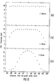
- Figs. 9(a), 9(b) and 9(c) there is shown the relationships between the positions on the Si wafer 5 and the film thickness of the epitaxial layers when the intersection point O' of the two gas-emitting-axis 8a and 9a is respectively positioned between the line connecting the center of the Si wafer 5 and the center of the nozzle tube 8 and the line connecting the center of the Si wafer and the center of the nozzle tube 9 and on the circle 85 having a radius ⁇ of 0 mm (i.e. just above the center of the Si wafer 5), 15 mm and 35 mm.
- the radius ⁇ of the circle 85 When the radius ⁇ of the circle 85 is 0 mm, the epitaxial growth at the periphery of the Si wafer is scarcely observed.
- ⁇ 15 mm, the film thickness in the center portion of 60 ⁇ 70 mm in diameter is uniformly thick, but that in the periphery is thin.
- ⁇ 35 mm, Si epitaxial layer is grown on the whole surface of the Si substrate 5 with uniform film thickness, the uniformity of the thickness being within 3%.
- the uniformity of the resistivity of the epitaxial layer is within 5% over the entire surface of the Si substrate 5.
- Si wafer 5 is installed to rotate around its center O. Near the Si wafer 5, three gas-supply nozzle tube 111, 112 and 113 are installed perpendicularly to the main surface of the Si wafer 5.
- a gas-emitting-axis 111a of starting-gases emitted from a gas-emission hole 114 formed in the nozzle tube 111 is tilted from the center O of the Si wafer 5 at an angle ⁇
- a gas-emitting-axis 113a of starting-gases emitted from a gas-emission hole 116 formed in the nozzle tube 113 being tilted from the center O of the Si wafer 5 at an angle ⁇ .
- the angles ⁇ , ⁇ and ⁇ are set not to be 0° and the intersection points O', O'' and O''' do not coincide with the center O of the Si wafer 5.
- the angles ⁇ , ⁇ and ⁇ are changed according to the size of the Si wafer 5 and the installation positions of the nozzle tubes 111, 112 and 113, the intersection points O', O'' and O''' being favorably positioned above the hatched region of the Si wafer 5 which is inside the semicircle of the Si wafer 5 on the nozzle-tube side and outside the concentric circle 85 having, a radius ⁇ ' which is 30% of a radius R' of the Si wafer 5 as the second embodiment.
- the Si wafer 5 having a diameter of 200 mm and the nozzle tubes 111, 112 and 113 are installed in the CVD apparatus shown in Fig. 1.
- the Si wafer 5 is held horizontally in the wafer holder 6.
- the wafer 5 is heated to 1100°C.
- SiH2Cl2, H2 and B2H6 (diluted with H2) are introduced through the nozzle tubes 111, 112 and 113, the flow rates of SiH2Cl2, H2 and B2H6 being 400 cc/min, 30 l/min and 20 cc/min, respectively. Under the pressure of ca.
- Figs. 12(a), 12(b) and 12(c) the relationships between the positions on the Si wafer 5 and the film thickness of the epitaxial layers when ⁇ ' is 0 mm, 25 mm and 65 mm are shown.
- ⁇ ' is 0 mm
- the film thickness only at the center portion of the Si wafer 5 is thick.
- ⁇ ' 25 mm
- the center portion is flat but the film thickness at the periphery is thin.
- ⁇ ' 60 mm, uniform film thickness is obtained, its uniformity being within ⁇ 3%.
- the number of the nozzle tube is three, good uniformity of the film thickness can be obtained on the Si wafer having a large diameter of more than 200 mm.
- an outer reaction tube 11 and an inner reaction tube 7 are installed on a pedestal 14.
- a wafer holder 6 for holding the Si wafers 5 is installed in the inner reaction tube 7.
- a gas-supply nozzle tube 130 is installed vertically near the wafer holder 6. Starting-gases are introduced through the nozzle tube 130 over the Si wafers 5 and exhaused through holes 10 formed in the wall of the inner reaction tube 7 and through a vent 12 formed in the outer reaction tube 11. The Si wafers 5 are heated by the furnace 13.
- gas-emission holes 131 are formed in the nozzle tube 130. Since the holes 131 are aligned in three columns, starting-gases emitted from the nozzle tube 130 spread in a radial manner over a wide area of the Si wafer 5. Therefore, uniform film thickness over the entire the Si wafer 5 having a large diameter can be obtained.
- Si wafers 5 having a diameter of 150 mm are set in the wafer holder 6, the space between the adjacent Si wafers 5 being 8 mm.
- the temperature inside the inner reaction tube 7 is elevated to 1050°C by the furnace 13.
- H2, SiH2Cl2 and PH3 are introduced into the inner reaction tube 7.
- the flow rate of H2 is 20 l/min, SiH2Cl2, 200 ml/min and PH3, 2 ml/min.
- N-type Si epitaxial layers are grown on the installed wafers 5 under a pressure of ca. 700 Pa (5 Torr).
- the uniformity of the film thickness is ⁇ 5% within the center portion of 60 mm in diameter and ⁇ 40% over the whole surface of the Si wafer 5.
- uniformity of the film thickness according to the present embodiment is remarkably improved to show the good flatness of ⁇ 4% in the film thickness over the whole surface of the Si wafer 5.
- the uniformity of the resistivity of the epitaxial layer is about 3% over the whole surface of the Si wafer 5.
- a nozzle tube 170 has three gas-supply planes 172, 173 and 174 facing the Si wafers 5. In each plane, the gas-supply holes 171 are formed in one column. Therefore, gas-emitting-axes 171a are spread in a radial manner above the Si wafer 5.
- Si epitaxial layers are grown on the Si wafers 5 of 150 mm in diameter by the nozzle tube 170 shown in Fig. 17, which is employed in the CVD apparatus shown in Fig. 13 in place of the nozzle tube 130 in the same growth condition as in the fourth embodiment.
- the uniformity of the film thickness on-the-wafer is ⁇ 4%, resulting in the same uniformity as the fourth embodiment.
- a nozzle tube 180 has a gas-emission tube 182 in which a plurality of gas-emission holes 181 are formed and a gas-inlet tube 183.
- the top end of the gas-inlet tube 183 is connected to the center portion of the gas-emission tube 182.
- the starting-gases are to be supplied from the bottom end of the gas-inlet tube 183. Since the starting-gases are supplied into the center portion of the gas emission tube 182, uniform flow rates of the starting-gases emitted from the gas-emission holes 181 are obtained regardless of the positions of the gas-emission holes 181 in the gas-emission tube 182, resulting in the excellent wafer-to-wafer uniformity.
- the nozzle tube 180 of Fig. 18 is installed in the innter reaction tube 7 in place of the nozzle tube 130.
- 100 Si wafers 5 of 150 mm in diameter are set in the wafer holder 6 with a spacing of 5 mm between adjacent Si wafers 5. Rotating the wafer holder 6 at 5 rpm, the temperature inside the inner reaction tube 7 is elevated to 1050°C by the furnace 13.
- H2Cl2 and PH3 are introduced into the inner reaction tube 7 with flow rates of 20 l/min of H2, 200 ml/min of SiH2Cl2 and 2 ml/min of PH3 to grow N-type Si epitaxial layers of 5 ⁇ m in thickness under a pressure of ca. 700 Pa (5 Torr).
- a good wafer-to-wafer uniformity of the film thickness is obtained for 50 Si wafers 5 set in the lower side of the wafer holder 6, but the film thickness decreases gradually as the setting position of the Si wafer 5 becomes close to the upper side, resulting in deteriorated wafer-to-wafer uniformity.
- the wafer-to-wafer uniformity of the film thickness according to the present invention is remarkably improved to show the wafer-to-wafer uniformity of 5% in the film thickness over the whole wafers 5 in the wafer holder 6.
- the wafer-to-wafer uniformity of the resistivity is also improved in the same manner as the film thickness.
- P-type Si epitaxial films are grown by introducing H2, SiH2Cl2 and B2H6 as starting gases with flow rate of 20 l/min of H2, 200 ml/min of SiH2Cl2 and 2 ml/min of B2H6. Epitaxial layers with excellent wafer-to-wafer uniformity can be grown also in this case.
- a gas-supply nozzle tube 200 has a main gas-supply nozzle tube 202 in which a plurality of gas-emission holes 201 are formed in a line, a branch gas-supply nozzle tube 203 of which the top and bottom ends are respectively connected to the top and bottom ends of the main gas-supply nozzle tube 202 and a gas-inlet nozzle tube 204.
- the top end of the gas-inlet nozzle tube 204 is connected to the center portion of the branch gas-supply nozzle tube 203 so as to supply starting-gases from the bottom end of the gas-inlet tube 204.
- the flow rate of the starting-gas mixture emitted from the gas-emission holes 201 is equalized regardless of positions of the gas-emission holes 201 in the main gas-supply nozzle tube 202, resulting in the good wafer-to-wafer uniformity of grown epitaxial layers.
- the nozzle tube 200 of Fig. 20 is installed in the inner reaction tube 7 in place of the nozzle tube 130.
- 100 Si wafers 5 of 150 mm in diameter are set in the wafer holder 6 with a spacing of 8 mm between the adjacent Si wafers 5.
- the temperature inside the inner reaction tube 7 is elevated to 1050°C by the furnace 13.
- H2, SiH2Cl2 and PH3 are introduced with flow rate of 20 l/min, 200 ml/min and 2 ml/min to grow N-type Si epitaxial layers of 5 ⁇ m in thickness under a pressure of ca. 700 Pa (5 Torr).
- a relationship between the setting-positions of the Si wafers 5 in the wafer holder 6 and the film thickness of the epitaxial layer grown in accordance with the present embodiment shown by a solid line
- that of the epitaxial layer grown by the nozzle tube 130' shown in Fig. 16 through which starting gases are supplied shown by a broken line.
- a good wafer-to-wafer uniformity of the film thickness is obtained for 50 Si wafers 5 set in the lower side of the wafer holder 6, but the film thickness decreases gradually toward the upper side wafer, resulting in a deteriorated wafer-to-wafer uniformity.
- the wafer-to-wafer uniformity of the film thickness grown in accordance with the present invention is remarkably improved to show the wafer-to-wafer uniformity of 5%.
- the wafer-to-wafer uniformity of the resistivity is also improved in the same manner as the film thickness.
- P-type Si epitaxial films are grown by introducing H2, SiH2Cl2 and B2H6 as starting-gases with flow rates of 20 l/min, 200 ml/min and 2 ml/min under the same growth condition as that in the case of PH3 except for the starting-gas of B2H6. Epitaxial layers having good wafer-to-wafer uniformity can also be grown.
- an outer reaction tube 11 having a vent 12 is installed on a pedestal 14.
- An inner reaction tube 7 having holes 10 for exhausting reaction gases is installed in the outer reaction tube 11 and on the pedestal 14.
- a wafer holder 6 holding Si wafers 5 in a stack-like fashion is installed rotatably in the inner reaction tube 7.
- Gas-supply nozzle tubes 221 and 222 are installed vertically near the wafer holder 6, the gas-supply nozzle tubes respectively having the same numbers of holes as the Si wafers 5.
- the Si wafers 5 are heated by the furnace 13.
- Si wafers 5 having a diameter of 150 mm are set in the wafer holder 6 with a spacing of 8 mm between adjacent Si wafers.
- H2 is introduced at a flow rate of 25 l/min through the nozzle tube 221
- Ar is at a flow rate of 20 l/min through the nozzle tube 222 at a flow rate of 20 l/min.
- the pressure in the reaction tubes 7 and 11 are kept at ca. 700 Pa (5 Torr). Under this condition, the temperature of the Si wafers is elevated to 1100°C.
- Si epitaxial layers are grown on the Si wafers 5 by introducing SiH2Cl2 and B2H6 through the nozzle tube 222 with flow rates of 600 ml/min and 0.01 ml/min, respectively, while keeping the pressure in the reaction tube 7 and 11 at ca. 700 Pa (5 Torr).
- Epitaxial films of 5 ⁇ m in film thickness are grown on all the 75 Si wafers 5.
- the uniformity of the film thickness was within ⁇ 4% and the uniformity of the resistivity was ⁇ 6%.
- H2 is introduced through the nozzle tube 222 at the flow rate of 20 l/min as a carrier gas in place of the Ar carrier gas, the uniformity of the film thickness of the epitaxial films is deteriorated to about ⁇ 12% and the variation of the resistivity of the epitaxial layer is increased to about 20%.
- the flow rate of the H2 carrier gas is required to be more than 120 l/min.
- N-type epitaxial layers are grown as another example of the present embodiment.
- Si epitaxial layers are grown on the Si wafers 5 by further introducing SiHCl3 and PH3 through the nozzle tube 222 with flow rates of 500 ml/min and 0.02 ml/min, respectively, while keeping the pressure in the reaction tubes 7 and 11 at ca. 1.1 kPa (8 Torr).
- Epitaxial films of 8 ⁇ m in thickness are grown on all the 75 Si wafers 5.
- the uniformity of the grown film thickness was within ⁇ 5% and the uniformity of the resistivity was within ⁇ 7%.
- H2 is introduced as a carrier gas through the nozzle tube 222 at the flow rate of 25 ml/min in place of Ar
- the uniformity of the film thickness of the epitaxial layers is deteriorated to about 15% and the variation of the resistivity of the epitaxial layer increases to about ⁇ 20%.
- the flow rate of the H2 carrier gas is required to be more than 180 l/min.
- the apparatus to supply H2 and the apparatus to treat the exhaust gases can be miniaturized to lower the manufacturing-cost.
- the foregoing embodiments represent the cases where Si epitaxial layers are grown on the Si wafers, but the CVD apparatus according to the present invention can be used to grown an oxide-film, a nitride-film, a polysilicon film, an amorphous silicon film and other inorganic films. Furthermore, besides the resistance heating method, a RF-induction-heating method and a radiant-heating method may be similarly used to heat the substrates such as Si wafers.
Landscapes
- Chemical & Material Sciences (AREA)
- Chemical Kinetics & Catalysis (AREA)
- General Chemical & Material Sciences (AREA)
- Engineering & Computer Science (AREA)
- Crystallography & Structural Chemistry (AREA)
- Materials Engineering (AREA)
- Metallurgy (AREA)
- Organic Chemistry (AREA)
Description
- The present invention relates to a chemical vapor deposition (CVD) apparatus and, more particularly, to a CVD apparatus for silicon epitaxial growth.
- A demand for Si epitaxial wafers (Si wafers with epitaxial films) has been enhanced to obtain high quality bipolar, Bi-CMOS, CCD and other semiconductor devices. Additionally, diameters of the Si wafers have become as large as 125 mm to 150 mm(5 to 6 inches) to reduce the process costs. However, since a wafer-processing capacity of the conventional CVD apparatus was small, a large number of Si wafers of large diameters could not be treated simultaneously, resulting in the expensive cost for manufacturing epitaxial wafers. Moreover, the uniform film thickness and the uniform crystal quality could not be obtained over the entire Si wafer of large diameter.
- For improving a growth of the uniform epitaxial layer on the Si wafer of large diameter, a CVD apparatus was proposed in Japanese Laid open patent 62-173712. In this CVD apparatus, Si wafers having diameters of 150 mm (6 inches) were vertically stacked in a wafer holder. To obtain a uniformity of the epitaxial layers, the wafer holder was rotated so as to supply the starting gases on the Si wafers through holes of a gas-supply nozzle tube, the direction of the holes being deviated from the rotation center of each Si wafer. In this CVD apparatus, however, the number of the gas-supply nozzle tube was only one. Thus, the flow of the starting gases over the Si wafer was still nonuniform, especially over the Si wafer of a large diameter. Therefore, the obtained uniformity of the epitaxial layer does not have a level required for using for large-scale integrated circuits.
- From EP-A-0 164 928 there has been known a CVD-apparatus as defined in the preamble portion of
claim 1. This prior art apparatus has three parallel gas-supply nozzle tubes or manifolds directed towards the center of rotation of the substrates. The degree of uniformity of the deposited layer obtained with this apparatus is not reported. - It is an object of the invention to provide a CVD-apparatus of the abovementioned kind by which an improved uniformity of epitaxial layers on the substrates, particularly on Si-waivers having a large diameter, can be obtained.
- According to the invention, this object is achieved with the CVD-apparatus as defined in
claim 1. The dependent claims 2 to 5 specify further advantageous features of the apparatus according to the invention. - Since the starting-gases are supplied from the two nozzle tubes and the gas-emitting-axes from the two nozzle tubes intersect each other at the point deviated from the center of the Si wafer, the flow of the starting-gases become uniform over the Si wafers having large diameters. To obtain more uniform gas flow, a third gas-supply nozzle tube may be added to the first and second gas-supply nozzle tubes, the two gas-emitting-axes of the gas-emission holes of the first and third gas-supply nozzle tubes and the two gas-emitting-axes of the second and third gas-supply nozzle tubes respectively intersecting each other over the Si wafer and these intersections being also deviated from the center of each Si wafer.
- The gas-emission holes may be formed in the plural columns, each of the columns having the gas-emission holes in a vertical direction. The gas-supply nozzle tube favorably has gas-inlet portions at its both ends. The gas-supply nozzle tube also favorably has gas inlet portion at its center.
- The above and further objects, features and advantages of the present invention will become more apparent from the following detailed description taken in conjunction with the accompanying drawings, wherein:
- Fig. 1 is a sectional view showing a CVD apparatus in accordance with the first embodiment of the present invention;
- Fig. 2(a) is a sectional view for explaining a nozzle tube used in the first embodiment of the present invention;
- Fig. 2(b) is a sectional view along A-A′ line in Fig. 2(a);
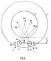
- Fig. 3 is a sectional view for explaining an arrangement of the nozzle tubes used in the first embodiment of the present invention;
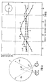
- Fig. 4(a) is a diagram showing a relationship between the positions on the Si wafer and the growth rate of the epitaxial layer and a relationship between the positions on the Si wafer and the resistivity of the epitaxial layer in accordance with the first embodiment of the present invention;
- Fig. 4(b) is a diagram showing a relationship between the positions on the Si wafer and the growth rate of the epitaxial layer and for explaining the uniformity of the epitaxial layer in accordance with the first embodiment of the present invention;
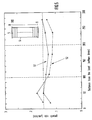
- Fig. 5 is a diagram showing a relationship between the positions of the Si wafer in the wafer holder and the growth rate of the epitaxial layer;
- Fig. 6(a) is a front view of the nozzle tube used in obtaining the reference data shown in Fig. 5;
- Fig. 6(b) is a sectional view of the nozzle tube shown in Fig. 6(a);
- Fig. 7 is a diagram showing a relationship between the positions on the Si wafer and the resistivity of the epitaxial layers and for explaining the effect of the carrier gas;
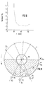
- Fig. 8 is a sectional view for explaining a second embodiment of the present invention;
- Figs. 9(a), 9(b) and 9(c) are diagrams showing relationships between the positions on the Si wafer and the film thickness of the epitaxial layers in accordance with the second embodiment of the present invention;
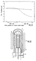
- Fig. 10 is a diagram showing a relationship between the positions of the intersections of the gas-emitting-axes from the nozzle tubes and the deviation of the film thickness of the epitaxial layers;
- Fig. 11 is a sectional view for explaining a third embodiment of the present invention;
- Figs. (12a), 12(b) and 12(c) are diagrams showing relationships between the positions on the Si wafers and the film thickness of the epitaxial layers in accordance with the third embodiment of the present invention;
- Fig. 13 is a sectional view showing a CVD apparatus in accordance with the fourth embodiment of the present invention;
- Fig. 14(a) is a front view showing a nozzle tube used in the fourth embodiment of the present invention;
- Fig. 14(b) is a sectional view along A-A′ line of the nozzle tube shown in Fig. 14(a);
- Fig. 15 is a diagram showing a relationship between the positions on the Si wafer and the film thickness of the epitaxial layer in accordance with the fourth embodiment of the present invention;
- Fig. 16(a) is a front view of the nozzle tube used in obtaining the reference data shown in Fig. 15;
- Fig. 16(b) is a sectional view of the nozzle tube shown in Fig. 16(a);
- Fig. 17(a) is a sectional view for explaining the fifth embodiment of the present invention;
- Fig. 17(b) is a front view of the nozzle tube used in the fifth embodiment of the present invention;
- Fig. 17(c) is a sectional view of the nozzle tube shown in Fig. 17(b);
- Fig. 18 is a front view of the nozzle tube used in the sixth embodiment of the present invention;
- Fig. 19 is a diagram showing a relationship between the positions of the Si wafers and the film thickness of the epitaxial layers in accordance with the sixth embodiment of the present invention;
- Fig. 20 is a front view of the nozzle tube used in the seventh embodiment of the present invention;
- Fig. 21 is a diagram showing a relationship between the positions of the Si wafers and the film thickness of the epitaxial layers in accordance with the seventh embodiment of the present invention; and
- Fig. 22 is a sectional view showing a CVD apparatus used in the eighth embodiment of the present invention.
- Referring to Fig. 1, an
outer reaction tube 11 and aninner reaction tube 7 having an inner diameter of 240 mm are installed on apedestal 14. Awafer holder 6 is installed in theinner reaction tube 7. In thewafer holder 6, 30 Si wafers 5 having a diameter of 150 mm (6 inches) are piled in a vertical direction with a space of 10 mm. Gas-supply nozzle tubes wafer holder 6. Starting-gases are introduced through thenozzle tubes holes 10 formed in the wall of theinner reaction tube 7 and avent 12 formed in theouter reaction tube 11. The Siwafers 5 are heated by a resistance-heating furnace 13. - Referring to Fig. 2(a) and 2(b), a typical form of the
nozzle tube 9 is shown and is formed of amain nozzle tube 91 having an inner diameter of 20 mm and having gas-emission holes branch nozzle tube 92 of an inner diameter of 10 mm, and a gas-inlet tube 93 of an inner diameter of 10 mm connected to both the bottom ends of the main andbranch nozzle tubes branch nozzle tube 92 are respectively connected to the top end and the bottom end of themain nozzle tube 91. The interval of the gas-emission holes holes adjacent Si wafers 5 to introduce the starting-gases over eachSi wafer 5. - Referring now to Fig. 3, the
nozzle tube 8 has amain nozzle tube 81 and abranch nozzle tube 82 and has a similar structure to thenozzle tube 9 but has only one gas-supply column in which many gas-emission holes 83 are formed in the vertical direction. The space L between the edge of theSi wafer 5 and the centers of thenozzle tube Si wafer 5 and the center of themain nozzle tube 81 intersects the line connecting the center of theSi wafer 5 and the center of themain nozzle tube 91 with an angle of 30°. - A gas-emitting-
axis 83a of a gas blown from the gas-emission hole 83 (hereinafter, the line connecting the center of a main nozzle tube and the center of a gas-emission hole formed in the wall of the main nozzle tube is referred to as a gas-emitting-axis of its gas-emission hole; therefore, in this case, this gas-emitting-axis 83a of the gas-emission hole 83 is identical with the line connecting the center of themain nozzle 81 and the center of the gas-emission hole 83) is deviated from the center ofSi wafer 5 toward its left-hand side. The angle of this gas-emitting-axis 83a formed with the line connecting both the centers of theSi wafer 5 and themain nozzle tube 81 is designed at 15°. A gas-emitting-axis 94a of the gas-emission hole 94 passes just above the center of theSi wafer 5. A gas-emitting-axis 95a of the gas-emission hole 95 is deviated from the center of theSi wafer 5 toward its right-hand side. The angle between this gas-emitting-axis 95a and the line connecting both the centers of theSi wafer 5 and themain nozzle 91 is designed at 15°. A gas-emitting-axis 96a of the gas-emission hole 96 is deviated from the center of theSi wafer 5 toward its right-hand side. The angle between this gas-emitting-axis 96a and the line connecting both the centers of theSi wafer 5 and themain nozzle 91 is designed at 30°. - Referring back to Fig. 1 and Fig. 3, a mixture of Ar, SiH₂Cℓ₂, HCℓ and PH₃ is introduced into the
inner reaction tube 7 through thenozzle tube 9, together with H₂ introduced through thenozzle tube 8. Flow rates of Ar, SiH₂Cℓ₂, HCℓ and H₂ are respectively controlled at 20 ℓ/min, 400 cc/min, 300 cc/min and 20 ℓ/min. PH₃ of 50 ppm in Ar is 300 times diluted by H₂ and thus diluted gas is introduced at a flow rate of 50 cc/min. Epitaxial growth is carried out at 1,000°C, keeping the total pressure in theinner reaction tube 7 at ca. 1,3 kPa (10 Torr). The film thickness of the epitaxial layer is measured by an IR interference method, the resistivity of the epitaxial layer being measured by a four-point probe technique. - Referring now to Fig. 4(a), the epitaxial layer obtained in accordance with the present embodiment shows an excellent uniformity. That is, both the uniformity on a wafer of the growth rate of the epitaxial layer and the uniformity on the wafer of the resistivity of the epitaxial layer were within ±5%. Referring to Fig. 4(b) and Fig. 4(c), uniformity of the growth rate of the epitaxial layer grown in accordance with the present embodiment (see curve 41) is superior to that of the epitaxial layer grown by a gas-
supply nozzle tube 45 of one gas-emission holes 46 shown in Fig. 4(c). Acurve 42 was obtained by setting the gas-emitting-axis 46a of the gas-emission hole 46 passing just above the center of theSi wafer 5, and a curve 43 was obtained by setting the gas-emitting-axis 46a of the gas-emission hole 46 so as to deviate from the center of theSi wafer 5 toward its right-hand side, the angle between this gas-emitting-axis 46a and the line connecting both the centers of theSi wafer 5 and thenozzle tube 45 being 15°, the gas-emitting-axis 83a being deviated from the center of theSi wafer 5 toward its left-hand side, the angle of the gas-emitting-axis 83a and the line connecting both the centers of theSi wafer 5 and thenozzle tube 81 being 15°. In the process for obtaining thesecurves 42 and 43, H₂ is introduced by thenozzle tube 81 at a flow rate of 20 ℓ/min together with Ar, SiH₂Cℓ₂, HCℓ and PH₃ introduced through thenozzle tube 45 at flow rates of 12 ℓ/min, 400 cc/min, 300 cc/min and 50 cc/min, respectively. - Referring to Fig. 5 and Fig. 6, wafer-to-wafer uniformity of the growth rate of the epitaxial layer grown in accordance with the present embodiment (see curve 51) is excellent and superior to that of the epitaxial layer (see curve 52) grown by using the gas-
supply nozzle tube 61 shown in Fig. 6 in place of thenozzle tube 9 shown in Figs. 1 and 3. Thenozzle tube 61 has no branch nozzle tube such as thebranch nozzle tube 92 of thenozzle tube 9 so as to introduce starting-gases only from the bottom end of thenozzle tube 61. - Referring now to Fig. 7, when H₂ is used as a carrier gas in place of Ar, uniformity on a wafer of the resistivity of the epitaxial layer is deteriorated to have ±150%. Since mass and viscosity of hydrogen are smaller than those of Ar, PH₃ is not sufficiently transported by H₂ carrier gas. Moreover, when H₂ is used as a carrier gas, stagnant layer above the
Si wafer 5 is thin to consume PH₃ at the peripheral of theSi wafer 5. Therefore, the resistivity of the epitaxial layer becomes small at the peripheral of the Si wafer and large at the center of the Si wafer, resulting in large variation of the resistivity of the epitaxial layer. - Referring to fig. 8,
Si wafer 5 is installed to be rotated, as a rotation center coincident with the center O of theSi wafer 5. Near theSi wafer 5, two gas-supply nozzle tubes Si wafer 5. A gas-emitting-axis 88a of starting-gases emitted from the gas-emission hole 88 formed in thenozzle tube 8 is tilted from the center O of theSi wafer 5 at an angle of ω, a gas-emitting-axis 89a of starting-gases emitted from a gas-emission hole 98 formed in thenozzle tube 9 being tilted from the center O of theSi wafer 5 at an angle of ϑ. - The angles ω and ϑ are set not to be 0° and the intersection point O′ of the two gas-emitting-
axes Si wafer 5. The angles ω and ϑ need to be changed according to the size of theSi wafer 5 and the installation positions of thenozzle tubes nozzle tubes Si wafers 5, the film thickness at the center of theSi wafer 5 becomes thick, while the film thickness at the periphery of theSi wafer 5 becomes thin. Therefore, the intersection point O' is favorably positioned above the hatched region of theSi wafer 5 which is inside the semicircle of theSi wafer 5 on the nozzle-tube side and outside aconcentric circle 85 having a radius γ which is 30% of a radius R of theSi wafer 5. - The
Si wafer 5 having a diameter of 150 mm and thenozzle tubes Si wafer 5 is held horizontally in thewafer holder 6. Rotating the wafer holder at 5 rpm, the temperature is elevated to 1100°C. SiH₂Cℓ₂, H₂ and PH₃ (diluted with H₂) are introduced by thenozzle tube - In Figs. 9(a), 9(b) and 9(c), there is shown the relationships between the positions on the
Si wafer 5 and the film thickness of the epitaxial layers when the intersection point O' of the two gas-emitting-axis 8a and 9a is respectively positioned between the line connecting the center of theSi wafer 5 and the center of thenozzle tube 8 and the line connecting the center of the Si wafer and the center of thenozzle tube 9 and on thecircle 85 having a radius γ of 0 mm (i.e. just above the center of the Si wafer 5), 15 mm and 35 mm. - When the radius γ of the
circle 85 is 0 mm, the epitaxial growth at the periphery of the Si wafer is scarcely observed. When γ is 15 mm, the film thickness in the center portion of 60 ∼ 70 mm in diameter is uniformly thick, but that in the periphery is thin. When γ is 35 mm, Si epitaxial layer is grown on the whole surface of theSi substrate 5 with uniform film thickness, the uniformity of the thickness being within 3%. Moreover, when γ is 35 mm, the uniformity of the resistivity of the epitaxial layer is within 5% over the entire surface of theSi substrate 5. In Fig. 10, the relationship between the radius γ of thecircle 85 and the variation of the film thickness of the epitaxial layer over the entire surface of theSi substrate 5 is shown. When γ is less than 25 mm, the variation of the film thickness increases abruptly. Moreover, when γ is less than 22.5 mm (which corresponds to 30% of the radius R of theSi wafer 5 of 150 mm in diameter), the variation of the film thickness is so large that the epitaxial film cannot be practically used in an IC production. When the epitaxial layer is grown by setting the intersection point O′ in the hatched region in Fig. 8, uniformity of the film thickness and the resistivity of the epitaxial layer is similar to the aformentioned results. - Referring to Fig. 11,
Si wafer 5 is installed to rotate around its center O. Near theSi wafer 5, three gas-supply nozzle tube Si wafer 5. A gas-emitting-axis 111a of starting-gases emitted from a gas-emission hole 114 formed in thenozzle tube 111 is tilted from the center O of theSi wafer 5 at an angle α, a gas-emitting-axis 112a of starting-gases emitted from a gas-emission hole 115 formed in thenozzle tube 112 being tilted from the center O of theSi wafer 5 at an angle β, a gas-emitting-axis 113a of starting-gases emitted from a gas-emission hole 116 formed in thenozzle tube 113 being tilted from the center O of theSi wafer 5 at an angle γ. - The angles α, β and γ are set not to be 0° and the intersection points O', O'' and O''' do not coincide with the center O of the
Si wafer 5. The angles α, β and γ are changed according to the size of theSi wafer 5 and the installation positions of thenozzle tubes Si wafer 5 which is inside the semicircle of theSi wafer 5 on the nozzle-tube side and outside theconcentric circle 85 having, a radius γ' which is 30% of a radius R' of theSi wafer 5 as the second embodiment. - The
Si wafer 5 having a diameter of 200 mm and thenozzle tubes Si wafer 5 is held horizontally in thewafer holder 6. Rotating the wafer holder at 8 rpm, thewafer 5 is heated to 1100°C. SiH₂Cℓ₂, H₂ and B₂H₆ (diluted with H₂) are introduced through thenozzle tubes Si wafer 5 and the center of thenozzle tube 111 and the line connecting the center of theSi wafer 5 and the center of thenozzle tube 113 and on thecircle 85 having a radius γ'. - In Figs. 12(a), 12(b) and 12(c), the relationships between the positions on the
Si wafer 5 and the film thickness of the epitaxial layers when γ' is 0 mm, 25 mm and 65 mm are shown. When γ' is 0 mm, the film thickness only at the center portion of theSi wafer 5 is thick. When γ' is 25 mm, the center portion is flat but the film thickness at the periphery is thin. When γ' is 60 mm, uniform film thickness is obtained, its uniformity being within ±3%. - In this embodiment, since the number of the nozzle tube is three, good uniformity of the film thickness can be obtained on the Si wafer having a large diameter of more than 200 mm.
- Referring now to Fig. 13, an
outer reaction tube 11 and aninner reaction tube 7 are installed on apedestal 14. Awafer holder 6 for holding theSi wafers 5 is installed in theinner reaction tube 7. A gas-supply nozzle tube 130 is installed vertically near thewafer holder 6. Starting-gases are introduced through thenozzle tube 130 over theSi wafers 5 and exhaused throughholes 10 formed in the wall of theinner reaction tube 7 and through avent 12 formed in theouter reaction tube 11. TheSi wafers 5 are heated by thefurnace 13. - Referring to Figs. 14(a) and 14(b), many gas-
emission holes 131 are formed in thenozzle tube 130. Since theholes 131 are aligned in three columns, starting-gases emitted from thenozzle tube 130 spread in a radial manner over a wide area of theSi wafer 5. Therefore, uniform film thickness over the entire theSi wafer 5 having a large diameter can be obtained. - Referring to Fig. 13, 100
Si wafers 5 having a diameter of 150 mm are set in thewafer holder 6, the space between theadjacent Si wafers 5 being 8 mm. Rotating thewafer holder 6 at 5 rpm, the temperature inside theinner reaction tube 7 is elevated to 1050°C by thefurnace 13. Through thenozzle tube 130, H₂, SiH₂Cℓ₂ and PH₃ are introduced into theinner reaction tube 7. The flow rate of H₂ is 20 ℓ/min, SiH₂Cℓ₂, 200 mℓ/min and PH₃, 2 mℓ/min. N-type Si epitaxial layers are grown on the installedwafers 5 under a pressure of ca. 700 Pa (5 Torr). - In Fig. 15, a relationship between the positions on the
Si wafer 5 and the film thickness of the epitaxial layer according to the present embodiment (shown by a solid line) along with that of the epitaxial layer grown by the nozzle tube 130' shown in Fig. 16 having gas-emission holes 131' in one column in place of the nozzle tube 130 (shown by a broken line). In a case of using the nozzle tube 130' shown in Fig. 16, the uniformity of the film thickness is ±5% within the center portion of 60 mm in diameter and ±40% over the whole surface of theSi wafer 5. However, uniformity of the film thickness according to the present embodiment is remarkably improved to show the good flatness of ±4% in the film thickness over the whole surface of theSi wafer 5. Moreover, the uniformity of the resistivity of the epitaxial layer is about 3% over the whole surface of theSi wafer 5. - Referring to Fig. 17, a
nozzle tube 170 has three gas-supply planes Si wafers 5. In each plane, the gas-supply holes 171 are formed in one column. Therefore, gas-emitting-axes 171a are spread in a radial manner above theSi wafer 5. - Si epitaxial layers are grown on the
Si wafers 5 of 150 mm in diameter by thenozzle tube 170 shown in Fig. 17, which is employed in the CVD apparatus shown in Fig. 13 in place of thenozzle tube 130 in the same growth condition as in the fourth embodiment. The uniformity of the film thickness on-the-wafer is ±4%, resulting in the same uniformity as the fourth embodiment. - Referring to Fig. 18, a
nozzle tube 180 has a gas-emission tube 182 in which a plurality of gas-emission holes 181 are formed and a gas-inlet tube 183. The top end of the gas-inlet tube 183 is connected to the center portion of the gas-emission tube 182. The starting-gases are to be supplied from the bottom end of the gas-inlet tube 183. Since the starting-gases are supplied into the center portion of thegas emission tube 182, uniform flow rates of the starting-gases emitted from the gas-emission holes 181 are obtained regardless of the positions of the gas-emission holes 181 in the gas-emission tube 182, resulting in the excellent wafer-to-wafer uniformity. - Referring to Fig. 13 again, the
nozzle tube 180 of Fig. 18 is installed in theinnter reaction tube 7 in place of thenozzle tube 130. 100Si wafers 5 of 150 mm in diameter are set in thewafer holder 6 with a spacing of 5 mm betweenadjacent Si wafers 5. Rotating thewafer holder 6 at 5 rpm, the temperature inside theinner reaction tube 7 is elevated to 1050°C by thefurnace 13. Through thenozzle tube 180, H₂, SiH₂Cℓ₂ and PH₃ are introduced into theinner reaction tube 7 with flow rates of 20 ℓ/min of H₂, 200 mℓ/min of SiH₂Cℓ₂ and 2 mℓ/min of PH₃ to grow N-type Si epitaxial layers of 5 µm in thickness under a pressure of ca. 700 Pa (5 Torr). - In Fig. 19, a relationship between the setting-positions of the
Si wafers 5 in thewafer holder 6 and the film thickness of the grown epitaxial layer according to the present embodiment (shown by a solid line) along with that of the epitaxial layer grown by the nozzle tube 130' shown in Fig. 16 in which starting-gases are supplied only through the bottom end of the nozzle tube 130' (shown by a broken line). In a case of using the nozzle tube 130' shown in Fig. 16, a good wafer-to-wafer uniformity of the film thickness is obtained for 50Si wafers 5 set in the lower side of thewafer holder 6, but the film thickness decreases gradually as the setting position of theSi wafer 5 becomes close to the upper side, resulting in deteriorated wafer-to-wafer uniformity. However, the wafer-to-wafer uniformity of the film thickness according to the present invention is remarkably improved to show the wafer-to-wafer uniformity of 5% in the film thickness over thewhole wafers 5 in thewafer holder 6. The wafer-to-wafer uniformity of the resistivity is also improved in the same manner as the film thickness. - Next, P-type Si epitaxial films are grown by introducing H₂, SiH₂Cℓ₂ and B₂H₆ as starting gases with flow rate of 20 ℓ/min of H₂, 200 mℓ/min of SiH₂Cℓ₂ and 2 mℓ/min of B₂H₆. Epitaxial layers with excellent wafer-to-wafer uniformity can be grown also in this case.
- Referring to Fig. 20, a gas-
supply nozzle tube 200 has a main gas-supply nozzle tube 202 in which a plurality of gas-emission holes 201 are formed in a line, a branch gas-supply nozzle tube 203 of which the top and bottom ends are respectively connected to the top and bottom ends of the main gas-supply nozzle tube 202 and a gas-inlet nozzle tube 204. The top end of the gas-inlet nozzle tube 204 is connected to the center portion of the branch gas-supply nozzle tube 203 so as to supply starting-gases from the bottom end of the gas-inlet tube 204. Since the starting-gases are supplied to both the top and bottom ends of the main gas-supply nozzle tube 202 through thebranch nozzle tube 203, the flow rate of the starting-gas mixture emitted from the gas-emission holes 201 is equalized regardless of positions of the gas-emission holes 201 in the main gas-supply nozzle tube 202, resulting in the good wafer-to-wafer uniformity of grown epitaxial layers. - Referring back to Fig. 13, the
nozzle tube 200 of Fig. 20 is installed in theinner reaction tube 7 in place of thenozzle tube 130. 100Si wafers 5 of 150 mm in diameter are set in thewafer holder 6 with a spacing of 8 mm between theadjacent Si wafers 5. Rotating thewafer holder 6 at 5 rpm, the temperature inside theinner reaction tube 7 is elevated to 1050°C by thefurnace 13. Through thenozzle tube 200, H₂, SiH₂Cℓ₂ and PH₃ are introduced with flow rate of 20 ℓ/min, 200 mℓ/min and 2 mℓ/min to grow N-type Si epitaxial layers of 5 µm in thickness under a pressure of ca. 700 Pa (5 Torr). - In Fig. 21, a relationship between the setting-positions of the
Si wafers 5 in thewafer holder 6 and the film thickness of the epitaxial layer grown in accordance with the present embodiment (shown by a solid line), along with that of the epitaxial layer grown by the nozzle tube 130' shown in Fig. 16 through which starting gases are supplied (shown by a broken line). In a case of using the nozzle tube 130' shown in Fig. 16, a good wafer-to-wafer uniformity of the film thickness is obtained for 50Si wafers 5 set in the lower side of thewafer holder 6, but the film thickness decreases gradually toward the upper side wafer, resulting in a deteriorated wafer-to-wafer uniformity. However, the wafer-to-wafer uniformity of the film thickness grown in accordance with the present invention is remarkably improved to show the wafer-to-wafer uniformity of 5%. The wafer-to-wafer uniformity of the resistivity is also improved in the same manner as the film thickness. - Next, P-type Si epitaxial films are grown by introducing H₂, SiH₂Cℓ₂ and B₂H₆ as starting-gases with flow rates of 20 ℓ/min, 200 mℓ/min and 2 mℓ/min under the same growth condition as that in the case of PH₃ except for the starting-gas of B₂H₆. Epitaxial layers having good wafer-to-wafer uniformity can also be grown.
- Referring now to Fig. 22, an
outer reaction tube 11 having avent 12 is installed on apedestal 14. Aninner reaction tube 7 havingholes 10 for exhausting reaction gases is installed in theouter reaction tube 11 and on thepedestal 14. Awafer holder 6 holdingSi wafers 5 in a stack-like fashion is installed rotatably in theinner reaction tube 7. Gas-supply nozzle tubes wafer holder 6, the gas-supply nozzle tubes respectively having the same numbers of holes as theSi wafers 5. TheSi wafers 5 are heated by thefurnace 13. - 75
Si wafers 5 having a diameter of 150 mm are set in thewafer holder 6 with a spacing of 8 mm between adjacent Si wafers. Rotating thewafer holder 6 at 10 rpm, H₂ is introduced at a flow rate of 25 ℓ/min through thenozzle tube 221, and Ar is at a flow rate of 20 ℓ/min through thenozzle tube 222 at a flow rate of 20 ℓ/min. The pressure in thereaction tubes Si wafers 5 by introducing SiH₂Cℓ₂ and B₂H₆ through thenozzle tube 222 with flow rates of 600 mℓ/min and 0.01 mℓ/min, respectively, while keeping the pressure in thereaction tube - Epitaxial films of 5 µm in film thickness are grown on all the 75
Si wafers 5. The uniformity of the film thickness was within ±4% and the uniformity of the resistivity was ±6%. When H₂ is introduced through thenozzle tube 222 at the flow rate of 20 ℓ/min as a carrier gas in place of the Ar carrier gas, the uniformity of the film thickness of the epitaxial films is deteriorated to about ±12% and the variation of the resistivity of the epitaxial layer is increased to about 20%. To obtain the same uniformity of the film thickness and the resistivity as the Ar carrier gas, the flow rate of the H₂ carrier gas is required to be more than 120 ℓ/min. - Next, using the same CVD apparatus shown in Fig. 22, N-type epitaxial layers are grown as another example of the present embodiment. Rotating 75
Si wafers 5 having a diameter of 150 mm at 10 rpm, H₂ is introduced at a flow rate of 35 ℓ/min through thenozzle tube 221 and Kr is introduced as a carrier gas of SiHCℓ₃ through thenozzle tube 222 at a flow rate 18 ℓ/min, while the pressure in thereaction tubes Si wafers 5 by further introducing SiHCℓ₃ and PH₃ through thenozzle tube 222 with flow rates of 500 mℓ/min and 0.02 mℓ/min, respectively, while keeping the pressure in thereaction tubes - Epitaxial films of 8 µm in thickness are grown on all the 75
Si wafers 5. The uniformity of the grown film thickness was within ±5% and the uniformity of the resistivity was within ±7%. When H₂ is introduced as a carrier gas through thenozzle tube 222 at the flow rate of 25 mℓ/min in place of Ar, the uniformity of the film thickness of the epitaxial layers is deteriorated to about 15% and the variation of the resistivity of the epitaxial layer increases to about ±20%. In order to obtain the same uniformity of the film thickness and the resistivity of the epitaxial layers as in the case of using Ar carrier gas, the flow rate of the H₂ carrier gas is required to be more than 180 ℓ/min. - In this example, since Kr having a larger atomic weight than Ar is used as a carrier gas of SiHCℓ₃ having a larger molecular weight than SiH₂Cℓ₂, the quantity of the carrier gas necessary to obtain uniform epitaxial layers can be reduced. Additionally, in the first example of the present embodiment, when Kr is used in place of Ar introduced with a flow rate of 20 ℓ/min, the reduced flow rate of 12 ℓ/min is enough to obtain the good uniformities in the film thickness and the resistivity.
- By using rare gases such as Ar and Kr, maintaining the uniformities of the film thickness and the resistivity, the amount of H₂ can be remarkably reduced. Therefore, the apparatus to supply H₂ and the apparatus to treat the exhaust gases can be miniaturized to lower the manufacturing-cost.
- The foregoing embodiments represent the cases where Si epitaxial layers are grown on the Si wafers, but the CVD apparatus according to the present invention can be used to grown an oxide-film, a nitride-film, a polysilicon film, an amorphous silicon film and other inorganic films. Furthermore, besides the resistance heating method, a RF-induction-heating method and a radiant-heating method may be similarly used to heat the substrates such as Si wafers.
Claims (5)
- A chemical vapor deposition apparatus comprising:
A reaction tube (7, 11);
a substrate-holder (6) in said reaction tube, said substrate-holder holding a stack of substrates (5) in predetermined horizontally arranged, vertically spaced positions;
rotating means for rotating said substrate holder (6) about a vertical axis whereby each of the substrates is rotated about a rotation center;
heating means (13) for heating the substrates;
a first gas-supply nozzle tube (81) extending vertically in said reaction tube (7, 11) and having a plurality of first gas-emission holes vertically spaced along a vertical line of holes, and a second gas-supply nozzle tube (91) extending vertically in said reaction tube (7, 11) and having a plurality of second gas-emission holes (94) vertically spaced along a vertical line of holes, the direction of gas-emission from each of said first and second gas-emission holes (83, 94) being substantially horizontal and along respective gas-emission axes (83A, 94A) intersecting each other at a point of intersection over the substrates, characterized in that said intersection point is off-set from the rotation center of the substrates (5). - A chemical vapor deposition apparatus as claimed in claim 1, wherein said substrate holder (5) is adapted to hold circular substrates (5) and wherein said point of intersection is positioned over a portion of each circular substrate (5) which is inside the semicircle of the substrate on the side of said first and second gas-supply nozzle (81, 91) and outside a circle (85) concentric with the circular substrate and having a radius of 30 % of the radius of the circular substrate.
- A chemical vapor deposition apparatus as claimed in claim 1 or 2, wherein said second gas-supply nozzle tube (91) comprises a plurality of second, third and fourth gas-emission holes (94, 95, 96) vertically spaced along three parallel vertical lines of holes, respectively, the directions of gas-emission from said second, third and fourth gas emission holes (94, 95, 96) being substantially horizontal and along second, third and fourth gas-emission axes (94a, 95a, 96a) which are angularly diverging and intersect with said first gas-emission axis (83A) at respective points of intersection over the substrate (5) which are off-set from the rotation center of the substrate.
- A chemical vapor deposition apparatus as claimed in any of claims 1 to 3, wherein the vertical spacings between adjacent ones of said first, second, third and/or fourth gas-emission holes (83, 94, 95, 96) are the same as the vertical spacings between the substrates (5) held by the substrate holder (6).
- A chemical vapor deposition apparatus as claimed in any of claims 1 to 4, wherein said first gas-supply nozzle tube (81, 202) and/or said second gas-supply nozzle tube (91) has a respective branch tube (82, 202, 92) extending parallel therewith, the top and bottom ends of the first and/or second gas-supply nozzle tube (81, 202, 91) being connected with the top and bottom ends, respectively, of the corresponding branch tube (82, 203, 92) and the branch tube being connected to a gas-supply tube (93, 204) at its bottom end or intermediate its ends.
Applications Claiming Priority (10)
| Application Number | Priority Date | Filing Date | Title |
|---|---|---|---|
| JP239605/87 | 1987-09-22 | ||
| JP239607/87 | 1987-09-22 | ||
| JP23960587A JPS6481215A (en) | 1987-09-22 | 1987-09-22 | Vapor growth apparatus |
| JP239603/87 | 1987-09-22 | ||
| JP62239607A JPH0670979B2 (en) | 1987-09-22 | 1987-09-22 | Vapor phase growth equipment |
| JP23960387 | 1987-09-22 | ||
| JP247176/87 | 1987-09-29 | ||
| JP24717687A JPS6489320A (en) | 1987-09-29 | 1987-09-29 | Vapor growth method |
| JP62553/88 | 1988-03-15 | ||
| JP6255388A JPH01235236A (en) | 1988-03-15 | 1988-03-15 | Vapor growth equipment |
Publications (3)
| Publication Number | Publication Date |
|---|---|
| EP0308946A2 EP0308946A2 (en) | 1989-03-29 |
| EP0308946A3 EP0308946A3 (en) | 1990-12-12 |
| EP0308946B1 true EP0308946B1 (en) | 1993-11-24 |
Family
ID=27523713
Family Applications (1)
| Application Number | Title | Priority Date | Filing Date |
|---|---|---|---|
| EP88115622A Expired - Lifetime EP0308946B1 (en) | 1987-09-22 | 1988-09-22 | Chemical vapor deposition apparatus for obtaining high quality epitaxial layer with uniform film thickness |
Country Status (3)
| Country | Link |
|---|---|
| US (1) | US4992301A (en) |
| EP (1) | EP0308946B1 (en) |
| DE (1) | DE3885833T2 (en) |
Cited By (1)
| Publication number | Priority date | Publication date | Assignee | Title |
|---|---|---|---|---|
| DE19937513B4 (en) * | 1999-08-09 | 2004-05-06 | Infineon Technologies Ag | Devices and methods for uniformly distributed gas injection in the treatment of semiconductor substrates |
Families Citing this family (43)
| Publication number | Priority date | Publication date | Assignee | Title |
|---|---|---|---|---|
| JP2662722B2 (en) * | 1990-01-12 | 1997-10-15 | 東京エレクトロン株式会社 | Batch type heat treatment equipment |
| US5076206A (en) * | 1990-10-31 | 1991-12-31 | Texas Instruments Incorporated | Vertical LPCVD reactor |
| JP2839720B2 (en) * | 1990-12-19 | 1998-12-16 | 株式会社東芝 | Heat treatment equipment |
| US5358740A (en) * | 1992-06-24 | 1994-10-25 | Massachusetts Institute Of Technology | Method for low pressure spin coating and low pressure spin coating apparatus |
| JPH06151340A (en) * | 1992-11-13 | 1994-05-31 | Nippon Ee S M Kk | Heat treatment apparatus |
| JP2953263B2 (en) * | 1993-07-16 | 1999-09-27 | 信越半導体株式会社 | Method for measuring resistivity of n-type silicon epitaxial layer |
| US5522934A (en) * | 1994-04-26 | 1996-06-04 | Tokyo Electron Limited | Plasma processing apparatus using vertical gas inlets one on top of another |
| US5461011A (en) * | 1994-08-12 | 1995-10-24 | United Microelectronics Corporation | Method for reflowing and annealing borophosphosilicate glass to prevent BPO4 crystal formation |
| JPH08186081A (en) * | 1994-12-29 | 1996-07-16 | F T L:Kk | Semiconductor device manufacturing method and semiconductor device manufacturing apparatus |
| JP3373990B2 (en) * | 1995-10-30 | 2003-02-04 | 東京エレクトロン株式会社 | Film forming apparatus and method |
| US5772771A (en) * | 1995-12-13 | 1998-06-30 | Applied Materials, Inc. | Deposition chamber for improved deposition thickness uniformity |
| US6070551A (en) | 1996-05-13 | 2000-06-06 | Applied Materials, Inc. | Deposition chamber and method for depositing low dielectric constant films |
| US6013155A (en) * | 1996-06-28 | 2000-01-11 | Lam Research Corporation | Gas injection system for plasma processing |
| AU3145197A (en) | 1996-06-28 | 1998-01-21 | Lam Research Corporation | Apparatus and method for high density plasma chemical vapor deposition |
| US6184158B1 (en) | 1996-12-23 | 2001-02-06 | Lam Research Corporation | Inductively coupled plasma CVD |
| US6042687A (en) * | 1997-06-30 | 2000-03-28 | Lam Research Corporation | Method and apparatus for improving etch and deposition uniformity in plasma semiconductor processing |
| NL1009171C2 (en) | 1998-05-14 | 1999-12-10 | Asm Int | Wafer rack equipped with a gas distribution device. |
| US6230651B1 (en) | 1998-12-30 | 2001-05-15 | Lam Research Corporation | Gas injection system for plasma processing |
| US6475284B1 (en) * | 1999-09-20 | 2002-11-05 | Moore Epitaxial, Inc. | Gas dispersion head |
| US6592942B1 (en) | 2000-07-07 | 2003-07-15 | Asm International N.V. | Method for vapour deposition of a film onto a substrate |
| JP3980840B2 (en) | 2001-04-25 | 2007-09-26 | 東京エレクトロン株式会社 | Vapor growth apparatus and vapor growth film forming method |
| US20030070620A1 (en) | 2001-10-15 | 2003-04-17 | Cooperberg David J. | Tunable multi-zone gas injection system |
| US6858186B2 (en) * | 2001-12-24 | 2005-02-22 | Agilent Technologies, Inc. | Chambers for storing arrays |
| JP2003201566A (en) * | 2002-01-08 | 2003-07-18 | Mitsubishi Electric Corp | Chemical vapor deposition equipment |
| US20030164143A1 (en) | 2002-01-10 | 2003-09-04 | Hitachi Kokusai Electric Inc. | Batch-type remote plasma processing apparatus |
| JP4873820B2 (en) * | 2002-04-01 | 2012-02-08 | 株式会社エフティーエル | Semiconductor device manufacturing equipment |
| AU2003253874A1 (en) * | 2002-07-15 | 2004-02-02 | Aviza Technology, Inc. | Method and apparatus for supporting semiconductor wafers |
| US7537662B2 (en) | 2003-04-29 | 2009-05-26 | Asm International N.V. | Method and apparatus for depositing thin films on a surface |
| JP4267624B2 (en) * | 2003-08-07 | 2009-05-27 | 株式会社日立国際電気 | Substrate processing apparatus and semiconductor device manufacturing method |
| US6818517B1 (en) | 2003-08-29 | 2004-11-16 | Asm International N.V. | Methods of depositing two or more layers on a substrate in situ |
| US20050098107A1 (en) * | 2003-09-24 | 2005-05-12 | Du Bois Dale R. | Thermal processing system with cross-flow liner |
| US20070137794A1 (en) * | 2003-09-24 | 2007-06-21 | Aviza Technology, Inc. | Thermal processing system with across-flow liner |
| US20050121145A1 (en) * | 2003-09-25 | 2005-06-09 | Du Bois Dale R. | Thermal processing system with cross flow injection system with rotatable injectors |
| US7794667B2 (en) | 2005-10-19 | 2010-09-14 | Moore Epitaxial, Inc. | Gas ring and method of processing substrates |
| US20070240644A1 (en) * | 2006-03-24 | 2007-10-18 | Hiroyuki Matsuura | Vertical plasma processing apparatus for semiconductor process |
| US9068263B2 (en) * | 2009-02-27 | 2015-06-30 | Sandvik Thermal Process, Inc. | Apparatus for manufacture of solar cells |
| JP2011187543A (en) * | 2010-03-05 | 2011-09-22 | Hitachi Kokusai Electric Inc | Substrate processing apparatus, and method of manufacturing semiconductor device |
| JP5083357B2 (en) | 2010-03-30 | 2012-11-28 | 株式会社アドヴィックス | Vehicle motion control device |
| JP5554142B2 (en) | 2010-05-14 | 2014-07-23 | 株式会社豊田中央研究所 | Method for vapor phase growth of semiconductor film |
| KR101427726B1 (en) * | 2011-12-27 | 2014-08-07 | 가부시키가이샤 히다치 고쿠사이 덴키 | Substrate processing apparatus and method of manufacturing semiconductor device |
| US9017763B2 (en) * | 2012-12-14 | 2015-04-28 | Taiwan Semiconductor Manufacturing Company, Ltd. | Injector for forming films respectively on a stack of wafers |
| CN104576330B (en) * | 2014-05-12 | 2019-06-11 | 上海华虹宏力半导体制造有限公司 | Improve the method and structure of homogeneity between doped polycrystalline or amorphous silicon phosphorus concentration piece |
| KR101710944B1 (en) * | 2015-09-11 | 2017-02-28 | 주식회사 유진테크 | Substrate processing apparatus |
Family Cites Families (4)
| Publication number | Priority date | Publication date | Assignee | Title |
|---|---|---|---|---|
| DD206687A3 (en) * | 1981-07-28 | 1984-02-01 | Mikroelektronik Zt Forsch Tech | METHOD AND DEVICE FOR FUELING LP CVD PROCESSES IN A PIPE REACTOR |
| EP0164928A3 (en) * | 1984-06-04 | 1987-07-29 | Texas Instruments Incorporated | Vertical hot wall cvd reactor |
| JPS61191015A (en) * | 1985-02-20 | 1986-08-25 | Hitachi Ltd | Semiconductor vapor growth and equipment thereof |
| JPS62173712A (en) * | 1986-01-27 | 1987-07-30 | Hitachi Ltd | Vapor growth equipment |
-
1988
- 1988-09-22 DE DE88115622T patent/DE3885833T2/en not_active Expired - Fee Related
- 1988-09-22 US US07/247,850 patent/US4992301A/en not_active Expired - Lifetime
- 1988-09-22 EP EP88115622A patent/EP0308946B1/en not_active Expired - Lifetime
Non-Patent Citations (1)
| Title |
|---|
| PATENT ABSTRACTS OF JAPAN, vol. 5, no. 55 (E-52)[727], 16 April 1981; & JP-A-56 6428 * |
Cited By (1)
| Publication number | Priority date | Publication date | Assignee | Title |
|---|---|---|---|---|
| DE19937513B4 (en) * | 1999-08-09 | 2004-05-06 | Infineon Technologies Ag | Devices and methods for uniformly distributed gas injection in the treatment of semiconductor substrates |
Also Published As
| Publication number | Publication date |
|---|---|
| DE3885833T2 (en) | 1994-03-24 |
| DE3885833D1 (en) | 1994-01-05 |
| US4992301A (en) | 1991-02-12 |
| EP0308946A2 (en) | 1989-03-29 |
| EP0308946A3 (en) | 1990-12-12 |
Similar Documents
| Publication | Publication Date | Title |
|---|---|---|
| US4992301A (en) | Chemical vapor deposition apparatus for obtaining high quality epitaxial layer with uniform film thickness | |
| JP3184000B2 (en) | Method and apparatus for forming thin film | |
| US7648895B2 (en) | Vertical CVD apparatus for forming silicon-germanium film | |
| US4421786A (en) | Chemical vapor deposition reactor for silicon epitaxial processes | |
| US6413884B1 (en) | Method of producing thin films using current of process gas and inert gas colliding with each other | |
| US6204194B1 (en) | Method and apparatus for producing a semiconductor device | |
| CN106711065B (en) | Substrate processing device and the Method of processing a substrate for using the substrate processing device | |
| US20100330781A1 (en) | Substrate processing apparatus , method of manufacturing semiconductor device, and method of manufacturing substrate | |
| US5677235A (en) | Method for forming silicon film | |
| US7651733B2 (en) | Method for forming a vapor phase growth film | |
| KR100765866B1 (en) | Thin film vapor phase growth method and thin film vapor phase growth apparatus used in the method | |
| EP0164928A2 (en) | Vertical hot wall CVD reactor | |
| US5888303A (en) | Gas inlet apparatus and method for chemical vapor deposition reactors | |
| US6537924B2 (en) | Method of chemically growing a thin film in a gas phase on a silicon semiconductor substrate | |
| US5783257A (en) | Method for forming doped polysilicon films | |
| JP2783041B2 (en) | Vapor phase silicon epitaxial growth equipment | |
| JPH0565652A (en) | Apparatus for plasma-intensified chemical vapor deposition | |
| KR100422398B1 (en) | Apparatus for depositing a thin film | |
| JP2783037B2 (en) | Vapor phase silicon epitaxial growth equipment | |
| EP0029146B1 (en) | Vapor growth method | |
| JP2762576B2 (en) | Vapor phase growth equipment | |
| JPH0319324A (en) | Vapor growth device | |
| US12476126B2 (en) | Wafer holder assembly | |
| JPH06163422A (en) | Thin film forming method and thin film forming apparatus | |
| JPH0296326A (en) | Chemical vapor growth method |
Legal Events
| Date | Code | Title | Description |
|---|---|---|---|
| PUAI | Public reference made under article 153(3) epc to a published international application that has entered the european phase |
Free format text: ORIGINAL CODE: 0009012 |
|
| 17P | Request for examination filed |
Effective date: 19880922 |
|
| AK | Designated contracting states |
Kind code of ref document: A2 Designated state(s): DE FR GB |
|
| PUAL | Search report despatched |
Free format text: ORIGINAL CODE: 0009013 |
|
| AK | Designated contracting states |
Kind code of ref document: A3 Designated state(s): DE FR GB |
|
| 17Q | First examination report despatched |
Effective date: 19911204 |
|
| GRAA | (expected) grant |
Free format text: ORIGINAL CODE: 0009210 |
|
| AK | Designated contracting states |
Kind code of ref document: B1 Designated state(s): DE FR GB |
|
| PG25 | Lapsed in a contracting state [announced via postgrant information from national office to epo] |
Ref country code: FR Effective date: 19931124 |
|
| REF | Corresponds to: |
Ref document number: 3885833 Country of ref document: DE Date of ref document: 19940105 |
|
| EN | Fr: translation not filed | ||
| PLBE | No opposition filed within time limit |
Free format text: ORIGINAL CODE: 0009261 |
|
| STAA | Information on the status of an ep patent application or granted ep patent |
Free format text: STATUS: NO OPPOSITION FILED WITHIN TIME LIMIT |
|
| 26N | No opposition filed | ||
| REG | Reference to a national code |
Ref country code: GB Ref legal event code: IF02 |
|
| PGFP | Annual fee paid to national office [announced via postgrant information from national office to epo] |
Ref country code: GB Payment date: 20020918 Year of fee payment: 15 |
|
| PGFP | Annual fee paid to national office [announced via postgrant information from national office to epo] |
Ref country code: DE Payment date: 20020925 Year of fee payment: 15 |
|
| REG | Reference to a national code |
Ref country code: GB Ref legal event code: 732E |
|
| PG25 | Lapsed in a contracting state [announced via postgrant information from national office to epo] |
Ref country code: GB Free format text: LAPSE BECAUSE OF NON-PAYMENT OF DUE FEES Effective date: 20030922 |
|
| PG25 | Lapsed in a contracting state [announced via postgrant information from national office to epo] |
Ref country code: DE Free format text: LAPSE BECAUSE OF NON-PAYMENT OF DUE FEES Effective date: 20040401 |
|
| GBPC | Gb: european patent ceased through non-payment of renewal fee |
Effective date: 20030922 |