EP0306736A2 - Method for the transmission of connection information stored in a telecommunication exchange to an information-processing installation - Google Patents
Method for the transmission of connection information stored in a telecommunication exchange to an information-processing installation Download PDFInfo
- Publication number
- EP0306736A2 EP0306736A2 EP88113282A EP88113282A EP0306736A2 EP 0306736 A2 EP0306736 A2 EP 0306736A2 EP 88113282 A EP88113282 A EP 88113282A EP 88113282 A EP88113282 A EP 88113282A EP 0306736 A2 EP0306736 A2 EP 0306736A2
- Authority
- EP
- European Patent Office
- Prior art keywords
- data record
- switching system
- data
- processing device
- telecommunications switching
- Prior art date
- Legal status (The legal status is an assumption and is not a legal conclusion. Google has not performed a legal analysis and makes no representation as to the accuracy of the status listed.)
- Ceased
Links
Images

Classifications
-
- H—ELECTRICITY
- H04—ELECTRIC COMMUNICATION TECHNIQUE
- H04L—TRANSMISSION OF DIGITAL INFORMATION, e.g. TELEGRAPHIC COMMUNICATION
- H04L12/00—Data switching networks
- H04L12/50—Circuit switching systems, i.e. systems in which the path is physically permanent during the communication
- H04L12/52—Circuit switching systems, i.e. systems in which the path is physically permanent during the communication using time division techniques
Definitions
- the invention relates to a method for transmitting information relating to connections via a telecommunications switching system, in particular a data switching system, which is determined in the telecommunications switching system for each connection and temporarily stored in connection-specific data records in a buffer, to an information processing system connected to the telecommunications switching system.
- the dialing information designating the desired subscriber designating the desired subscriber (called subscriber) and information regarding the point in time at which the obligation to pay charges begins and the type of charge calculation are stored.
- subscriber the dialing information designating the desired subscriber
- end sentence is then created, which contains, for example, in addition to the identifier for the calling subscriber, information relating to the end time of the fee obligation.
- Start and end sentences are separated into one Transfer the output buffer and remain there until it is completely filled.
- the start and end blocks stored therein are transferred to a disk memory of the data switching system.
- a data transmission procedure (not explained in more detail) is provided for this transmission.
- the invention has the advantage that the Telecommunications switching system data records are continuously transferred to the information processing system, so that in comparison to the prior art, a relatively small buffer in the telecommunications switching system can be used. For example, a defined area of the main memory of a memory-programmed telecommunications switching system can serve as a buffer.
- Another advantage of the invention is that the data records for later processing are not only stored redundantly in mutually independent storage systems in the information processing system, but that the individual data records are transmitted from the telecommunication switching system via separate transmission paths to two mutually independent processing devices of the information processing system. This means, for example, that even if one of the transmission paths fails or if one of the processing devices fails, data records can be transferred to the processing device not affected by a failure.
- the telecommunications switching system is thus relieved of the burden on the administration of these data records.
- the transmitted data records can then be stored without the involvement of the telecommunications switching system in the event of a failure of one of the transmission routes immediately, in the event of a failure of a processing device after its repair under the control of the processing device not affected by a failure.
- FIG. 1 shows a section of a data switching system EDS, which is generally used for the switching of data signals. These data signals also include, for example, telex characters or voice signals in digitally coded form.
- Two different groups of connection circuits are shown of the data switching system.
- a first group includes the connection circuits AA1 to AAn, of which only the connection circuits AA1 and AAn are indicated in FIG.
- These connection circuits are used to process digital data signals which are transmitted using an asynchronous transmission method. For example, conventional telex or telex subscriber terminals can thus be connected to these connection circuits.
- telex subscriber terminals designated Tx1 to Txm are connected to the connection circuit AAn.
- connection circuits AS1 to ASn The second group of connection circuits comprises the connection circuits AS1 to ASn. Of these, only the connection circuits AS1 and ASn are shown in FIG. These connection circuits process digital data signals in the form of bit groups (envelopes) which are transmitted using a synchronous transmission method. For example, these connection circuits can output and record digital data signals in accordance with international alphabet IA No. 5. So-called office teleprinters, which are also referred to as teletex subscriber terminals, can thus be connected to these connection circuits. In FIG. 1, teletex subscriber terminals designated Ttx1 to Ttxm are connected to the connection circuit ASn.
- connection circuits are each connected to a large number of transmission lines which act as subscriber lines for the connection of, for example, Telex subscriber terminals or Teletex subscriber terminals or as exchange lines can be used, for example, via which two data switching systems are connected to each other.
- connection circuits In addition to the aforementioned connection circuits, input / output code converters EACD and EACW, a transmission sequence control unit UEAS, a memory unit SE and finally a program control unit PE are also specified as circuit parts of the data switching system EDS with input / output code converters EACD and EACW connected to the connection circuits. The interaction of these circuit parts is not discussed in detail here, since this is already well known (see, for example, "Siemens Journal", Issue 2, 1977, pages 82 to 87).
- a call data processing system RDE is connected to said connection circuit AA1 via two transmission lines L1 and L2. These transmission lines are used as dedicated lines.
- the call data processing system has two mutually independent microprocessor arrangements PC1 and PC2, each of which is connected to one of the transmission lines just mentioned.
- the microprocessor arrangement PC1 may for example be connected to the transmission line L1 and the microprocessor arrangement PC2 to the transmission line L2.
- These microprocessor arrangements which may each be formed by a personal computer, for example, each have an external memory arrangement.
- These storage arrangements can be magnetic disk storage, for example.
- the memory arrangement associated with the microprocessor arrangement PC1 is designated MP1.
- the memory arrangement connected to the microprocessor arrangement PC2 bears the designation MP2.
- microprocessor arrangements PC1 and PC2 are connected to one another via a connecting line L3.
- an output device for example in the form of a printer D, can be connected to each of the microprocessor arrangements.
- the data exchange system EDS creates a data record for each of the connections running over it under the control of the program control unit PE, which contains the information mentioned at the beginning for a later determination of fees and possibly for traffic statistics.
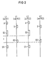
- the individual data records are transferred to the buffer memory PS already mentioned in the order in which they were created. This buffer memory is continuously checked for the presence of stored data records. If there is at least one such data record in the buffer memory, the data switching system EDS in turn transmits a request signal A (FIG. 2) via the dedicated lines L1 and L2 to the microprocessor arrangements PC1 and PC2 (FIG. 1) of the call data processing system under the control of the program control unit PE .
- a request signal is formed, for example, like the following also listed signals to be transmitted via the two dedicated lines, from a defined bit sequence.
- the two microprocessor arrangements PC1 and PC2 each emit a ready signal (B in FIG. 2) when they are ready to receive a data record, which may be present here for both.
- the data record to be transmitted next is copied in the data switching system EDS in the buffer memory PS and transmitted to the two microprocessor arrangements. (DS in FIG 2).
- the data record may contain security information, for example in the form of test marks, which permit such a check.
- Various methods for checking transmitted data signals based on backup information are already known, so that there is no need to go into them here. Examples of this are just security procedures using parity bits or block security procedures.
- the relevant data record is stored by them in the associated memory arrangement MP1 or PM2.
- Each of the two microprocessor arrangements then issues an acknowledgment signal (EQ1 in FIG. 2) to the data switching system via the associated dedicated line.
- the result of the aforementioned check of the received data record results from these acknowledgment signals.
- the data exchange system EDS concludes the transmission process by emitting a control signal ST1 (FIG. 2) to both microprocessor arrangements.
- This control signal indicates that the data record for further processing was received without errors in the two microprocessor arrangements.
- this control signal is emitted, the data record previously stored in the buffer memory PS of the data switching system is deleted.
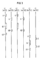
- FIG. 3 shows the case in which a data record transmitted by the data exchange system EDS could only be received without error by one of the microprocessor arrangements.
- This may be the microprocessor arrangement PC1, for example.
- This acknowledges receipt of the data record in the manner described above by issuing an acknowledgment signal EQ1 (positive acknowledgment signal).
- the microprocessor arrangement PC2 on the other hand, emits an acknowledgment signal EQ2, which indicates faulty reception (negative acknowledgment signal).
- the data switching system EDS now only outputs a control signal ST2 to the microprocessor arrangement from which the positive acknowledgment signal was previously received. In the present example, this is the microprocessor arrangement PC1.
- the control signal ST2 just mentioned tells the microprocessor arrangement PC1 that only the transmitted data record has been received without errors.
- the microprocessor arrangement PC1 now copies the data record previously received from it and stored in the memory arrangement MP1 and transmits this copied data record to the microprocessor arrangement PC2, which accepts this data record in the memory arrangement MP2.
- the aforementioned connection line L3 (FIG. 1) is used for this transmission, which takes place without the involvement of the data switching system EDS. Signals, for example, can be exchanged via this connection line between the two microprocessing arrangements for the signals explained above used for the delivery of a data record from the data switching system, as indicated in FIG. 3. After this transfer has been completed, the data record previously output by the data switching system is then available in the two memory arrangements MP1 and MP2 (FIG2) for further processing.
- the two microprocessor arrangements each have a floppy disk drive
- the data record to be transmitted is first transferred to a floppy disk by entering the aforementioned transmission command in the microprocessor arrangement PC1.
- the floppy disk contents can then be transferred to the memory array MP2 after the relevant diskettes have been inserted into the diskette drive of the microprocessor arrangement PC2.
- the counter arrangement Z shown in FIG. 1 can be used, for example, which may have two separate counter devices assigned to the microprocessor arrangements and controlled by a clock generator.
- these counting devices are each transferred from an initial state to a counting state in which they each count from an initial counter reading to a predetermined final counter reading. This final count determines the maximum time for the receipt of the acknowledgment signal.
Abstract
Description
Die Erfindung betrifft ein Verfahren zum Übertragen von über eine Fernmeldevermittlungsanlage, insbesondere eine Datenvermittlungsanlage, verlaufende Verbindungen betreffenden Informationen, welche in der Fernmeldevermittlungsanlage verbindungsindividuell ermittelt und in verbindungsindividuellen Datensätzen in einem Zwischenspeicher zwischengespeichert werden, zu einer mit der Fernmeldevermittlungsanlage verbundenen Informationsverarbeitungsanlage.The invention relates to a method for transmitting information relating to connections via a telecommunications switching system, in particular a data switching system, which is determined in the telecommunications switching system for each connection and temporarily stored in connection-specific data records in a buffer, to an information processing system connected to the telecommunications switching system.
Es ist bereits bekannt (Der Dienst bei der Deutschen Bundespost, Teilband 4, Datenvermittlungstechnik (EDS), R.v. Decker's Verlag G. Schenk, Heidelberg, Hamburg 1987, Seiten 232 bis 242), in einer Datenvermittlungsanlage für jede der über diese verlaufenden Verbindungen sogenannte Rufdaten zu ermitteln und zwischenzuspeichern. Diese Rufdaten dienen beispielsweise für eine Gebührenermittlung für die einzelnen Verbindungen bzw. für eine Verkehrswerterfassung. Für die Ermittlung der Rufdaten wird bei jedem Verbindungsaufbau ein sogenannter Anfangssatz erstellt, in welchem u. a. neben einer Kennung für den die jeweilige Verbindung wünschenden Teilnehmer (rufender Teilnehmer) die den gewünschten Teilnehmer (gerufener Teilnehmer) bezeichnenden Wahlinformationen und Angaben bezüglich des Zeitpunktes des Beginns der Gebührenpflicht sowie der Art der Gebührenberechnung gespeichert sind. Bei Abbau der jeweiligen Verbindung wird dann ein weiterer sogenannter Endesatz erstellt, welcher beispielsweise neben der Kennung für den rufenden Teilnehmer Angaben bezüglich des Endzeitpunktes der Gebührenpflicht enthält.It is already known (the service at the Deutsche Bundespost, Sub-Volume 4, Data Transfer Technology (EDS), Rv Decker's Verlag G. Schenk, Heidelberg, Hamburg 1987, pages 232 to 242), in a data exchange system for each of the connections running over these connections, so-called call data to determine and cache. These call data are used, for example, to determine the charges for the individual connections or to record the market value. To determine the call data, a so-called initial sentence is created each time a connection is established, in which u. a. In addition to an identifier for the subscriber (calling subscriber) wishing the respective connection, the dialing information designating the desired subscriber (called subscriber) and information regarding the point in time at which the obligation to pay charges begins and the type of charge calculation are stored. When the respective connection is cleared down, a further so-called end sentence is then created, which contains, for example, in addition to the identifier for the calling subscriber, information relating to the end time of the fee obligation.
Anfangs- und Endesätze werden dabei jeweils getrennt in einen Ausgangspuffer übertragen und verbleiben dort bis dieser vollständig gefüllt ist. Ist dieser Zustand des Ausgangspuffers erreicht, werden die darin gespeicherten Anfangs- und Endesätze in einen Plattenspeicher der Datenvermittlungsanlage übernommen. Für eine spätere Verarbeitung der in diesem Plattenspeicher in Form von Anfangs- und Endesätzen gespeicherten Rufdaten werden diese zu einem Rufdatenrechner übertragen. Für diese Übertragung ist eine nicht näher erläuterte Datenübertragungsprozedur vorgesehen.Start and end sentences are separated into one Transfer the output buffer and remain there until it is completely filled. When this state of the output buffer has been reached, the start and end blocks stored therein are transferred to a disk memory of the data switching system. For later processing of the call data stored in this disk memory in the form of start and end records, these are transmitted to a call data computer. A data transmission procedure (not explained in more detail) is provided for this transmission.
Darüber hinaus ist es bereits bekannt (Heidelberger Taschenbücher, Datenfernverarbeitung, H. Hofer, Springer-Verlag, Berlin, Heidelberg, New York 1978, Seiten 128 bis 133), daß für eine Übertragung von in einer Datenstation vorliegenden Datenblöcken zu einer Außenstelle hin die Datenstation zunächst ein Anforderungssignal an die Außenstelle abgibt. Die Außenstelle antwortet, falls sie zur Datenaufnahme bereit ist, mit einer positiven Rückmeldung. Auf diese Rückmeldung hin erfolgt die Übertragung eines Datenblockes. Der Empfang dieses Datenblockes wird von der Außenstelle her durch Abgabe eines Quittungssignals, welches Aufschluß über den Empfang des Datenblockes gibt, bestätigt.In addition, it is already known (Heidelberger Taschenbuch, Datenfernverarbeitung, H. Hofer, Springer-Verlag, Berlin, Heidelberg, New York 1978, pages 128 to 133) that the data station is used for the transmission of data blocks present in a data station to a branch office first sends a request signal to the branch office. The branch office replies with a positive response if it is ready for data acquisition. A data block is transmitted in response to this feedback. The reception of this data block is confirmed by the branch office by issuing an acknowledgment signal which provides information about the reception of the data block.
Es ist nun Aufgabe der vorliegenden Erfindung, einen Weg zu zeigen, wie ein Verfahren der eingangs genannten Art ausgebildet werden kann, um mit einem geringen Steuerungsaufwand in der Fernmeldevermittlungsanlage eine sichere Übertragung von in dieser vorliegenden, Verbindungen betreffende Informationen zu einer Informationsverarbeitungsanlage hin zu ermöglichen.It is an object of the present invention to show a way in which a method of the type mentioned at the outset can be designed in order to enable secure transmission of information relating to connections to an information processing system in the telecommunication switching system with little control effort.
Gelöst wird die vorstehend aufgezeigte Aufgabe bei einem Verfahren der eingangs genannten Art durch die im kennzeichnenden Teil des Patentanspruches 1 angegebenen Verfahrensmerkmale.The object outlined above is achieved in a method of the type mentioned at the outset by the method features specified in the characterizing part of patent claim 1.
Die Erfindung bringt den Vorteil mit sich, daß die in der Fernmeldevermittlungsanlage anfallenden Datensätze fortlaufend zu der Informationsverarbeitungsanlage hin übertragbar sind, so daß im Vergleich zum Stand der Technik mit einem relativ kleinen Zwischenspeicher in der Fernmeldevermittlungsanlage ausgekommen werden kann. Als Zwischenspeicher kann beispielsweise ein festgelegter Bereich des Arbeitsspeicher einer speicherprogrammierten Fernmeldevermittlungsanlage dienen. Ein weiterer Vorteil der Erfindung besteht darin, daß die Datensätze für eine spätere Verarbeitung nicht nur in der Informationsverarbeitungsanlage in voneinander unabhängigen Speicherordnungen redundant gespeichert werden, sondern daß die einzelnen Datensätze von der Fernmeldevermittlungsanlage aus über gesonderte Übertragungswege zu zwei voneinander unabhängigen Verarbeitungseinrichtungen der Informationsverarbeitungsanlage übertragen werden. Damit ist beispielsweise auch bei Ausfall eines der Übertragungswege bzw. bei Ausfall einer der Verarbeitungseinrichtungen eine Übertragung von Datensätzen zu der nicht von einem Ausfall betroffenen Verarbeitungseinrichtung möglich. Die Fernmeldevermittlungsanlage ist somit bezüglich der Verwaltung dieser Datensätze entlastet. Die übertragenen Datensätze können dann ohne Einbeziehung der Fernmeldevermittlungsanlage im Falle eines Ausfalls eines der Übertragungswege sofort, im Falle eines Ausfalls einer Verarbeitungseinrichtung nach deren Instandsetzung unter der Steuerung der nicht von einem Ausfall betroffenen Verarbeitungseinrichtung redundant gespeichert werden.The invention has the advantage that the Telecommunications switching system data records are continuously transferred to the information processing system, so that in comparison to the prior art, a relatively small buffer in the telecommunications switching system can be used. For example, a defined area of the main memory of a memory-programmed telecommunications switching system can serve as a buffer. Another advantage of the invention is that the data records for later processing are not only stored redundantly in mutually independent storage systems in the information processing system, but that the individual data records are transmitted from the telecommunication switching system via separate transmission paths to two mutually independent processing devices of the information processing system. This means, for example, that even if one of the transmission paths fails or if one of the processing devices fails, data records can be transferred to the processing device not affected by a failure. The telecommunications switching system is thus relieved of the burden on the administration of these data records. The transmitted data records can then be stored without the involvement of the telecommunications switching system in the event of a failure of one of the transmission routes immediately, in the event of a failure of a processing device after its repair under the control of the processing device not affected by a failure.
Vorteilhafte Ausgestaltungen der Erfindung ergeben sich aus den Unteransprüchen.Advantageous embodiments of the invention result from the subclaims.
Im folgenden wird nun die Erfindung anhand von Zeichnungen beispielsweise näher beschrieben.
- FIG 1 zeigt eine Datenvermittlungsanlage, in welcher das Verfahren gemäß der vorliegenden Erfindung angewandt ist, und
- FIG 2 und 3 zeigen Zeitdiagramme, auf die im Zuge der Beschreibung der Erfindung eingegangen wird.
- 1 shows a data switching system in which the method according to the present invention is applied, and
- 2 and 3 show time diagrams which will be discussed in the course of the description of the invention.
In FIG 1 ist eine Datenvermittlungsanlage EDS ausschnittweise dargestellt, welche allgemein für die Vermittlung von Datensignalen dient. Unter diese Datensignale fallen dabei beispielsweise auch Fernschreibzeichen oder Sprachsignale in digital codierter Form. Von der Datenvermittlungsanlage sind zwei verschiedene Gruppen von Anschlußschaltungen dargestellt. Zu einer ersten Gruppe gehören dabei die Anschlußschaltungen AA1 bis AAn, von denen in FIG 1 lediglich die Anschlußschaltungen AA1 und AAn angedeutet sind. Diese Anschlußschaltungen dienen dazu, digitale Datensignale, die nach einem asynchronen Übertragungsverfahren übertragen werden, zu verarbeiten. Beispielsweise sind somit an diese Anschlußschaltungen übliche Fernschreib- bzw. Telex- Teilnehmerendgeräte anschließbar. In FIG 1 sind mit der Anschlußschaltung AAn mit Tx1 bis Txm bezeichnete Telex-Teilnehmerendgeräte verbunden.FIG. 1 shows a section of a data switching system EDS, which is generally used for the switching of data signals. These data signals also include, for example, telex characters or voice signals in digitally coded form. Two different groups of connection circuits are shown of the data switching system. A first group includes the connection circuits AA1 to AAn, of which only the connection circuits AA1 and AAn are indicated in FIG. These connection circuits are used to process digital data signals which are transmitted using an asynchronous transmission method. For example, conventional telex or telex subscriber terminals can thus be connected to these connection circuits. In FIG. 1, telex subscriber terminals designated Tx1 to Txm are connected to the connection circuit AAn.
Die zweite Gruppe von Anschlußschaltungen umfaßt die Anschlußschaltungen AS1 bis ASn. Von diesen sind in FIG 1 lediglich die Anschlußschaltungen AS1 und ASn dargestellt. Diese Anschlußschaltungen verarbeiten digitale Datensignale in Form von Bitgruppen (Envelopes), die nach einem synchronen Übertragungsverfahren übertragen werden. Beispielsweise können diese Anschlußschaltungen digitale Datensignale entsprechend dem internationalen Alphabet IA Nr. 5 abgeben und aufnehmen. An diese Anschlußschaltungen sind somit beispielsweise sogenannte Bürofernschreibmaschinen anschließbar, die auch als Teletex-Teilnehmerendgeräte bezeichnet werden. In FIG 1 sind an die Anschlußschaltung ASn mit Ttx1 bis Ttxm bezeichnete Teletex-Teilnehmerendgeräte angeschlossen.The second group of connection circuits comprises the connection circuits AS1 to ASn. Of these, only the connection circuits AS1 and ASn are shown in FIG. These connection circuits process digital data signals in the form of bit groups (envelopes) which are transmitted using a synchronous transmission method. For example, these connection circuits can output and record digital data signals in accordance with international alphabet IA No. 5. So-called office teleprinters, which are also referred to as teletex subscriber terminals, can thus be connected to these connection circuits. In FIG. 1, teletex subscriber terminals designated Ttx1 to Ttxm are connected to the connection circuit ASn.
Bezüglich der zuvor genannten Anschlußschaltungen sei darauf hingewiesen, daß diese jeweils mit einer Vielzahl von Übertragungsleitungen verbunden sind, die als Teilnehmerleitungen für den Anschluß von beispielsweise Telex-Teilnehmerendgeräten bzw. Teletex-Teilnehmerendgeräten oder als Amtsverbindungsleitungen benutzbar sind, über welche beispielsweise jeweils zwei Datenvermittlungsanlagen miteinander in Verbindung stehen.With regard to the aforementioned connection circuits, it should be pointed out that they are each connected to a large number of transmission lines which act as subscriber lines for the connection of, for example, Telex subscriber terminals or Teletex subscriber terminals or as exchange lines can be used, for example, via which two data switching systems are connected to each other.
Neben den zuvor genannten Anschlußschaltungen sind als Schaltungsteile der Datenvermittlungsanlage EDS noch mit den Anschlußschaltungen verbundene Eingabe-/Ausgabe-Codewandler EACD und EACW, eine Übertragungsablaufsteuerung UEAS, eine Speichereinheit SE und schließlich eine Programmsteuereinheit PE angegeben. Auf das Zusammenwirken dieser Schaltungsteile wird hier nicht näher eingegangen, da dies bereits hinlänglich bekannt ist (siehe beispielsweise "Siemens-Zeitschrift", Heft 2, 1977, Seiten 82 bis 87).In addition to the aforementioned connection circuits, input / output code converters EACD and EACW, a transmission sequence control unit UEAS, a memory unit SE and finally a program control unit PE are also specified as circuit parts of the data switching system EDS with input / output code converters EACD and EACW connected to the connection circuits. The interaction of these circuit parts is not discussed in detail here, since this is already well known (see, for example, "Siemens Journal", Issue 2, 1977, pages 82 to 87).
Von der genannten Speichereinheit SE sind für die Erläuterung des Verfahrens gemäß der vorliegenden Erfindung lediglich ein Pufferspeicher PS und eine steuerbare Zähleranordnung Z dargestellt.From the memory unit SE mentioned, only a buffer memory PS and a controllable counter arrangement Z are shown for the explanation of the method according to the present invention.
An die genannte Anschlußschaltung AA1 ist eine Rufdatenverarbeitungsanlage RDE über zwei Übertragungsleitungen L1 und L2 angeschlossen. Diese Übertragungsleitungen sind jeweils als Standleitung benutzt. Die Rufdatenverarbeitungsanlage weist zwei voneinander unabhängige Mikroprozessoranordnungen PC1 und PC2 auf, die jeweils mit einer der gerade genannten Übertragungsleitungen in Verbindung stehen. Die Mikroprozessoranordnung PC1 möge beispielswseise mit der Übertragungsleitung L1 und die Mikroprozessoranordnung PC2 mit der Übertragungsleitung L2 verbunden sein. Diese Mikroprozessoranordnungen, die beispielsweise jeweils durch einen Personalcomputer gebildet sein mögen, weisen jeweils eine externe Speicheranordnung auf. Bei diesen Speicheranordnungen kann es sich beispielsweise um Magnetplattenspeicher handeln. In FIG 1 ist die der Mikroprozessoranordnung PC1 zugehörige Speicheranordnung mit MP1 bezeichnet. Die mit der Mikroprozessoranordnung PC2 verbundene Speicheranordnung trägt dagegen die Bezeichnung MP2.A call data processing system RDE is connected to said connection circuit AA1 via two transmission lines L1 and L2. These transmission lines are used as dedicated lines. The call data processing system has two mutually independent microprocessor arrangements PC1 and PC2, each of which is connected to one of the transmission lines just mentioned. The microprocessor arrangement PC1 may for example be connected to the transmission line L1 and the microprocessor arrangement PC2 to the transmission line L2. These microprocessor arrangements, which may each be formed by a personal computer, for example, each have an external memory arrangement. These storage arrangements can be magnetic disk storage, for example. In FIG. 1, the memory arrangement associated with the microprocessor arrangement PC1 is designated MP1. In contrast, the memory arrangement connected to the microprocessor arrangement PC2 bears the designation MP2.
Die zuvor genannten Mikroprozessoranordnungen PC1 und PC2 stehen miteinander über eine Verbindungsleitung L3 in Verbindung. Außerdem ist an jede der Mikroprozessoranordnungen eine Ausgabeeinrichtung beispielswseise in Form eines Druckers D anschließbar.The aforementioned microprocessor arrangements PC1 and PC2 are connected to one another via a connecting line L3. In addition, an output device, for example in the form of a printer D, can be connected to each of the microprocessor arrangements.
Nachdem zuvor der Aufbau der in FIG 1 dargestellten Schaltungsanordnung erläutert worden ist, wird nunmehr näher auf das Verfahren gemäß der vorliegenden Erfindung anhand der FIG 2 und 3 eingegangen.After the structure of the circuit arrangement shown in FIG. 1 has been explained above, the method according to the present invention will now be discussed in more detail with reference to FIGS. 2 and 3.
Von der Datenvermittlungsanlage EDS wird für jede der über sie verlaufenden Verbindungen unter Steuerung der Programmsteuereinheit PE ein Datensatz erstellt, der die eingangs erwähnten Informationen für eine spätere Gebührenermittlung und ggf. für eine Verkehrsstatistik enthält. Die einzelnen Datensätze werden in der Reihenfolge ihrer Erstellung in den bereits genannten Pufferspeicher PS übertragen. Dieser Pufferspeicher wird fortlaufend hinsichtlich des Vorhandenseins von gespeicherten Datensätzen überprüft. Liegt wenigstens ein solcher Datensatz in dem Pufferspeicher vor, so wird von der Datenvermittlungsanlage EDS wiederum unter der Steuerung der Programmsteuereinheit PE ein Anforderungssignal A (FIG 2) über die Standleitungen L1 und L2 zu den Mikroprozessoranordnungen PC1 und PC2 (FIG 1) der Rufdatenverarbeitungsanlage hin übertragen. Ein solches Anforderungssignal ist beispielsweise, wie auch die nachfolgenden noch aufgeführten, über die beiden Standleitungen zu übertragenden Signale, aus einer festgelegten Bitfolge gebildet.The data exchange system EDS creates a data record for each of the connections running over it under the control of the program control unit PE, which contains the information mentioned at the beginning for a later determination of fees and possibly for traffic statistics. The individual data records are transferred to the buffer memory PS already mentioned in the order in which they were created. This buffer memory is continuously checked for the presence of stored data records. If there is at least one such data record in the buffer memory, the data switching system EDS in turn transmits a request signal A (FIG. 2) via the dedicated lines L1 and L2 to the microprocessor arrangements PC1 and PC2 (FIG. 1) of the call data processing system under the control of the program control unit PE . Such a request signal is formed, for example, like the following also listed signals to be transmitted via the two dedicated lines, from a defined bit sequence.
Die beiden Mikroprozessoranordnungen PC1 und PC2 geben bei ihrer Bereitschaft für die Aufnahme eines Datensatzes, die hier für beide vorliegen möge, jeweils ein Bereitmeldungssignal (B in FIG 2) ab. Auf das Eintreffen dieser Bereitmeldungssignale hin wird in der Datenvermittlungsanlage EDS der als nächste zu übertragende Datensatz in dem Pufferspeicher PS kopiert und zu den beiden Mikroprozessoranordnungen hin übertragen. (DS in FIG 2). Diese überprüfen daraufhin den gerade empfangenen Datensatz hinsichtlich einer fehlerfreien Übertragung. Dem Datensatz mögen dafür von der Datenvermittlungsanlage her Sicherungsinformationen beispielsweise in Form von Prüfzeichen beigefügt sein, die eine derartige Überprüfung gestatten. Es sind bereits verschiedene Verfahren für die Überprüfung von übertragenen Datensignalen anhand von Sicherungsinformationen bekannt, so daß hier nicht näher darauf eingegangen werden muß. Als Beispiele seinen hier lediglich Sicherungsverfahren mit Hilfe von Paritätsbits oder Blocksicherungsverfahren genannt.The two microprocessor arrangements PC1 and PC2 each emit a ready signal (B in FIG. 2) when they are ready to receive a data record, which may be present here for both. Upon the arrival of these ready signals, the data record to be transmitted next is copied in the data switching system EDS in the buffer memory PS and transmitted to the two microprocessor arrangements. (DS in FIG 2). These then check the data record just received for error-free transmission. For this purpose, the data record may contain security information, for example in the form of test marks, which permit such a check. Various methods for checking transmitted data signals based on backup information are already known, so that there is no need to go into them here. Examples of this are just security procedures using parity bits or block security procedures.
Nach der gerade erwähnten Überprüfung des empfangenen Datensatzes in den beiden Mikroprozessoranordnungen PC1 und PC 2 wird von diesen der betreffende Datensatz in die zugehörige Speicheranordnung MP1 bzw. PM2 abgespeichert. Anschließend gibt jede der beiden Mikroprozessoranordnungen ein Quittungssignal (EQ1 in FIG 2) über die jeweils zugehörige Standleitung an die Datenvermittlungsanlage ab. Aus diesen Quittungssignalen geht jeweils das Ergebnis der zuvor genannten Überprüfung des empfangenen Datensatzes hervor (positives bzw. negatives Quittungssignal). Zeigen die Quittungssignale dabei an, daß in beiden Mikroprozessoranordnungen der übertragene Datensatz fehlerfrei empfangen worden ist, so schließt die Datenvermittlungsanlage EDS den Übertragungsvorgang mit der Abgabe eines Steuersignals ST1 (FIG 2) an beide Mikroprozessoranordnungen ab. Dieses Steuersignal zeigt an, daß in den beiden Mikroprozessoranordnungen der Datensatz für eine weitere Verarbeitung fehlerfrei empfangen worden ist. Auf die Abgabe dieses Steuersignals hin wird im übrigen der bis dahin noch im Pufferspeicher PS der Datenvermittlungsanlage gespeicherte Datensatz gelöscht.After the above-mentioned check of the received data record in the two microprocessor arrangements PC1 and PC 2, the relevant data record is stored by them in the associated memory arrangement MP1 or PM2. Each of the two microprocessor arrangements then issues an acknowledgment signal (EQ1 in FIG. 2) to the data switching system via the associated dedicated line. The result of the aforementioned check of the received data record (positive or negative acknowledgment signal) results from these acknowledgment signals. If the acknowledgment signals indicate that the transmitted data record has been received without error in both microprocessor arrangements, the data exchange system EDS concludes the transmission process by emitting a control signal ST1 (FIG. 2) to both microprocessor arrangements. This control signal indicates that the data record for further processing was received without errors in the two microprocessor arrangements. When this control signal is emitted, the data record previously stored in the buffer memory PS of the data switching system is deleted.
In FIG 3 ist nun der Fall dargestellt, daß ein von der Datenvermittlungsanlage EDS übertragener Datensatz lediglich von einer der Mikroprozessoranordnungen fehlerfrei empfangen werden konnte. Dies möge beispielsweise die Mikroprozessoranordnung PC1 sein. Diese quittiert in der zuvor beschriebenen Weise durch Abgabe eines Quittungssignals EQ1 (positives Quittungssignal) den Empfang des Datensatzes. Die Mikroprozessoranordnung PC2 gibt dagegen ein Quittungssignal EQ2 ab, welches einen fehlerhaften Empfang anzeigt (negatives Quittungssignal). Die Datenvermittlungsanlage EDS gibt auf den Empfang dieser Quittungssignale jetzt lediglich an diejenige Mikroprozessoranordnung ein Steuersignal ST2 ab, von welcher zuvor das positive Quittungssignal empfangen worden ist. Dies ist im vorliegenden Beispiel also die Mikroprozessoranordnung PC1.3 shows the case in which a data record transmitted by the data exchange system EDS could only be received without error by one of the microprocessor arrangements. This may be the microprocessor arrangement PC1, for example. This acknowledges receipt of the data record in the manner described above by issuing an acknowledgment signal EQ1 (positive acknowledgment signal). The microprocessor arrangement PC2, on the other hand, emits an acknowledgment signal EQ2, which indicates faulty reception (negative acknowledgment signal). When these acknowledgment signals are received, the data switching system EDS now only outputs a control signal ST2 to the microprocessor arrangement from which the positive acknowledgment signal was previously received. In the present example, this is the microprocessor arrangement PC1.
Durch das gerade genannte Steuersignal ST2 wird der Mikroprozessoranordnung PC1 mitgeteilt, daß lediglich von dieser der übertragene Datensatz fehlerfrei empfangen worden ist. Auf dieses Steuersignal hin kopiert nun die Mikroprozessoranordnung PC1 den zuvor von ihr empfangenen und in der Speicheranordnung MP1 gespeicherten Datensatz und überträgt diesen kopierten Datensatz zu der Mikroprozessoranordnung PC2 hin, die diesen Datensatz in die Speicheranordnung MP2 übernimmt. Für diese Übertragung, die ohne Einbeziehung der Datenvermittlungsanlage EDS erfolgt, wird die bereits genannte Verbindungsleitung L3 (FIG 1) benutzt. Dabei können beispielsweise über diese Verbindungsleitung zwischen den beiden Mikroprozessanordnungen den für die Abgabe eines Datensatzes von der Datenvermittlungsanlage her verwendeten, zuvor erläuterten Signalen entsprechende Signale ausgetauscht werden, wie es in FIG 3 angedeutet ist. Nach Abschluß dieser Übertragung steht dann der zuvor von der Datenvermittlungsanlage abgegebene Datensatz in den beiden Speicheranordnungen MP1 und MP2 (FIG2) für eine weitere Verarbeitung zur Verfügung.The control signal ST2 just mentioned tells the microprocessor arrangement PC1 that only the transmitted data record has been received without errors. In response to this control signal, the microprocessor arrangement PC1 now copies the data record previously received from it and stored in the memory arrangement MP1 and transmits this copied data record to the microprocessor arrangement PC2, which accepts this data record in the memory arrangement MP2. The aforementioned connection line L3 (FIG. 1) is used for this transmission, which takes place without the involvement of the data switching system EDS. Signals, for example, can be exchanged via this connection line between the two microprocessing arrangements for the signals explained above used for the delivery of a data record from the data switching system, as indicated in FIG. 3. After this transfer has been completed, the data record previously output by the data switching system is then available in the two memory arrangements MP1 and MP2 (FIG2) for further processing.
Abweichend von der gerade erläuterten Abgabe eines Datensatzes von der Mikroprozessoranordnung PC1 aus kann auch so vorgegangen sein, daß auf den Empfang des Steuersignals ST2 hin zunächst lediglich der gerade empfangene Datensatz in der Speicheranordnung MP1 als ein zu übertragender Datensatz markiert wird und daß diese Speicheranordnung durch Eingabe eines Bedienkommandos hinsichtlich des Vorliegens eines solchen Datensatzes abfragbar ist.
Bei Vorliegen eines solchen Datensatzes kann dann beispielsweise durch Eingabe eines Übertragungskommandos eine Übertragung in der zuvor erläuterten Weise über die Verbindungsleitung L3 (FIG 3) erfolgen. Für den Fall, daß die beiden Mikroprozessoranordnungen jeweils über ein Disketten-Laufwerk verfügen, besteht eine weitere Möglichkeit darin, daß durch Eingabe des zuvor genannten Übertragungskommandos in der Mikroprozessoranordnung PC1 der zu übertragende Datensatz zunächst auf eine Diskette übernommen wird. Der Disketteninhalt kann dann nach Einsetzen der betreffenden Disketten in das Disketten-Laufwerk der Mikroprozessoranordnung PC2 in die Speicheranordnung MP2 übernommen werden.Deviating from the delivery of a data set from the microprocessor arrangement PC1 just explained, it can also be done that, upon receipt of the control signal ST2, only the data set just received is first marked in the memory arrangement MP1 as a data set to be transmitted and that this memory arrangement can be queried by entering an operating command with regard to the presence of such a data record.
If such a data record is available, a transmission can then take place via the connecting line L3 (FIG. 3), for example by entering a transmission command. In the event that the two microprocessor arrangements each have a floppy disk drive, there is a further possibility that the data record to be transmitted is first transferred to a floppy disk by entering the aforementioned transmission command in the microprocessor arrangement PC1. The floppy disk contents can then be transferred to the memory array MP2 after the relevant diskettes have been inserted into the diskette drive of the microprocessor arrangement PC2.
Bezüglich der Übertragung eines Datensatzes von der Datenvermittlungsanlage EDS her sei noch darauf hingewiesen, daß das Eintreffen der von den beiden Mikroprozessoranordnungen PC1 und PC2 abgegebenen Quittungssignale (EQ1 bzw. EQ2) zeitlich überwacht wird. Dazu ist beispielsweise die in FIG 1 dargestellte Zähleranordnung Z benutzbar, die zwei gesonderte, den Mikroprozessoranordnungen zugeordnete, durch einen Taktgenerator gesteuerte Zähleinrichtungen aufweisen möge. Bei Abgabe eines Datensatzes an die Mikroprozessoranordnungen PC1 und PC2 werden diese Zähleinrichtungen jeweils von einem Anfangszustand in einen Zählzustand überführt, in welchem sie jeweils von einem Anfangszählerstand aus bis zu einem vorgegebenen Endzählerstand zählen. Dieser Endzählerstand legt die maximale Zeitspanne für das Eintreffen des Quittungssignals fest. Tritt ein Quittungsssignal vor Erreichen dieses Endzählerstandes ein, so wird die in Frage kommende Zähleinrichtung vorzeitig wieder in ihren Anfangszustand überführt. Anderenfalls wird bei Erreichen des Endzählerstandes von der jeweiligen Zähleinrichtung ein Signal abgegeben, welches von der Datenvermittlungsanlage EDS als Quittungssignal für einen fehlerhaft empfangenen Datensatz bewertet wird. Damit laufen dann bei Auftreten eines solchen Signals die bereits anhand der FIG 3 erläuterten Übertragungsvorgänge ab.With regard to the transmission of a data record from the data exchange system EDS, it should also be pointed out that the arrival of the acknowledgment signals (EQ1 and EQ2) emitted by the two microprocessor arrangements PC1 and PC2 is monitored over time. For this purpose, the counter arrangement Z shown in FIG. 1 can be used, for example, which may have two separate counter devices assigned to the microprocessor arrangements and controlled by a clock generator. When a data record is delivered to the microprocessor arrangements PC1 and PC2, these counting devices are each transferred from an initial state to a counting state in which they each count from an initial counter reading to a predetermined final counter reading. This final count determines the maximum time for the receipt of the acknowledgment signal. If an acknowledgment signal occurs before this final counter reading is reached, the counting device in question is returned to its initial state prematurely. Otherwise, when the final counter reading is reached, a signal is emitted by the respective counting device, which is evaluated by the data switching system EDS as an acknowledgment signal for an incorrectly received data record. Thus, when such a signal occurs, the ones already explained with reference to FIG. 3 run Transfers from.
Abschließend sei noch darauf hingewiesen, daß zwar vorstehend das Verfahren gemäß der vorliegenden Erfindung am Beispiel einer Datenvermittlungsanlage erläutert worden ist. Dieses Verfahren ist aber nicht nur auf derartige Anlagen beschränkt, sondern kann allgemein für Fernmeldevermittlungsanlagen benutzt werden, welche für die einzelnen Verbindungen ermittelte Informationen beispielsweise für eine Gebührenermittlung zu einer externen Informationsverarbeitungsanlage hin übertragen.Finally, it should be pointed out that the method according to the present invention has been explained above using the example of a data exchange system. However, this method is not only limited to such systems, but can generally be used for telecommunications switching systems which transmit information determined for the individual connections to an external information processing system, for example for determining charges.
Claims (5)
dadurch gekennzeichnet,
daß der Zwischenspeicher fortlaufend auf das Vorhandensein von Datensätzen überprüft wird,
daß bei Vorliegen mindestens eines Datensatzes in dem Zwischenspeicher von der Fernmeldevermittlungsanlage her ein Anforderungssignal an zwei gesonderte, der Informationsverarbeitungsanlage zugehörige Verarbeitungseinrichtungen (PC1, PC2), welche jeweils über eine gesonderte Leitungsanordnung mit der Fernmeldevermittlungsanlage verbunden sind, übertragen wird,
daß von den Verarbeitungseinrichtungen (PC1,PC2) auf ein derartiges Anforderungssignal hin bei deren Bereitschaft zur Aufnahme eines Datensatzes jeweils ein Bereitmeldungssignal abgegeben wird, daß bei Eintreffen wenigstens eines Bereitmeldungssignals von der Fernmeldevermittlungsanlage (EDS) der als nächster zu übertragende Datensatz zu der jeweiligen Verarbeitungseinrichtung bzw. den Verarbeitungseinrichtungen übertragen wird, der in dieser bzw. diesen hinsichtlich einer fehlerfreien Übertragung überprüft und in eine der jeweiligen Verarbeitungseinrichtung zugeordnete Speicheranordnung (MP1 bzw. MP2) übernommen wird,
daß von der jeweiligen Verarbeitungseinrichtung bzw. den Verarbeitungseinrichtungen daraufhin ein den Empfang des gerade übernommenen Datensatzes betreffendes Quittungssignal abgegeben wird,
daß von der Fernmeldevermittlungsanlage bei Eintreffen lediglich eines einen fehlerfreien Empfang anzeigenden Quittungssignals ein Steuersignal an diejenige Verarbeitungseinrichtung (z. B. PC1) abgegeben wird, von der zuvor der Datensatz fehlerfrei empfangen worden ist,
und daß auf ein derartiges Steuersignal hin der in der betreffenden Verarbeitungseinrichtung fehlerfrei empfangene, in der zugehörigen Speicheranordnung gespeicherte Datensatz zusätzlich in die Speicheranordnung der anderen Verarbeitungseinrichtung (PC2) übertragen wird.1.Method for transmitting information relating to connections via a telecommunications switching system (EDS), in particular a data switching system, which is determined in the telecommunications switching system for each connection and temporarily stored in connection-specific data records in a buffer (PS), to an information processing system (RDE) connected to the telecommunications switching system ), each of which is connected to the telecommunications switching system via a separate line arrangement,
characterized by
that the buffer is continuously checked for the presence of data records,
that if there is at least one data record in the buffer from the telecommunications switching system, a request signal is transmitted to two separate processing devices (PC1, PC2) associated with the information processing system, each of which is connected to the telecommunications switching system via a separate line arrangement,
that the processing devices (PC1, PC2), in response to such a request signal when they are ready to receive a data record, emit a ready signal that when at least one ready signal arrives from the telecommunications switching system (EDS), the data record to be transmitted next to the respective processing device or is transmitted to the processing devices, which is checked in this or these for error-free transmission and is transferred to a memory arrangement (MP1 or MP2) assigned to the respective processing device,
that the respective processing device or the processing devices then issues an acknowledgment signal relating to the reception of the data record just received,
that from the telecommunications switching system only a receipt signal indicating an error-free reception upon arrival a control signal is sent to that processing device (e.g. PC1) from which the data record was previously received without errors,
and that, in response to such a control signal, the data record received without error in the processing device concerned and stored in the associated storage arrangement is additionally transmitted to the storage arrangement of the other processing device (PC2).
dadurch gekennzeichnet,
daß bei Eintreffen eines einen fehlerhaften Empfang eines Datensatzes anzeigenden Quittungssignals der betreffende Datensatz zumindest ein weiteres Mal zu der jeweiligen Verarbeitungseinrichtung (z. B. PC2) hin übertragen wird
und daß erst nach Auswerten des daraufhin von der jeweiligen Verarbeitungseinrichtung abgegebenen Quittungssignals in der Fernmeldevermittlungsanlage ggf. das genannte Steuersignal zu der anderen Verarbeitungseinrichtung hin (PC1) übertragen wird.2. The method according to claim 1,
characterized by
that when an acknowledgment signal indicating an incorrect receipt of a data record arrives, the data record in question is transmitted to the respective processing device (eg PC2) at least one more time
and that only after evaluation of the acknowledgment signal subsequently emitted by the respective processing device in the telecommunications switching system, if appropriate, the said control signal is transmitted to the other processing device (PC1).
dadurch gekennzeichnet,
daß auf eine Übertragung eines Datensatzes hin in einer Zeitüberwachungseinrichtung (Z) der Fernmeldevermittlungsanlage das Eintreffen von Quittungssignalen für die beiden Verarbeitungseinrichtungen gesondert zeitltich überwacht wird
und daß ein vor dem Auftreten eines Quittungssignals den Ablauf einer maximal vorgegebenen Zeitspanne anzeigendes, von der Zeitüberwachungseinrichtung abgegebenes Signal als Quittungssignal für einen fehlerhaft empfangenen Datensatz bewertet wird.3. The method according to claim 1 or 2,
characterized by
that upon receipt of a data record in a time monitoring device (Z) of the telecommunications switching system, the arrival of acknowledgment signals for the two processing devices is monitored separately in a timely manner
and that a signal indicating the expiry of a maximum predetermined period of time, which is issued by the time monitoring device, is evaluated as an acknowledgment signal for an incorrectly received data record before the occurrence of an acknowledgment signal.
dadurch gekennzeichnet,
daß auf den Empfang eines Steuersignals durch eine der Verarbeitungseinrichtungen der von dieser zuvor empfangene und in der zugehörigen Speicheranordnung gespeicherte Datensatz sofort in die Speicheranordnung der anderen Verarbeitungseinrichtung übertragen wird.4. The method according to any one of claims 1 to 3,
characterized by
that immediately upon receipt of a control signal by one of the processing devices, the data record previously received by it and stored in the associated memory arrangement in the memory arrangement is transferred to the other processing device.
dadurch gekennzeichnet,
daß auf den Empfang eines Steuersignals durch eine der Verarbeitungseinrichtungen der von dieser zuvor empfangene und in der zugehörigen Speicheranordnung gespeicherte Datensatz für eine spätere Übertragung gekennzeichnet wird.5. The method according to any one of claims 1 to 3,
characterized by
that when a control signal is received by one of the processing devices, the data record previously received by it and stored in the associated memory arrangement is identified for later transmission.
Applications Claiming Priority (2)
| Application Number | Priority Date | Filing Date | Title |
|---|---|---|---|
| DE3730106 | 1987-09-08 | ||
| DE3730106 | 1987-09-08 |
Publications (2)
| Publication Number | Publication Date |
|---|---|
| EP0306736A2 true EP0306736A2 (en) | 1989-03-15 |
| EP0306736A3 EP0306736A3 (en) | 1991-12-18 |
Family
ID=6335510
Family Applications (1)
| Application Number | Title | Priority Date | Filing Date |
|---|---|---|---|
| EP19880113282 Ceased EP0306736A3 (en) | 1987-09-08 | 1988-08-16 | Method for the transmission of connection information stored in a telecommunication exchange to an information-processing installation |
Country Status (3)
| Country | Link |
|---|---|
| US (1) | US5003460A (en) |
| EP (1) | EP0306736A3 (en) |
| ZA (1) | ZA886610B (en) |
Cited By (2)
| Publication number | Priority date | Publication date | Assignee | Title |
|---|---|---|---|---|
| DE3912078A1 (en) * | 1989-04-13 | 1990-10-18 | Telefonbau & Normalzeit Gmbh | DIGITAL TELECOMMUNICATION SYSTEM |
| DE4028997A1 (en) * | 1990-09-13 | 1992-03-19 | Telefonbau & Normalzeit Gmbh | Traffic data acquisition for telephone communication exchange - using counter memory in each de-central and central control, and address device to acquire addresses and control criteria |
Families Citing this family (4)
| Publication number | Priority date | Publication date | Assignee | Title |
|---|---|---|---|---|
| US5742848A (en) * | 1993-11-16 | 1998-04-21 | Microsoft Corp. | System for passing messages between source object and target object utilizing generic code in source object to invoke any member function of target object by executing the same instructions |
| US7827282B2 (en) * | 2003-01-08 | 2010-11-02 | At&T Intellectual Property I, L.P. | System and method for processing hardware or service usage data |
| US7080060B2 (en) * | 2003-01-08 | 2006-07-18 | Sbc Properties, L.P. | System and method for intelligent data caching |
| US7660286B2 (en) * | 2006-02-03 | 2010-02-09 | Broadcom Corporation | Jitter management for packet data network backhaul of call data |
Citations (3)
| Publication number | Priority date | Publication date | Assignee | Title |
|---|---|---|---|---|
| WO1982002784A1 (en) * | 1981-01-30 | 1982-08-19 | Telefon Ab L M Ericsson | Data communications network |
| EP0141245A2 (en) * | 1983-09-26 | 1985-05-15 | Siemens Aktiengesellschaft | Method for the operation of a couple of memory blocks normally working in parallel |
| US4646300A (en) * | 1983-11-14 | 1987-02-24 | Tandem Computers Incorporated | Communications method |
Family Cites Families (2)
| Publication number | Priority date | Publication date | Assignee | Title |
|---|---|---|---|---|
| IT1126475B (en) * | 1979-12-03 | 1986-05-21 | Honeywell Inf Systems | COMMUNICATION APPARATUS BETWEEN MORE PROCESSORS |
| FR2477809B1 (en) * | 1980-03-10 | 1987-08-21 | Jeumont Schneider | SYSTEM FOR FAST TRANSMISSION OF MESSAGES BETWEEN COMPUTERS |
-
1988
- 1988-08-16 EP EP19880113282 patent/EP0306736A3/en not_active Ceased
- 1988-08-31 US US07/238,700 patent/US5003460A/en not_active Expired - Fee Related
- 1988-09-06 ZA ZA886610A patent/ZA886610B/en unknown
Patent Citations (3)
| Publication number | Priority date | Publication date | Assignee | Title |
|---|---|---|---|---|
| WO1982002784A1 (en) * | 1981-01-30 | 1982-08-19 | Telefon Ab L M Ericsson | Data communications network |
| EP0141245A2 (en) * | 1983-09-26 | 1985-05-15 | Siemens Aktiengesellschaft | Method for the operation of a couple of memory blocks normally working in parallel |
| US4646300A (en) * | 1983-11-14 | 1987-02-24 | Tandem Computers Incorporated | Communications method |
Non-Patent Citations (4)
| Title |
|---|
| ELEKTROTECHNISCHE ZEITSCHRIFT - ETZ. Bd. 106, Nr. 16, August 1985, BERLIN DE Seiten 838 - 845; M. FINKBEINER ET AL.: 'Rechnernetz im Netzleitsystem der UZL' * |
| G. SCHENCK "Datenvermittlungstechnik (EDS)" 1978, R.V. DECKER'VERLAG, SEITEN 232 BIS 242 ,HEIDELBERG- HAMBURG, DE * |
| H. HAFER 'Datenfernverarbeitung', 1978, HEIDELBERGER TASCHENBUECHER, SEITEN 128-133, BERLIN, DE * |
| IBM TECHNICAL DISCLOSURE BULLETIN. Bd. 6, Nr. 7, 1963, NEW YORK US Seiten 90 - 91; C.V. MCNEIL: 'Self-Correcting Duplex Memory'. * |
Cited By (2)
| Publication number | Priority date | Publication date | Assignee | Title |
|---|---|---|---|---|
| DE3912078A1 (en) * | 1989-04-13 | 1990-10-18 | Telefonbau & Normalzeit Gmbh | DIGITAL TELECOMMUNICATION SYSTEM |
| DE4028997A1 (en) * | 1990-09-13 | 1992-03-19 | Telefonbau & Normalzeit Gmbh | Traffic data acquisition for telephone communication exchange - using counter memory in each de-central and central control, and address device to acquire addresses and control criteria |
Also Published As
| Publication number | Publication date |
|---|---|
| ZA886610B (en) | 1989-04-26 |
| US5003460A (en) | 1991-03-26 |
| EP0306736A3 (en) | 1991-12-18 |
Similar Documents
| Publication | Publication Date | Title |
|---|---|---|
| DE3136128C2 (en) | ||
| DE2350371C3 (en) | Method and device for testing and maintenance of data processing systems by means of spatially distant maintenance stations | |
| EP0658257B1 (en) | Communications control unit and information transmission process | |
| DE4221841C2 (en) | Monitoring control system for monitoring several monitored devices | |
| DE19831720A1 (en) | Method for determining a uniform global view of the system status of a distributed computer network | |
| DE102019130756A1 (en) | Control unit diagnostic apparatus and method thereof | |
| DE3639609A1 (en) | DEVICE FOR CHECKING DATA TRANSFER ERRORS, ESPECIALLY AT ELECTRONIC CASH REGISTERS | |
| EP0306736A2 (en) | Method for the transmission of connection information stored in a telecommunication exchange to an information-processing installation | |
| DE2903646B2 (en) | Circuit arrangement for controlling data stations in data transmission systems | |
| EP0182134B1 (en) | Method for operating a fail-safe multi-computer system with some not fail-safe input/output units | |
| DE69830231T2 (en) | CONTROL PROCEDURE FOR COMMUNICATION UNIT AND AFTER WORKING ARRANGEMENT | |
| DE3136586C2 (en) | ||
| DE3616556C2 (en) | CIRCUIT ARRANGEMENT FOR DETERMINING THE SYNCHRONOUS STATE OF A DATA TRANSMISSION SYSTEM | |
| DE3003340A1 (en) | METHOD AND CIRCUIT ARRANGEMENT FOR TRANSMITTING BINARY SIGNALS BETWEEN CONNECTING DEVICES CONNECTED TO A CENTRAL BUS LINE SYSTEM | |
| EP1221245B1 (en) | System, evaluation device and method for verifying connection-related communication data determined by a digital exchange | |
| EP0214475B1 (en) | Circuit arrangement for the transmission of data signals between control devices interconnected by a loop system | |
| EP1680895B1 (en) | Unit of the transmission of data in a serial bidirectional bus | |
| DE69815335T2 (en) | Method for detecting errors on a serial connection of an integrated circuit and device for carrying out the method | |
| DE3346806A1 (en) | Method and circuit arrangement for transmitting data signals | |
| DE3605359C2 (en) | Computer system with several computers | |
| EP0392245B1 (en) | Automatic addressing of monitoring and/or control processing units comprised in a digital information transmission system | |
| DE19837216C2 (en) | Troubleshooting in a switching center of a communication system | |
| DE2325691C3 (en) | Computerized telephone switching system | |
| DE2339008A1 (en) | FACILITY FOR DATA TRANSFER AND DATA BACKUP IN MULTIPLE TIME MEDIATION NETWORKS | |
| DE1932614C3 (en) | Test device for determining a multiple selection of processing units in a data processing system |
Legal Events
| Date | Code | Title | Description |
|---|---|---|---|
| PUAI | Public reference made under article 153(3) epc to a published international application that has entered the european phase |
Free format text: ORIGINAL CODE: 0009012 |
|
| AK | Designated contracting states |
Kind code of ref document: A2 Designated state(s): AT BE DE FR IT SE |
|
| 17P | Request for examination filed |
Effective date: 19901205 |
|
| PUAL | Search report despatched |
Free format text: ORIGINAL CODE: 0009013 |
|
| AK | Designated contracting states |
Kind code of ref document: A3 Designated state(s): AT BE DE FR IT SE |
|
| 17Q | First examination report despatched |
Effective date: 19930908 |
|
| RHK1 | Main classification (correction) |
Ipc: H04L 11/00 |
|
| STAA | Information on the status of an ep patent application or granted ep patent |
Free format text: STATUS: THE APPLICATION HAS BEEN REFUSED |
|
| 18R | Application refused |
Effective date: 19940227 |