EP0303975A2 - An arrangement for connecting a hybrid circuit to a mother board - Google Patents
An arrangement for connecting a hybrid circuit to a mother board Download PDFInfo
- Publication number
- EP0303975A2 EP0303975A2 EP88113079A EP88113079A EP0303975A2 EP 0303975 A2 EP0303975 A2 EP 0303975A2 EP 88113079 A EP88113079 A EP 88113079A EP 88113079 A EP88113079 A EP 88113079A EP 0303975 A2 EP0303975 A2 EP 0303975A2
- Authority
- EP
- European Patent Office
- Prior art keywords
- board
- printed circuit
- foils
- legs
- circuit board
- Prior art date
- Legal status (The legal status is an assumption and is not a legal conclusion. Google has not performed a legal analysis and makes no representation as to the accuracy of the status listed.)
- Granted
Links
Images
Classifications
-
- H—ELECTRICITY
- H05—ELECTRIC TECHNIQUES NOT OTHERWISE PROVIDED FOR
- H05K—PRINTED CIRCUITS; CASINGS OR CONSTRUCTIONAL DETAILS OF ELECTRIC APPARATUS; MANUFACTURE OF ASSEMBLAGES OF ELECTRICAL COMPONENTS
- H05K3/00—Apparatus or processes for manufacturing printed circuits
- H05K3/36—Assembling printed circuits with other printed circuits
- H05K3/366—Assembling printed circuits with other printed circuits substantially perpendicularly to each other
-
- H—ELECTRICITY
- H01—ELECTRIC ELEMENTS
- H01R—ELECTRICALLY-CONDUCTIVE CONNECTIONS; STRUCTURAL ASSOCIATIONS OF A PLURALITY OF MUTUALLY-INSULATED ELECTRICAL CONNECTING ELEMENTS; COUPLING DEVICES; CURRENT COLLECTORS
- H01R12/00—Structural associations of a plurality of mutually-insulated electrical connecting elements, specially adapted for printed circuits, e.g. printed circuit boards [PCB], flat or ribbon cables, or like generally planar structures, e.g. terminal strips, terminal blocks; Coupling devices specially adapted for printed circuits, flat or ribbon cables, or like generally planar structures; Terminals specially adapted for contact with, or insertion into, printed circuits, flat or ribbon cables, or like generally planar structures
- H01R12/50—Fixed connections
- H01R12/51—Fixed connections for rigid printed circuits or like structures
- H01R12/52—Fixed connections for rigid printed circuits or like structures connecting to other rigid printed circuits or like structures
-
- H—ELECTRICITY
- H05—ELECTRIC TECHNIQUES NOT OTHERWISE PROVIDED FOR
- H05K—PRINTED CIRCUITS; CASINGS OR CONSTRUCTIONAL DETAILS OF ELECTRIC APPARATUS; MANUFACTURE OF ASSEMBLAGES OF ELECTRICAL COMPONENTS
- H05K1/00—Printed circuits
- H05K1/02—Details
- H05K1/0213—Electrical arrangements not otherwise provided for
- H05K1/0216—Reduction of cross-talk, noise or electromagnetic interference
- H05K1/0218—Reduction of cross-talk, noise or electromagnetic interference by printed shielding conductors, ground planes or power plane
-
- H—ELECTRICITY
- H05—ELECTRIC TECHNIQUES NOT OTHERWISE PROVIDED FOR
- H05K—PRINTED CIRCUITS; CASINGS OR CONSTRUCTIONAL DETAILS OF ELECTRIC APPARATUS; MANUFACTURE OF ASSEMBLAGES OF ELECTRICAL COMPONENTS
- H05K2201/00—Indexing scheme relating to printed circuits covered by H05K1/00
- H05K2201/04—Assemblies of printed circuits
- H05K2201/048—Second PCB mounted on first PCB by inserting in window or holes of the first PCB
-
- H—ELECTRICITY
- H05—ELECTRIC TECHNIQUES NOT OTHERWISE PROVIDED FOR
- H05K—PRINTED CIRCUITS; CASINGS OR CONSTRUCTIONAL DETAILS OF ELECTRIC APPARATUS; MANUFACTURE OF ASSEMBLAGES OF ELECTRICAL COMPONENTS
- H05K2201/00—Indexing scheme relating to printed circuits covered by H05K1/00
- H05K2201/09—Shape and layout
- H05K2201/09145—Edge details
- H05K2201/09172—Notches between edge pads
Landscapes
- Engineering & Computer Science (AREA)
- Manufacturing & Machinery (AREA)
- Microelectronics & Electronic Packaging (AREA)
- Combinations Of Printed Boards (AREA)
- Multi-Conductor Connections (AREA)
- Shielding Devices Or Components To Electric Or Magnetic Fields (AREA)
- Structure Of Printed Boards (AREA)
- Coupling Device And Connection With Printed Circuit (AREA)
Abstract
Description
- The present invention relates to an arrangement for connecting a hybrid circuit to a mother board, the hybrid circuit comprising a printed circuit board with foils on both sides, components fixed to the printed circuit board, and printed circuit board legs by means of which the printed hybrid circuit board is connected to the mother board.
- It is previously known to fix to a printed hybrid circuit board various legs made of a well conductive material, which are connected to the components in the hybrid circuit via conductor strips of the printed circuit board and mate with apertures correspondingly made in the mother board. Such legs may be separate, or they may consist of one mechanical entity which has at predetermined intervals contact pins and is mechanically fixed to the edge of the printed circuit board. Such a structure tends to be mechanically weak, or it is space-consuming and costly if it is made sturdy enough. It is also not optimal in terms of freedom from interference, since the joints between the conductor foils and the legs form electric discontinuity points.
- The object of the present invention is to provide between a hybrid circuit and a mother board a connection which is maximally easy to manufacture, sturdy, and electrically interference-free. To achieve this, the invention is characterized in that the legs of the printed circuit board consist of projections in the board itself and that the mother board has apertures corresponding to the legs, the apertures being not copper-plated throughout, the earth foils and conductor foils in the projections being con nected to the foils of the mother board at the edges of the apertures.
- The projections are preferably formed in the edge of the printed circuit board by grinding and/or drilling, whereby the roots of the legs will be rounded. In a corresponding manner the apertures in the mother board are also made oval and rounded in such a way that two opposite parallel sides are straight over the distance of the width of the leg. The connecting of the leg of the printed circuit board to the mother board is then effected by soldering along these straight parts. Most suitably each projection has on one side an earth foil and on the other side at least one conductor foil.
- The invention is described below in greater detail in the form of an example and with reference to the accompanying drawings, in which
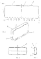
- Figure 1 depicts a diagrammatic side view of the printed circuit board itself,
- Figure 2 depicts a perspective representation of the entire hybrid circuit with its RF-shielding cover,
- Figures 3 and 4 depict the
shielding cover 5, as seen from the side, respectively as seen from the end and sectioned, and - Figures 5 and 6 depict on a larger scale how the legs of the printed circuit board engage in the mother board.
- Figure 1 thus shows diagrammatically a printed circuit board 1, which is of an insulation material and has on one side an earth foil and on the other side conductor foils, as will be described below. Furthermore, all the components of the circuit, not shown here, are fixed to the printed circuit board 1.
- Figure 2 depicts the entire hybrid circuit, which consists of the printed circuit board 1 with its components and
legs 2, and of a cover, connected to it, which has been pressed from a metal sheet and been attached by its edges to the printed circuit board 1 by, for example, soldering to its earth foil. - Figures 3 and 4 further depict only the
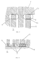
metal cover 5, as seen directly from the side of the cover and as seen from the end and sectioned. In the edge of thecover 5 there are twonotches 7 for receiving protrusions 3 of the printed circuit board 1 and two notches 8 for receivingprotrusions 4. In addition, there is a deeper continuous or two-part notch 6 through which thelegs 2 extend from the housing. - Figures 5 and 6 depict on a larger scale in detail how the
legs 2 of the hybrid circuit are connected to the mother board. The legs may be of a square cross section, as in Figure 5, or at least some of them may be rectangular, as shown in Figure 6. In themother board 12 there arecorresponding apertures 9 in which thelegs 2 fit so that those sides of the legs in which the earth foils andconductor foils 2a and 2b are located approximately coincide with the edges of theaperture 9. In terms of manufacture, it is easiest to make theapertures 9 by drilling and grinding so that their shape will be oval. - In the case presented, the foils of the mother board are located on one and the same side. The earth foil is indicated by
reference numeral 11 and the conductor foil byreference numeral 10. Theapertures 9 are not copper-plated throughout, and, when necessary, the earth foils and the conductor foils of the mother board may be situated on different sides of the mother board. It is also clear, especially if theleg 2 is especially broad, as shown on the right in Figure 6 , that there may be several conductor foils in the leg which respectively connect with several conductor foils in the mother board. The earth foils and conductor foils in thelegs 2 of the printed circuit board are connected to the earth foils and conductor foils of themother board 12 by soldering along the parallel opposite sides of theapertures 9.
Claims (5)
Applications Claiming Priority (2)
| Application Number | Priority Date | Filing Date | Title |
|---|---|---|---|
| FI873620 | 1987-08-21 | ||
| FI873620A FI84214C (en) | 1987-08-21 | 1987-08-21 | ANORDINATION FOR THE EXPLOSION OF HYBRID CRACKS BETWEEN BASPLATTA. |
Publications (3)
| Publication Number | Publication Date |
|---|---|
| EP0303975A2 true EP0303975A2 (en) | 1989-02-22 |
| EP0303975A3 EP0303975A3 (en) | 1990-07-18 |
| EP0303975B1 EP0303975B1 (en) | 1995-07-19 |
Family
ID=8524920
Family Applications (1)
| Application Number | Title | Priority Date | Filing Date |
|---|---|---|---|
| EP88113079A Expired - Lifetime EP0303975B1 (en) | 1987-08-21 | 1988-08-11 | An arrangement for connecting a hybrid circuit to a mother board |
Country Status (5)
| Country | Link |
|---|---|
| EP (1) | EP0303975B1 (en) |
| JP (1) | JPH01152686A (en) |
| DK (1) | DK168974B1 (en) |
| FI (1) | FI84214C (en) |
| NO (1) | NO883711L (en) |
Cited By (2)
| Publication number | Priority date | Publication date | Assignee | Title |
|---|---|---|---|---|
| EP0651598A1 (en) * | 1993-11-02 | 1995-05-03 | Philips Patentverwaltung GmbH | Electronic circuit module |
| EP1056319A2 (en) | 1999-05-27 | 2000-11-29 | SEW-EURODRIVE GMBH & CO. | Daughter board for insertion into a mother board |
Families Citing this family (1)
| Publication number | Priority date | Publication date | Assignee | Title |
|---|---|---|---|---|
| JPH06196833A (en) * | 1992-12-25 | 1994-07-15 | Kenwood Corp | Mounting structure of printed board |
Citations (5)
| Publication number | Priority date | Publication date | Assignee | Title |
|---|---|---|---|---|
| US4109298A (en) * | 1976-07-26 | 1978-08-22 | Texas Instruments Incorporated | Connector with printed wiring board structure |
| FR2442570A1 (en) * | 1978-11-27 | 1980-06-20 | Radiotechnique Compelec | Tracked board insertion and printed circuit board - is VIA slot enabling tracks to be soldered together |
| FR2503977A1 (en) * | 1981-04-10 | 1982-10-15 | Radiotechnique Compelec | Multiple printed circuit or hybrid circuit substrate mfg. method - allows several small circuit units to be obtained from large sheet by defining boundaries in series of holes of which walls are metallised |
| EP0089452A1 (en) * | 1982-03-18 | 1983-09-28 | Robert Bosch Gmbh | Hearing aid with amplifier circuit |
| JPS59198742A (en) * | 1983-04-25 | 1984-11-10 | Matsushita Electric Ind Co Ltd | Terminal board of integrated circuit element |
-
1987
- 1987-08-21 FI FI873620A patent/FI84214C/en not_active IP Right Cessation
-
1988
- 1988-08-11 EP EP88113079A patent/EP0303975B1/en not_active Expired - Lifetime
- 1988-08-18 DK DK464088A patent/DK168974B1/en not_active IP Right Cessation
- 1988-08-19 JP JP63204827A patent/JPH01152686A/en active Pending
- 1988-08-19 NO NO88883711A patent/NO883711L/en unknown
Patent Citations (5)
| Publication number | Priority date | Publication date | Assignee | Title |
|---|---|---|---|---|
| US4109298A (en) * | 1976-07-26 | 1978-08-22 | Texas Instruments Incorporated | Connector with printed wiring board structure |
| FR2442570A1 (en) * | 1978-11-27 | 1980-06-20 | Radiotechnique Compelec | Tracked board insertion and printed circuit board - is VIA slot enabling tracks to be soldered together |
| FR2503977A1 (en) * | 1981-04-10 | 1982-10-15 | Radiotechnique Compelec | Multiple printed circuit or hybrid circuit substrate mfg. method - allows several small circuit units to be obtained from large sheet by defining boundaries in series of holes of which walls are metallised |
| EP0089452A1 (en) * | 1982-03-18 | 1983-09-28 | Robert Bosch Gmbh | Hearing aid with amplifier circuit |
| JPS59198742A (en) * | 1983-04-25 | 1984-11-10 | Matsushita Electric Ind Co Ltd | Terminal board of integrated circuit element |
Non-Patent Citations (1)
| Title |
|---|
| PATENT ABSTRACTS OF JAPAN vol. 9, no. 61 (E-303)(1784) 19 March 1985, & JP-A-59 198742 (MATSUSHITA DENKI SANGYO K. K.) 10 November 1984, * |
Cited By (3)
| Publication number | Priority date | Publication date | Assignee | Title |
|---|---|---|---|---|
| EP0651598A1 (en) * | 1993-11-02 | 1995-05-03 | Philips Patentverwaltung GmbH | Electronic circuit module |
| EP1056319A2 (en) | 1999-05-27 | 2000-11-29 | SEW-EURODRIVE GMBH & CO. | Daughter board for insertion into a mother board |
| EP1056319A3 (en) * | 1999-05-27 | 2003-02-12 | SEW-EURODRIVE GMBH & CO. | Daughter board for insertion into a mother board |
Also Published As
| Publication number | Publication date |
|---|---|
| EP0303975B1 (en) | 1995-07-19 |
| DK464088D0 (en) | 1988-08-18 |
| FI84214C (en) | 1991-10-25 |
| NO883711D0 (en) | 1988-08-19 |
| EP0303975A3 (en) | 1990-07-18 |
| NO883711L (en) | 1989-02-22 |
| JPH01152686A (en) | 1989-06-15 |
| FI84214B (en) | 1991-07-15 |
| FI873620A (en) | 1989-02-22 |
| FI873620A0 (en) | 1987-08-21 |
| DK464088A (en) | 1989-02-22 |
| DK168974B1 (en) | 1994-07-18 |
Similar Documents
| Publication | Publication Date | Title |
|---|---|---|
| US4912604A (en) | RF-shielded hybrid circuit | |
| US5478259A (en) | Card edge connector with combined shielding and voltage drain protection | |
| US5236376A (en) | Connector | |
| EP0459356B1 (en) | Ground shielded bi-level card edge connector | |
| EP0577071A2 (en) | Filter insert for connectors and cable | |
| US4628412A (en) | Case for shielding electronic devices | |
| CA1317018C (en) | R.f. interconnect and shielding system | |
| US5304964A (en) | Electrical connector incorporating ground shield spacer | |
| WO1988008627A1 (en) | Electrical connector shielded member having mounting means | |
| GB2041666B (en) | Electrical connector assembly for interconnecting printed circuit boards | |
| EP0002890A1 (en) | Shielded electrical connector | |
| EP0276924A3 (en) | Electrical connector for electrically connecting circuit elements disposed on two printed circuit boards | |
| DE68915833T2 (en) | Shielded electrical connector for mounting on printed circuit boards. | |
| HK2487A (en) | An electrical terminal and a circuit board edge connector comprising such terminals | |
| EP0351070A2 (en) | Double wall baffle for airflow and RFI shielding | |
| EP0308490B1 (en) | Electrical connector shielded member having mounting means | |
| GB2058485A (en) | Electrical terminals | |
| EP0047469A3 (en) | Contact insertable in a metallised aperture in a printed-circuit board, method of making and method of inserting this contact | |
| EP0303975A2 (en) | An arrangement for connecting a hybrid circuit to a mother board | |
| JPH09245861A (en) | Electric connector | |
| JP2948914B2 (en) | Electrical connectors and printed circuit boards | |
| EP0378392A1 (en) | Casing for electronic apparatus | |
| GB2339342A (en) | Connector joining battery and two PCBs in mobile phone | |
| JPH07111890B2 (en) | EMI countermeasure electrical connector | |
| JPS6225276B2 (en) |
Legal Events
| Date | Code | Title | Description |
|---|---|---|---|
| PUAI | Public reference made under article 153(3) epc to a published international application that has entered the european phase |
Free format text: ORIGINAL CODE: 0009012 |
|
| AK | Designated contracting states |
Kind code of ref document: A2 Designated state(s): CH GB LI NL SE |
|
| PUAL | Search report despatched |
Free format text: ORIGINAL CODE: 0009013 |
|
| AK | Designated contracting states |
Kind code of ref document: A3 Designated state(s): CH GB LI NL SE |
|
| 17P | Request for examination filed |
Effective date: 19901106 |
|
| RAP1 | Party data changed (applicant data changed or rights of an application transferred) |
Owner name: NOKIA MOBILE PHONES LTD. |
|
| 17Q | First examination report despatched |
Effective date: 19921201 |
|
| GRAA | (expected) grant |
Free format text: ORIGINAL CODE: 0009210 |
|
| AK | Designated contracting states |
Kind code of ref document: B1 Designated state(s): CH GB LI NL SE |
|
| PLBE | No opposition filed within time limit |
Free format text: ORIGINAL CODE: 0009261 |
|
| STAA | Information on the status of an ep patent application or granted ep patent |
Free format text: STATUS: NO OPPOSITION FILED WITHIN TIME LIMIT |
|
| 26N | No opposition filed | ||
| REG | Reference to a national code |
Ref country code: GB Ref legal event code: IF02 |
|
| REG | Reference to a national code |
Ref country code: GB Ref legal event code: 732E |
|
| PGFP | Annual fee paid to national office [announced via postgrant information from national office to epo] |
Ref country code: SE Payment date: 20020806 Year of fee payment: 15 |
|
| PGFP | Annual fee paid to national office [announced via postgrant information from national office to epo] |
Ref country code: GB Payment date: 20020807 Year of fee payment: 15 |
|
| PGFP | Annual fee paid to national office [announced via postgrant information from national office to epo] |
Ref country code: CH Payment date: 20020815 Year of fee payment: 15 |
|
| PGFP | Annual fee paid to national office [announced via postgrant information from national office to epo] |
Ref country code: NL Payment date: 20020829 Year of fee payment: 15 |
|
| PG25 | Lapsed in a contracting state [announced via postgrant information from national office to epo] |
Ref country code: GB Free format text: LAPSE BECAUSE OF NON-PAYMENT OF DUE FEES Effective date: 20030811 |
|
| PG25 | Lapsed in a contracting state [announced via postgrant information from national office to epo] |
Ref country code: SE Free format text: LAPSE BECAUSE OF NON-PAYMENT OF DUE FEES Effective date: 20030812 |
|
| PG25 | Lapsed in a contracting state [announced via postgrant information from national office to epo] |
Ref country code: CH Free format text: LAPSE BECAUSE OF NON-PAYMENT OF DUE FEES Effective date: 20030831 Ref country code: LI Free format text: LAPSE BECAUSE OF NON-PAYMENT OF DUE FEES Effective date: 20030831 |
|
| PG25 | Lapsed in a contracting state [announced via postgrant information from national office to epo] |
Ref country code: NL Free format text: LAPSE BECAUSE OF NON-PAYMENT OF DUE FEES Effective date: 20040301 |
|
| EUG | Se: european patent has lapsed | ||
| GBPC | Gb: european patent ceased through non-payment of renewal fee |
Effective date: 20030811 |
|
| REG | Reference to a national code |
Ref country code: CH Ref legal event code: PL |
|
| NLV4 | Nl: lapsed or anulled due to non-payment of the annual fee |
Effective date: 20040301 |