EP0303390B1 - Manufacture of diodes - Google Patents
Manufacture of diodes Download PDFInfo
- Publication number
- EP0303390B1 EP0303390B1 EP88307157A EP88307157A EP0303390B1 EP 0303390 B1 EP0303390 B1 EP 0303390B1 EP 88307157 A EP88307157 A EP 88307157A EP 88307157 A EP88307157 A EP 88307157A EP 0303390 B1 EP0303390 B1 EP 0303390B1
- Authority
- EP
- European Patent Office
- Prior art keywords
- layer
- intrinsic
- diodes
- manufacturing
- coating
- Prior art date
- Legal status (The legal status is an assumption and is not a legal conclusion. Google has not performed a legal analysis and makes no representation as to the accuracy of the status listed.)
- Expired
Links
Images

Classifications
-
- H—ELECTRICITY
- H10—SEMICONDUCTOR DEVICES; ELECTRIC SOLID-STATE DEVICES NOT OTHERWISE PROVIDED FOR
- H10W—GENERIC PACKAGES, INTERCONNECTIONS, CONNECTORS OR OTHER CONSTRUCTIONAL DETAILS OF DEVICES COVERED BY CLASS H10
- H10W74/00—Encapsulations, e.g. protective coatings
- H10W74/10—Encapsulations, e.g. protective coatings characterised by their shape or disposition
- H10W74/131—Encapsulations, e.g. protective coatings characterised by their shape or disposition the semiconductor body being only partially enclosed
- H10W74/147—Encapsulations, e.g. protective coatings characterised by their shape or disposition the semiconductor body being only partially enclosed the encapsulations being multilayered
-
- C—CHEMISTRY; METALLURGY
- C09—DYES; PAINTS; POLISHES; NATURAL RESINS; ADHESIVES; COMPOSITIONS NOT OTHERWISE PROVIDED FOR; APPLICATIONS OF MATERIALS NOT OTHERWISE PROVIDED FOR
- C09J—ADHESIVES; NON-MECHANICAL ASPECTS OF ADHESIVE PROCESSES IN GENERAL; ADHESIVE PROCESSES NOT PROVIDED FOR ELSEWHERE; USE OF MATERIALS AS ADHESIVES
- C09J4/00—Adhesives based on organic non-macromolecular compounds having at least one polymerisable carbon-to-carbon unsaturated bond ; adhesives, based on monomers of macromolecular compounds of groups C09J183/00 - C09J183/16
-
- H—ELECTRICITY
- H10—SEMICONDUCTOR DEVICES; ELECTRIC SOLID-STATE DEVICES NOT OTHERWISE PROVIDED FOR
- H10P—GENERIC PROCESSES OR APPARATUS FOR THE MANUFACTURE OR TREATMENT OF DEVICES COVERED BY CLASS H10
- H10P54/00—Cutting or separating of wafers, substrates or parts of devices
Definitions
- This invention relates to a method of manufacturing diodes and in particular to a method of manufacturing diodes comprising a region of intrinsic material between highly doped p-type and n-type layers to form a PIN diode.
- the intrinsic region When there is no bias applied to a PIN diode, the intrinsic region is empty of tree charges. However, when the device is forward-biased, electrons from the n-type layer flow into the intrinsic region thus lowering the AC resistance of the device. In this way, as the DC current through the device increases, the AC resistance decreases.
- PIN diodes It is known to manufacture PIN diodes by diffusing p-type material into one surface and n-type material into the opposite surface of a thin slice of intrinsic silicon.
- Conventional PIN diodes have an intrinsic region of thickness 5 to 10 1 1m. It is difficult to reduce the width of the intrinsic region of a diode made by presently-known techniques without impairing the quality of the intrinsic material; the transition regions become less abrupt and impurities diffuse into the intrinsic region.
- a method of manufacturing a plurality of diodes comprises the steps of introducing a dopant of a first conductivity type into one surface of a layer of intrinsic material; growing a layer of supporting material onto the surface into which the dopant of said first conductivity type was introduced; introducing a dopant of a second conductivity type into the other surface of the layer of intrinsic material; and subsequently dividing the layer of intrinsic material into individual elements each of which constitutes a diode.
- Each resulting diode is therefore a PIN (or a NIP) diode in which the purity of the middle layer of intrinsic semiconductor material is preserved.
- the intrinsic semiconductor material can be a very thin and fragile wafer or slice.
- a coating of a passivation material is formed on the surface of the intrinsic material where the layer of supporting material is to be grown.
- the coating of passivation material preferably comprises a layer of silicon dioxide overlaid with a layer of silicon nitride.
- the supporting material is preferably formed of polysilicon or of any grown material, provided that the material would not damage the intrinsic layer (e.g. by transfer of dopants). It acts to strengthen the substrate and facilitates the handling of the device during the manufacturing process.
- the material used should be capable of withstanding high temperatures and should have a temperature coefficient of expansion compatible with that of the semiconductor material.
- the intrinsic layer may then be thinned to a degree which is not practicable using other methods of manufacture, to produce a very thin device.
- dopants of a second conductivity type may be diffused into the exposed surface.
- the surface of the intrinsic layer into which the dopants of the second conductivity type are diffused may be masked.
- a mesa structure for the device can then be formed by etching through the intrinsic layer as far as the supporting layer.
- the masking layer is removed and further coatings of silicon oxide and silicon nitride are formed, for passivation.
- a further glass passivating layer may be formed over the oxide and nitride coatings.
- the passivation coatings covering the semiconductor layer, into which dopants of said second conductivity type have been introduced may be at least partially removed to expose the surface of the said semiconductor layer.
- a metal contact may then be formed on the exposed surface.
- the supporting material is conveniently etched away, having mounted the wafer on a ceramic carrier using wax.
- the exposed areas of the passivation coating may then be removed also by etching so as to expose the semiconductor material doped with dopants of said first conductivity type.
- the exposed material is coated with metal to form the other diode contact.
- the other side of the semiconductor material doped with dopants of said first conductivity type is preferably plated with metal to form a base which acts as an integral heat sink. As the thermal paths to the heat sink are thus very short, this improves the power handling of the device.
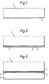
- a 2 1i m layer 3 of heavily doped p-type silicon is formed by diffusing boron into a 250 ⁇ m substrate 1 of intrinsic silicon.
- a Silox process a 0.1 1 1m coating 5 of silicon dioxide is deposited onto the diffused surfaces followed by a 0.2 ⁇ m coating 7 of silicon nitride deposited by chemical vapour deposition (Figure 2), to form passivation coatings.
- Figure 3 shows a 125 11m supporting layer 9 of polysilicon which is grown on top of the nitride coating 7 by chemical vapour deposition.
- the intrinsic silicon substrate 1 is the thinned ( Figure 4) to the required final thickness, which is of the order of 5 ⁇ rn, using a mixture of nitric acid, hydrogen fluoride and ethanoic acid. Phosphorus is then diffused into the exposed surface of the substrate to form an n-type layer 11 ( Figure 5).
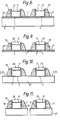
- a masking layer 13 is placed onto the substrate 1 ( Figure 6) and a mesa structure is formed by etching through the silicon as far as the nitride coating 7.
- the masking layer 13 is then removed and a passivation coating of silicon oxide 15 and silicon nitride 17 is deposited, followed by a further passivating coating of glass 19. Parts of the passivation coating (15, 17, 19) are removed to make a top contact 21 ( Figure 8). This contact 21 is then covered with a layer of metal 23.
- the substrate is mounted on a ceramic carrier (not shown) using wax and the polysilicon supporting layer 9 is etched away.
- Figure 10 shows the substrate with the exposed silicon nitride 7 and silicon dioxide 5 removed so as to open up the second diode contact 25.
- the silicon nitride is plasma etched with CF 4 :0 2 in the ratio 9:1.
- Buffered HF is used to etch the silicon dioxide layer.
- the second contact 25 is also metalised by evaporating a layer of titanium silver 27, onto the surface and covering the base of the wafer. The area is then plated with silver to a thickness of approximately 10-20)im.
- the top of the contact is then defined in photoresist and etched with a mixture of ammonium hydroxide, hydrogen peroxide and water.
- the individual diodes may then be separated ( Figure 11) by sawing through the metalised base layer 27.
Landscapes
- Chemical & Material Sciences (AREA)
- Organic Chemistry (AREA)
- Electrodes Of Semiconductors (AREA)
- Light Receiving Elements (AREA)
- Bipolar Transistors (AREA)
Description
- This invention relates to a method of manufacturing diodes and in particular to a method of manufacturing diodes comprising a region of intrinsic material between highly doped p-type and n-type layers to form a PIN diode.
- When there is no bias applied to a PIN diode, the intrinsic region is empty of tree charges. However, when the device is forward-biased, electrons from the n-type layer flow into the intrinsic region thus lowering the AC resistance of the device. In this way, as the DC current through the device increases, the AC resistance decreases.
- It is known to manufacture PIN diodes by diffusing p-type material into one surface and n-type material into the opposite surface of a thin slice of intrinsic silicon. Conventional PIN diodes have an intrinsic region of
thickness 5 to 10 11m. It is difficult to reduce the width of the intrinsic region of a diode made by presently-known techniques without impairing the quality of the intrinsic material; the transition regions become less abrupt and impurities diffuse into the intrinsic region. - It is an object of this invention to provide a method of manufacturing very thin PIN diodes whilst preserving the properties of the intrinsic material.
- According to the invention, a method of manufacturing a plurality of diodes comprises the steps of introducing a dopant of a first conductivity type into one surface of a layer of intrinsic material; growing a layer of supporting material onto the surface into which the dopant of said first conductivity type was introduced; introducing a dopant of a second conductivity type into the other surface of the layer of intrinsic material; and subsequently dividing the layer of intrinsic material into individual elements each of which constitutes a diode.
- Each resulting diode is therefore a PIN (or a NIP) diode in which the purity of the middle layer of intrinsic semiconductor material is preserved. As the intrinsic semiconductor material is supported by the supporting material, the intrinsic semiconductor material can be a very thin and fragile wafer or slice.
- Preferably a coating of a passivation material is formed on the surface of the intrinsic material where the layer of supporting material is to be grown.
- The coating of passivation material preferably comprises a layer of silicon dioxide overlaid with a layer of silicon nitride.
- The supporting material is preferably formed of polysilicon or of any grown material, provided that the material would not damage the intrinsic layer (e.g. by transfer of dopants). It acts to strengthen the substrate and facilitates the handling of the device during the manufacturing process. The material used should be capable of withstanding high temperatures and should have a temperature coefficient of expansion compatible with that of the semiconductor material. The intrinsic layer may then be thinned to a degree which is not practicable using other methods of manufacture, to produce a very thin device.
- After the intrinsic layer has been thinned, additionally removing any semiconductor material into which dopants of said first conductivity type have been introduced, to expose the surface of the intrinsic layer, dopants of a second conductivity type may be diffused into the exposed surface.
- The surface of the intrinsic layer into which the dopants of the second conductivity type are diffused may be masked. A mesa structure for the device can then be formed by etching through the intrinsic layer as far as the supporting layer.
- Conveniently, the masking layer is removed and further coatings of silicon oxide and silicon nitride are formed, for passivation. A further glass passivating layer may be formed over the oxide and nitride coatings.
- In order to make an electrical contact, the passivation coatings covering the semiconductor layer, into which dopants of said second conductivity type have been introduced, may be at least partially removed to expose the surface of the said semiconductor layer. A metal contact may then be formed on the exposed surface.
- After this, the supporting material is conveniently etched away, having mounted the wafer on a ceramic carrier using wax. The exposed areas of the passivation coating may then be removed also by etching so as to expose the semiconductor material doped with dopants of said first conductivity type. The exposed material is coated with metal to form the other diode contact.
- The other side of the semiconductor material doped with dopants of said first conductivity type is preferably plated with metal to form a base which acts as an integral heat sink. As the thermal paths to the heat sink are thus very short, this improves the power handling of the device.
- If the semiconductor materials used are highly doped, this improves the quality of the ohmic contacts.
- A method of manufacturing diodes in accordance with the invention will now be described, by way of example only, with reference to Figures 1 to 11.
- In Figure 1, a 21i
m layer 3 of heavily doped p-type silicon is formed by diffusing boron into a 250µm substrate 1 of intrinsic silicon. Using a Silox process a 0.1 11m coating 5 of silicon dioxide is deposited onto the diffused surfaces followed by a 0.2µm coating 7 of silicon nitride deposited by chemical vapour deposition (Figure 2), to form passivation coatings. - Figure 3 shows a 125
11m supporting layer 9 of polysilicon which is grown on top of thenitride coating 7 by chemical vapour deposition. - The
intrinsic silicon substrate 1 is the thinned (Figure 4) to the required final thickness, which is of the order of 5µrn, using a mixture of nitric acid, hydrogen fluoride and ethanoic acid. Phosphorus is then diffused into the exposed surface of the substrate to form an n-type layer 11 (Figure 5). - A
masking layer 13 is placed onto the substrate 1 (Figure 6) and a mesa structure is formed by etching through the silicon as far as thenitride coating 7. - As shown in Figure 7, the
masking layer 13 is then removed and a passivation coating ofsilicon oxide 15 andsilicon nitride 17 is deposited, followed by a further passivating coating ofglass 19. Parts of the passivation coating (15, 17, 19) are removed to make a top contact 21 (Figure 8). Thiscontact 21 is then covered with a layer ofmetal 23. In Figure 9, the substrate is mounted on a ceramic carrier (not shown) using wax and thepolysilicon supporting layer 9 is etched away. - Figure 10 shows the substrate with the exposed
silicon nitride 7 andsilicon dioxide 5 removed so as to open up the second diode contact 25. The silicon nitride is plasma etched with CF4:02 in the ratio 9:1. Buffered HF is used to etch the silicon dioxide layer. The second contact 25 is also metalised by evaporating a layer oftitanium silver 27, onto the surface and covering the base of the wafer. The area is then plated with silver to a thickness of approximately 10-20)im. The top of the contact is then defined in photoresist and etched with a mixture of ammonium hydroxide, hydrogen peroxide and water. - The individual diodes may then be separated (Figure 11) by sawing through the
metalised base layer 27.
Claims (8)
Applications Claiming Priority (2)
| Application Number | Priority Date | Filing Date | Title |
|---|---|---|---|
| GB8719309 | 1987-08-14 | ||
| GB878719309A GB8719309D0 (en) | 1987-08-14 | 1987-08-14 | Diodes |
Publications (2)
| Publication Number | Publication Date |
|---|---|
| EP0303390A1 EP0303390A1 (en) | 1989-02-15 |
| EP0303390B1 true EP0303390B1 (en) | 1990-10-31 |
Family
ID=10622327
Family Applications (1)
| Application Number | Title | Priority Date | Filing Date |
|---|---|---|---|
| EP88307157A Expired EP0303390B1 (en) | 1987-08-14 | 1988-08-03 | Manufacture of diodes |
Country Status (4)
| Country | Link |
|---|---|
| EP (1) | EP0303390B1 (en) |
| JP (1) | JP2816684B2 (en) |
| DE (1) | DE3860929D1 (en) |
| GB (2) | GB8719309D0 (en) |
Families Citing this family (6)
| Publication number | Priority date | Publication date | Assignee | Title |
|---|---|---|---|---|
| FR2676594B1 (en) * | 1991-05-17 | 1997-04-18 | Sgs Thomson Microelectronics | METHOD OF TAKING CONTACT ON A SEMICONDUCTOR COMPONENT. |
| DE4317721C1 (en) * | 1993-05-27 | 1994-07-21 | Siemens Ag | Process for separating chips from a wafer |
| US5656547A (en) * | 1994-05-11 | 1997-08-12 | Chipscale, Inc. | Method for making a leadless surface mounted device with wrap-around flange interface contacts |
| RU2393583C1 (en) * | 2009-06-19 | 2010-06-27 | Открытое акционерное общество "Оптрон" | Method of producing p-i-n diode crystals by group method (versions) |
| RU2452057C1 (en) * | 2011-02-17 | 2012-05-27 | Открытое акционерное общество "Оптрон" | Mode of fabrication of semiconductor shf limiter diodes by group method |
| RU2546856C2 (en) * | 2013-05-28 | 2015-04-10 | Закрытое акционерное общество "НИИМП-Т" | Production of semiconductor microwave devices |
Family Cites Families (2)
| Publication number | Priority date | Publication date | Assignee | Title |
|---|---|---|---|---|
| FR2520931B1 (en) * | 1982-02-02 | 1986-12-12 | Thomson Csf | COLLECTIVE PROCESS FOR MANUFACTURING MICROWAVE DIODES WITH BUILT-IN ENCAPSULATION AND DIODES OBTAINED THEREBY |
| FR2538616B1 (en) * | 1982-12-28 | 1986-01-24 | Thomson Csf | METHOD FOR THE COLLECTIVE MANUFACTURE OF MICROWAVE DIODES WITH INCORPORATED ENCAPSULATION AND DIODES THUS OBTAINED |
-
1987
- 1987-08-14 GB GB878719309A patent/GB8719309D0/en active Pending
-
1988
- 1988-08-03 GB GB8818486A patent/GB2208964B/en not_active Expired - Lifetime
- 1988-08-03 DE DE8888307157T patent/DE3860929D1/en not_active Expired - Lifetime
- 1988-08-03 EP EP88307157A patent/EP0303390B1/en not_active Expired
- 1988-08-10 JP JP63199768A patent/JP2816684B2/en not_active Expired - Lifetime
Also Published As
| Publication number | Publication date |
|---|---|
| GB2208964B (en) | 1991-02-06 |
| GB2208964A (en) | 1989-04-19 |
| GB8818486D0 (en) | 1988-09-07 |
| JP2816684B2 (en) | 1998-10-27 |
| GB8719309D0 (en) | 1987-09-23 |
| DE3860929D1 (en) | 1990-12-06 |
| EP0303390A1 (en) | 1989-02-15 |
| JPS6467977A (en) | 1989-03-14 |
Similar Documents
| Publication | Publication Date | Title |
|---|---|---|
| US4873205A (en) | Method for providing silicide bridge contact between silicon regions separated by a thin dielectric | |
| US3966577A (en) | Dielectrically isolated semiconductor devices | |
| CA1159966A (en) | Process of forming recessed dielectric regions in a monocrystalline silicon substrate | |
| EP0139165B1 (en) | Method of making a trench isolated integrated circuit device | |
| US4261095A (en) | Self aligned schottky guard ring | |
| EP0202240B1 (en) | Coating of iii-v and ii-vi compound semiconductors | |
| US4662956A (en) | Method for prevention of autodoping of epitaxial layers | |
| US3400309A (en) | Monolithic silicon device containing dielectrically isolatng film of silicon carbide | |
| US4343676A (en) | Etching a semiconductor material and automatically stopping same | |
| US4180422A (en) | Method of making semiconductor diodes | |
| US5677562A (en) | Planar P-N junction semiconductor structure with multilayer passivation | |
| CA1094429A (en) | Method of manufacturing a semiconductor device | |
| EP0076106B1 (en) | Method for producing a bipolar transistor | |
| US4900689A (en) | Method of fabrication of isolated islands for complementary bipolar devices | |
| US4373255A (en) | Method of making oxide passivated mesa epitaxial diodes with integral plated heat sink | |
| US3746587A (en) | Method of making semiconductor diodes | |
| US4032373A (en) | Method of manufacturing dielectrically isolated semiconductive device | |
| EP0111706B1 (en) | Sidewall isolation for gate of field effect transistor and process for the formation thereof | |
| EP0303390A1 (en) | Manufacture of diodes | |
| US4051507A (en) | Semiconductor structures | |
| US3447235A (en) | Isolated cathode array semiconductor | |
| US4210472A (en) | Manufacturing process of semiconductor devices | |
| US3519900A (en) | Temperature compensated reference diodes and methods for making same | |
| EP0206445A2 (en) | Process for forming a semiconductor cell in a silicon semiconductor body and a mixed CMOS/bipolar integrated circuit formed in a plurality of such cells | |
| KR880000483B1 (en) | Manufacturing method of semiconductor device |
Legal Events
| Date | Code | Title | Description |
|---|---|---|---|
| PUAI | Public reference made under article 153(3) epc to a published international application that has entered the european phase |
Free format text: ORIGINAL CODE: 0009012 |
|
| AK | Designated contracting states |
Kind code of ref document: A1 Designated state(s): DE FR |
|
| 17P | Request for examination filed |
Effective date: 19890203 |
|
| 17Q | First examination report despatched |
Effective date: 19900409 |
|
| GRAA | (expected) grant |
Free format text: ORIGINAL CODE: 0009210 |
|
| AK | Designated contracting states |
Kind code of ref document: B1 Designated state(s): DE FR |
|
| ET | Fr: translation filed | ||
| REF | Corresponds to: |
Ref document number: 3860929 Country of ref document: DE Date of ref document: 19901206 |
|
| PLBE | No opposition filed within time limit |
Free format text: ORIGINAL CODE: 0009261 |
|
| STAA | Information on the status of an ep patent application or granted ep patent |
Free format text: STATUS: NO OPPOSITION FILED WITHIN TIME LIMIT |
|
| 26N | No opposition filed | ||
| REG | Reference to a national code |
Ref country code: FR Ref legal event code: TP |
|
| REG | Reference to a national code |
Ref country code: FR Ref legal event code: TP |
|
| PGFP | Annual fee paid to national office [announced via postgrant information from national office to epo] |
Ref country code: DE Payment date: 20010730 Year of fee payment: 14 |
|
| PGFP | Annual fee paid to national office [announced via postgrant information from national office to epo] |
Ref country code: FR Payment date: 20010810 Year of fee payment: 14 |
|
| PG25 | Lapsed in a contracting state [announced via postgrant information from national office to epo] |
Ref country code: DE Free format text: LAPSE BECAUSE OF NON-PAYMENT OF DUE FEES Effective date: 20030301 |
|
| PG25 | Lapsed in a contracting state [announced via postgrant information from national office to epo] |
Ref country code: FR Free format text: LAPSE BECAUSE OF NON-PAYMENT OF DUE FEES Effective date: 20030430 |
|
| REG | Reference to a national code |
Ref country code: FR Ref legal event code: ST |
|
| REG | Reference to a national code |
Ref country code: FR Ref legal event code: CD Ref country code: FR Ref legal event code: CA |