EP0302730B1 - Isolated analog voltage sense circuit - Google Patents
Isolated analog voltage sense circuit Download PDFInfo
- Publication number
- EP0302730B1 EP0302730B1 EP88307220A EP88307220A EP0302730B1 EP 0302730 B1 EP0302730 B1 EP 0302730B1 EP 88307220 A EP88307220 A EP 88307220A EP 88307220 A EP88307220 A EP 88307220A EP 0302730 B1 EP0302730 B1 EP 0302730B1
- Authority
- EP
- European Patent Office
- Prior art keywords
- voltage
- capacitor
- input
- circuit
- output
- Prior art date
- Legal status (The legal status is an assumption and is not a legal conclusion. Google has not performed a legal analysis and makes no representation as to the accuracy of the status listed.)
- Expired - Lifetime
Links
Images


Classifications
-
- H—ELECTRICITY
- H02—GENERATION; CONVERSION OR DISTRIBUTION OF ELECTRIC POWER
- H02M—APPARATUS FOR CONVERSION BETWEEN AC AND AC, BETWEEN AC AND DC, OR BETWEEN DC AND DC, AND FOR USE WITH MAINS OR SIMILAR POWER SUPPLY SYSTEMS; CONVERSION OF DC OR AC INPUT POWER INTO SURGE OUTPUT POWER; CONTROL OR REGULATION THEREOF
- H02M3/00—Conversion of dc power input into dc power output
- H02M3/22—Conversion of dc power input into dc power output with intermediate conversion into ac
- H02M3/24—Conversion of dc power input into dc power output with intermediate conversion into ac by static converters
- H02M3/28—Conversion of dc power input into dc power output with intermediate conversion into ac by static converters using discharge tubes with control electrode or semiconductor devices with control electrode to produce the intermediate ac
- H02M3/325—Conversion of dc power input into dc power output with intermediate conversion into ac by static converters using discharge tubes with control electrode or semiconductor devices with control electrode to produce the intermediate ac using devices of a triode or a transistor type requiring continuous application of a control signal
- H02M3/335—Conversion of dc power input into dc power output with intermediate conversion into ac by static converters using discharge tubes with control electrode or semiconductor devices with control electrode to produce the intermediate ac using devices of a triode or a transistor type requiring continuous application of a control signal using semiconductor devices only
Definitions
- This invention relates to the field of isolated sensor circuits and more particularly to an isolated voltage sensing circuit which is adapted for use with switching power supplies.
- Switching power supplies are well known for their excellent performance over a wide range of load conditions and operating temperatures. Examples of switching power supplies include forward converter and flyback designs. Switching power supplies are typically used to convert a first DC voltage, e.g., a high input voltage, into a second DC voltage, e.g. a voltage which is relatively low. Since these power supplies typically use transformers for energy conversion, they are used in applications which require input/output isolation.
- An example of a switching power supply having input/output isolating is disclosed in U.S. Patent No. 4,323,961 issued to Elliot Josephson.
- an isolated power supply requires some means for sensing its output voltage to complete the regulator loop. To preserve input/output isolation, it is essential that the sensed output voltage is also fed back via an isolator circuit.
- Typical isolators include opto-isolators or feedback isolation transformers. In situations where a high degree of isolation is required, most prior art sensors have been quite complex and expensive.
- a DC amplifier supplies power to a first series coupled diode and condenser through an electronic switch which is driven by a pulse generator.
- This diode and condensor combination is coupled across the primary winding of a transformer.
- An identical second diode and condenser combination is coupled across the secondary winding of the transformer.
- Feedback is provided to the DC amplifier through a resistor which is coupled between the inverting input of the DC amplifier and the common terminal of said first diode and condensor combination.
- the active circuitry is located on the primary side of the transformer and is therefore subject to damage from any high voltage which may appear thereon.
- the device Since a DC amplifier is used to drive the primary of the transformer, the device is also subject to variations in linearity over a range of temperatures. Furthermore, this circuit is more complex than is desirable because it requires identical diode and condenser combinations on both sides of the transformer to generate an isolated voltage. Any variation in the matching between these identical circuits will affect the accuracy of the device. While this device discloses a single transformer structure, it is disadvantageous because it does not provide a controlled discharge path for the capacitor and it cannot respond to signals with fast fall times. Furthermore, the capacitor voltage cannot be held constant due to leakage through a resistor.
- isolated sensors are also used in a variety of other applications.
- isolated sensors are often used in data acquisition applications to protect computer data input lines from spurious DC signals appearing thereon.
- Isolated sensors are also widely used in medical applications where it is critical to protect a patient from any high voltage which may be generated by medical testing equipment.
- instrumentation grade isolation amplifier One type of isolated sensor that is often used in medical instrumentation devices is the instrumentation grade isolation amplifier.
- instrumentation grade isolation amplifiers are necessarily quite complex and as such they are among the most expensive of all isolation devices. The expense of devices of this type prohibits their use in power supply applications.
- an isolated sensor circuit comprising sensor means sensing the input voltage, transformer means having input and output windings, desirable isolated from one another, for coupling the input voltage sensed by the sensor means to the output winding, capacitor means connected to the output winding through switching means so that they are coupled by the transformer means to the input voltage sensed by the sensor means, and a clock signal output providing a repeating oscillating signal, the switching means being responsive to the clock signal output for repeatedly connecting and disconnecting the output winding to the capacitor means, whereby the capacitor means will charge or discharge during the period that the switching means are conductive so that the voltage of the charge progressively moves at each cycle of the clock means towards a figure matching the voltage sensed by the sensing means, the output voltage of the capacitor means therefore providing a voltage which follows the input voltage.
- the circuit according to the invention provides an isolated sensor which does not require synchronization between the circuitry on either side of the transformer.
- the sensor also has improved bandwidth and stability over temperature and time.
- the active circuitry is located entirely on the sensor output side of the transformer opposite the voltage to be sensed.
- the active circuitry generally comprises a switching device coupled in series between the output of the sensor and one side of the output winding of the transformer.
- the switching device and a current source periodically function to control the amount of charge on a capacitor coupled across the output of the device as a function of the sensed input voltage.
- the charge developed across the capacitor will be at substantially the same voltage as the voltage coupled to the input winding of the transformer, the transformer functioning to provide isolation between the input voltage and the sensor output.
- the capacitor substantially retains this voltage during the time that the switching device is off.
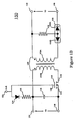
- an exemplary embodiment 100 of an isolated analog voltage sense circuit is shown for sensing a voltage V1 appearing at input terminals 104 and 105.
- a 1:1 transformer 102 including first and second windings 102A and 102B, is used to couple the input to the output of the device.
- One terminal of winding 102A of transformer 102 is coupled to input terminal 104 through twin diodes 106.
- Twin diodes 106 include diodes 106A and 106B whose cathodes are connected in common.
- the anode of twin diode 106A is coupled to the input terminal 104 and the anode of twin diode 106B is coupled to one terminal of winding 102A.
- the other terminal of winding 102A is coupled directly to terminal 105.
- a resistor 108 is coupled between the common cathode of the twin diodes 106 and terminal 105.
- the primary active element is switching device 110 which preferably comprises a FET transistor.
- the drain terminal 112 of switching device 110 is coupled to one terminal of winding 102B.
- the source terminal 114 of switching device 110 is coupled to one side of a capacitor 116 and to an output terminal 118.
- the gate terminal 120 of switching device 110 is coupled to a clock signal input terminal 122.
- An appropriate clock signal derived from a conventional clock generator (not shown), is coupled to input terminal 122.
- a diode 124 and resistor 126 are connected in series between terminal 122 and the side of capacitor 116 opposite to the side connected to terminal 118. This side of capacitor 116 is also coupled to output terminal 128 and to the other terminal of winding 102B.
- a voltage is developed across resistor 108 which is equal to the sensed voltage V1 less a voltage drop V D across diode 106A.
- switching device 110 is turned 'on' and capacitor 116 is provided with a charging current by diode 124 and resistor 126.
- Capacitor 116 continues to charge until the voltage V2 across capacitor 116 reaches the sum of the voltage across resistor 108 and twin diode 106B. At this point, further charging current from resistor 126 is diverted to ground through the 1:1 transformer 102. If the value of voltage V1 later changes such that the voltage across capacitor 116 now exceeds V1, during the next positive cycle of CLK capacitor 116 will discharge through the same path a sufficient amount such that V2 equals the new value of V1.
- switching device 110 On the negative cycle of CLK, switching device 110 is turned 'off' and diode 124 blocks the flow of any current in a reverse direction through resistor 126. At this point, the charge present on capacitor 116 will be substantially equal to V1. This charge will remain on capacitor 116 until the next positive occurrence of CLK independent of any change in V1 during this CLK low cycle. While switching device 110 is off, capacitor 116 is isolated from transformer 102, enabling transformer 102 to reset.
- twin diodes 106 are used to cancel any voltage offset error which would be introduced by a single diode.
- the specific diodes used to implement the twin diodes 106 are not critical to this invention but a BAS 16 may be advantageously employed.
- Diode 124 may be a BAV 70. Both of these diodes are available from U.S. Philips.
- Resistor 108 may be approximately 100 ohms, and resistor 126 may be approximately 330 ohms.
- Capacitor 116 may be approximately 0.01 microfarads.
- the switching device 110 may be an n-channel MOSFET, such as a 2N7002, although a variety of other switching devices could be substituted therefor.
- the clock signal coupled to terminal 122 may be generated by a wide variety of circuits, and the actual switching speed will vary from application to application. However, the frequency and duty cycle of the clock signal may limit the bandwidth and slew rate of isolated sensor 100.
- a suitable clock signal is a square wave signal having a 5.6 V peak voltage with a 15% duty cycle and a 500 KHz operating frequency. Voltages in the range of 2.5 V ⁇ 0.5 V may be detected with the circuit 100 using this clock signal.
- FIG. 1B is a schematic diagram depicting a second embodiment 150 of the present invention.
- the circuit 150 is a modification of the circuit 100 of Figure 1A wherein the twin diode 106 is replaced by twin diode 156.
- Twin diode 106 is configured such that diodes 106A and 106B are coupled with a common cathode connection. This allows twin diode 106 to be placed on the positive input side of the circuit.
- the teachings of the present invention provide that a common anode diode 156 may be substituted for twin diode 106 if it is placed on the negative input side of the circuit as shown in Figure 1B. Therefore, the anode of diode 156A is coupled directly to terminal 105.
- the anode of diode 156B is coupled to one terminal of winding 102A and the other terminal of winding 102A is coupled directed to terminal 104.
- a resistor 108 is disposed between terminal 104 and the common cathode connection of twin diode 156.
- FIG. 2A there is shown a preferred embodiment 200 of an isolated analog voltage sense circuit according to the present invention.
- the circuit 200 employs the same basic configuration as the circuit 100 but incorporates additional components which improve the operation and stability of the circuit.
- similar elements bear the same numbers as the elements in Figure 1A. Only the new elements are discussed in detail herein.
- the preferred embodiment 200 includes input terminals 104 and 105, which are coupled to the voltage V1 to be sensed.
- Terminal 104 is coupled to the non-inverting input of an amplifier 206 which presents a high impedance at terminal 104.
- the output of amplifier 206 is coupled to a resistor network comprising resistors 208 and 210. Resistor 208 cooperates with capacitor 214 to stabilize amplifier 206. Resistor 210 pre-loads the output stage of amplifier 206 to improve its current sinking capability.
- One end of resistor 210 is coupled to a negative power supply -V at terminal 212.
- the common junction of resistors 208 and 210 is coupled to one side of capacitor 214 and to the common cathode connection of twin diode 106.
- the anode of twin diode 106A is coupled to a pullup resistor 218 and the inverting input of amplifier 206.
- the opposite end of resistor 218 is coupled to a voltage source +V at terminal 220 to provide a biasing current for diode 106A. Without this biasing current, a 0.6V drop across diode 106A cannot be maintained with this circuit configuration.
- the anode of twin diode 106B is coupled to one side of winding 102A of transformer 102.
- the other side of winding 102A is coupled to terminal 105 and the other side of capacitor 214.
- Amplifier 206 stabilizes the voltage across capacitor 214 to a voltage which is equal to the input voltage V1 minus the diode drop caused by diode 106A in its feedback loop. Therefore, the maximum voltage developed across winding 102A and hence 102B of transformer 102 will be equivalent to the input voltage V1.
- the preferred embodiment 200 also employs a 1:1 transformer 102 to couple the input voltage V1 to the output of the sensor device.
- a FET switching device 110 is coupled in series between one side of winding 102B of transformer 102 and terminal 118 which is one output terminal of the device.
- the other output terminal 128 of isolated sensor 200 is coupled the other side of winding 102B of transformer 102.
- the FET 110 is switched 'on' by a clock signal (CLK) appearing at terminal 122 which is coupled to the gate of FET 110.
- CLK clock signal
- the clock signal described herein may have the same characteristics as the clock signal described in conjunction with Figure 1A.
- a capacitor 116 is connected between terminals 118 and 128.
- the circuit 200 provides another improvement over the circuit 100 by including a capacitor 246 which is coupled between the cathode of diode 124 and the terminal 118.
- capacitor 246 prevents capacitor 116 from discharging by applying a charging voltage to capacitor 116 for a brief period during the negative transition of CLK. More specifically, the voltage VC246 will rise to the peak voltage of CLK less one diode drop caused by diode 124 once CLK is high, and will discharge to V C116 via R126 for a brief period during the falling edge of CLK. This compensates for the parasitic effects caused by switching speed of FET 110 and interwinding capacitance of transformer 102.
- the voltage V C116 and thus V2 may further drop slightly because of the discharging of capacitor 116 as a function of the impedence of the circuit coupled to the output of the sensor device. In such a case the voltage drop across capacitor 116 will be off only a fraction of a percent from its nominal operating voltage. Typically, the voltage drop V C116 due to loading may be in the range of 0.2 mV over the 2.5 V input voltage.
- FIG 2B is a schematic diagram depicting a fourth embodiment 250 of the present invention.
- the circuit of 250 is a modification of the circuit 200 of Figure 2A wherein a common anode twin diode 256 is substituted for the common cathode twin diode 106. Since this embodiment employs a twin diode which is coupled to the negative side of the circuit, a resistor 258 is coupled between the negative power supply input terminal -V e and the common connection of the cathode of diode 256A and the inverting input of amplifier 206.
- capacitor 214 is replaced by capacitor 258 which is coupled between the positive input terminal and the common anode terminal of twin diode 265.
- a resistor 260 is coupled between the output terminal of amplifier 206 and the common connection of twin diode 256 and capacitor 258. This common connection is further coupled to resistor 262. The other terminal of resistor 262 is coupled to the positive power supply input terminal +V e .
- FIG. 3 is a series of graphs which depict the various operating waveforms of the present invention.
- V C116 the voltage present on capacitor 116
- the improved isolated sensor circuit employs a single switching device to charge a capacitor on the sensor output side of a transformer.
- the switching device may be controlled by an external clock signal and does not require any type of synchronization.
- the present invention achieves improved performance without requiring a complex transformer structure or multiple switching devices.
Abstract
Description
- This invention relates to the field of isolated sensor circuits and more particularly to an isolated voltage sensing circuit which is adapted for use with switching power supplies.
- Switching power supplies are well known for their excellent performance over a wide range of load conditions and operating temperatures. Examples of switching power supplies include forward converter and flyback designs. Switching power supplies are typically used to convert a first DC voltage, e.g., a high input voltage, into a second DC voltage, e.g. a voltage which is relatively low. Since these power supplies typically use transformers for energy conversion, they are used in applications which require input/output isolation. An example of a switching power supply having input/output isolating is disclosed in U.S. Patent No. 4,323,961 issued to Elliot Josephson.
- As with any type of regulated power supply, an isolated power supply requires some means for sensing its output voltage to complete the regulator loop. To preserve input/output isolation, it is essential that the sensed output voltage is also fed back via an isolator circuit. Typical isolators include opto-isolators or feedback isolation transformers. In situations where a high degree of isolation is required, most prior art sensors have been quite complex and expensive.
- One type of isolated sensor is described in U.S. Patent No. 4,030,041, by Sasaki. In this device, a signal derived from the primary winding of a transformer is used to switch an optical isolator. The output of the optical isolator is used to control a FET switching device which is coupled between one secondary winding of the transformer and a buffer amplifier. A capacitor is also coupled to the input of the buffer amplifier. The Sasaki invention relies on a transformer having a primary and four secondary windings and an optical isolator to unite the operation of the device. This device has several disadvantages. For example, since the isolation transformer is embedded into the line power transformer, the bandwidth of the device is limited. Since the operation of the device is synchronized to a supplied line frequency, its operation is also relatively slow. Furthermore, switching devices which rely on optical isolators to provide isolation between primary and secondary control signals typically exhibit poor stability over time and temperature.
- A somewhat simpler device is disclosed in U.S. Patent No. 3,931,582, issued to Kato, et al. In this device, a DC amplifier supplies power to a first series coupled diode and condenser through an electronic switch which is driven by a pulse generator. This diode and condensor combination is coupled across the primary winding of a transformer. An identical second diode and condenser combination is coupled across the secondary winding of the transformer. Feedback is provided to the DC amplifier through a resistor which is coupled between the inverting input of the DC amplifier and the common terminal of said first diode and condensor combination. In this device, the active circuitry is located on the primary side of the transformer and is therefore subject to damage from any high voltage which may appear thereon. Since a DC amplifier is used to drive the primary of the transformer, the device is also subject to variations in linearity over a range of temperatures. Furthermore, this circuit is more complex than is desirable because it requires identical diode and condenser combinations on both sides of the transformer to generate an isolated voltage. Any variation in the matching between these identical circuits will affect the accuracy of the device. While this device discloses a single transformer structure, it is disadvantageous because it does not provide a controlled discharge path for the capacitor and it cannot respond to signals with fast fall times. Furthermore, the capacitor voltage cannot be held constant due to leakage through a resistor.
- Other types of sensors employ devices known as choppers or synchro-rectifiers which synchronize the operation of the sensor circuitry. In this class of device, two transformers are required; one for the sensed analog signal and one for the synchronization signal. Still other chopper or synchro-rectifiers employ a single transformer having multiple secondary windings therein to operate the switching device. An example of an isolated sensor of this type is shown in U.S. Patent No. 4,506,230 by Ashley-Rollman and in U.S. Patent No. 4,286,225 by Morong. In each of these references, a complicated transformer structure is required. As a result, the capacitive coupling between each side of the circuit is relatively high. Furthermore, each of these references requires active components on the input side of the circuit thus requiring a relatively stable isolated power supply.
- While the above discussion discloses the use of isolated sensors in switching power supplies, isolated sensors are also used in a variety of other applications. For example, isolated sensors are often used in data acquisition applications to protect computer data input lines from spurious DC signals appearing thereon. Isolated sensors are also widely used in medical applications where it is critical to protect a patient from any high voltage which may be generated by medical testing equipment.
- One type of isolated sensor that is often used in medical instrumentation devices is the instrumentation grade isolation amplifier. One example of an instrumentation grade isolation amplifier is shown in U.S. Patent No. 3,946,324 by Smith. Instrumentation grade isolation amplifiers are necessarily quite complex and as such they are among the most expensive of all isolation devices. The expense of devices of this type prohibits their use in power supply applications.
- From the foregoing, it can be seen that no device is known which provides a high degree of isolation at low cost, without requiring an optical isolator, a synchronizing signal or a complicated transformer structure to construct the isolated sensor.
- Accordingly, it is an object of the present invention to provide an improved isolated sensor having a minimum number of components.
- According to the invention there is provided an isolated sensor circuit comprising sensor means sensing the input voltage, transformer means having input and output windings, desirable isolated from one another, for coupling the input voltage sensed by the sensor means to the output winding, capacitor means connected to the output winding through switching means so that they are coupled by the transformer means to the input voltage sensed by the sensor means, and a clock signal output providing a repeating oscillating signal, the switching means being responsive to the clock signal output for repeatedly connecting and disconnecting the output winding to the capacitor means, whereby the capacitor means will charge or discharge during the period that the switching means are conductive so that the voltage of the charge progressively moves at each cycle of the clock means towards a figure matching the voltage sensed by the sensing means, the output voltage of the capacitor means therefore providing a voltage which follows the input voltage.
- The circuit according to the invention provides an isolated sensor which does not require synchronization between the circuitry on either side of the transformer. The sensor also has improved bandwidth and stability over temperature and time. Further the active circuitry is located entirely on the sensor output side of the transformer opposite the voltage to be sensed. The active circuitry generally comprises a switching device coupled in series between the output of the sensor and one side of the output winding of the transformer. The switching device and a current source periodically function to control the amount of charge on a capacitor coupled across the output of the device as a function of the sensed input voltage. The charge developed across the capacitor will be at substantially the same voltage as the voltage coupled to the input winding of the transformer, the transformer functioning to provide isolation between the input voltage and the sensor output. The capacitor substantially retains this voltage during the time that the switching device is off.
- The invention will now be described, by way of example, with reference to the accompanying drawings, in which:
- Figure 1A is a schematic diagram of a first embodiment of the invention;
- Figure 1B is a schematic diagram of a second embodiment of the present invention;
- Figure 2A is a schematic diagram of the presently preferred embodiment of the invention;
- Figure 2B is a schematic diagram of a fourth embodiment of the invention; and
- Figure 3 illustrates various operating waveforms of the circuit shown in Figure 2A.
- Referring to Figure 1A, an
exemplary embodiment 100 of an isolated analog voltage sense circuit is shown for sensing a voltage V1 appearing atinput terminals transformer 102, including first andsecond windings transformer 102 is coupled toinput terminal 104 throughtwin diodes 106.Twin diodes 106 includediodes twin diode 106A is coupled to theinput terminal 104 and the anode oftwin diode 106B is coupled to one terminal of winding 102A. The other terminal of winding 102A is coupled directly toterminal 105. Aresistor 108 is coupled between the common cathode of thetwin diodes 106 andterminal 105. - All of the active circuitry of the
isolated sensor 100 is located on the sensor output side of thetransformer 102. The primary active element is switchingdevice 110 which preferably comprises a FET transistor. Thedrain terminal 112 of switchingdevice 110 is coupled to one terminal of winding 102B. Thesource terminal 114 of switchingdevice 110 is coupled to one side of acapacitor 116 and to anoutput terminal 118. Thegate terminal 120 of switchingdevice 110 is coupled to a clocksignal input terminal 122. An appropriate clock signal, derived from a conventional clock generator (not shown), is coupled to input terminal 122. - A
diode 124 andresistor 126 are connected in series betweenterminal 122 and the side ofcapacitor 116 opposite to the side connected toterminal 118. This side ofcapacitor 116 is also coupled tooutput terminal 128 and to the other terminal of winding 102B. - In operation, a voltage is developed across
resistor 108 which is equal to the sensed voltage V1 less a voltage drop VD acrossdiode 106A. On the positive cycle of the clock signal (CLK) appearing atterminal 122, switchingdevice 110 is turned 'on' andcapacitor 116 is provided with a charging current bydiode 124 andresistor 126.Capacitor 116 continues to charge until the voltage V2 acrosscapacitor 116 reaches the sum of the voltage acrossresistor 108 andtwin diode 106B. At this point, further charging current fromresistor 126 is diverted to ground through the 1:1transformer 102. If the value of voltage V1 later changes such that the voltage acrosscapacitor 116 now exceeds V1, during the next positive cycle ofCLK capacitor 116 will discharge through the same path a sufficient amount such that V2 equals the new value of V1. - On the negative cycle of CLK, switching
device 110 is turned 'off' anddiode 124 blocks the flow of any current in a reverse direction throughresistor 126. At this point, the charge present oncapacitor 116 will be substantially equal to V1. This charge will remain oncapacitor 116 until the next positive occurrence of CLK independent of any change in V1 during this CLK low cycle. While switchingdevice 110 is off,capacitor 116 is isolated fromtransformer 102, enablingtransformer 102 to reset. - According to the teachings of the present invention,
twin diodes 106 are used to cancel any voltage offset error which would be introduced by a single diode. The specific diodes used to implement thetwin diodes 106 are not critical to this invention but a BAS 16 may be advantageously employed.Diode 124 may be a BAV 70. Both of these diodes are available from U.S. Philips.Resistor 108 may be approximately 100 ohms, andresistor 126 may be approximately 330 ohms.Capacitor 116 may be approximately 0.01 microfarads. Theswitching device 110 may be an n-channel MOSFET, such as a 2N7002, although a variety of other switching devices could be substituted therefor. - The clock signal coupled to
terminal 122 may be generated by a wide variety of circuits, and the actual switching speed will vary from application to application. However, the frequency and duty cycle of the clock signal may limit the bandwidth and slew rate ofisolated sensor 100. One example of a suitable clock signal is a square wave signal having a 5.6 V peak voltage with a 15% duty cycle and a 500 KHz operating frequency. Voltages in the range of 2.5 V± 0.5 V may be detected with thecircuit 100 using this clock signal. - Figure 1B is a schematic diagram depicting a
second embodiment 150 of the present invention. Thecircuit 150 is a modification of thecircuit 100 of Figure 1A wherein thetwin diode 106 is replaced bytwin diode 156.Twin diode 106 is configured such thatdiodes twin diode 106 to be placed on the positive input side of the circuit. The teachings of the present invention provide that acommon anode diode 156 may be substituted fortwin diode 106 if it is placed on the negative input side of the circuit as shown in Figure 1B. Therefore, the anode ofdiode 156A is coupled directly toterminal 105. The anode ofdiode 156B is coupled to one terminal of winding 102A and the other terminal of winding 102A is coupled directed toterminal 104. Aresistor 108 is disposed betweenterminal 104 and the common cathode connection oftwin diode 156. - Referring now to Figure 2A, there is shown a
preferred embodiment 200 of an isolated analog voltage sense circuit according to the present invention. Thecircuit 200 employs the same basic configuration as thecircuit 100 but incorporates additional components which improve the operation and stability of the circuit. In the description of this embodiment of the present invention, similar elements bear the same numbers as the elements in Figure 1A. Only the new elements are discussed in detail herein. - The
preferred embodiment 200 includesinput terminals Terminal 104 is coupled to the non-inverting input of anamplifier 206 which presents a high impedance atterminal 104. The output ofamplifier 206 is coupled to a resistornetwork comprising resistors Resistor 208 cooperates withcapacitor 214 to stabilizeamplifier 206.Resistor 210 pre-loads the output stage ofamplifier 206 to improve its current sinking capability. One end ofresistor 210 is coupled to a negative power supply -V atterminal 212. The common junction ofresistors capacitor 214 and to the common cathode connection oftwin diode 106. The anode oftwin diode 106A is coupled to apullup resistor 218 and the inverting input ofamplifier 206. The opposite end ofresistor 218 is coupled to a voltage source +V at terminal 220 to provide a biasing current fordiode 106A. Without this biasing current, a 0.6V drop acrossdiode 106A cannot be maintained with this circuit configuration. The anode oftwin diode 106B is coupled to one side of winding 102A oftransformer 102. The other side of winding 102A is coupled toterminal 105 and the other side ofcapacitor 214. -
Amplifier 206 stabilizes the voltage acrosscapacitor 214 to a voltage which is equal to the input voltage V1 minus the diode drop caused bydiode 106A in its feedback loop. Therefore, the maximum voltage developed across winding 102A and hence 102B oftransformer 102 will be equivalent to the input voltage V1. - The
preferred embodiment 200 also employs a 1:1transformer 102 to couple the input voltage V1 to the output of the sensor device. AFET switching device 110 is coupled in series between one side of winding 102B oftransformer 102 and terminal 118 which is one output terminal of the device. Theother output terminal 128 ofisolated sensor 200 is coupled the other side of winding 102B oftransformer 102. TheFET 110 is switched 'on' by a clock signal (CLK) appearing atterminal 122 which is coupled to the gate ofFET 110. The clock signal described herein may have the same characteristics as the clock signal described in conjunction with Figure 1A. Acapacitor 116 is connected betweenterminals FET 110 turns 'on' andcapacitor 116 is charged by CLK through a series connecteddiode 124 andresistor 126. Accordingly, a voltage is developed acrosscapacitor 116 and thus acrossoutput terminals - The
circuit 200 provides another improvement over thecircuit 100 by including acapacitor 246 which is coupled between the cathode ofdiode 124 and the terminal 118. During the falling edge of CLK, the inherent capacitance ofFET 110 together with the parasitic capacitance across winding102B cause capacitor 116 to discharge slightly. The addition ofcapacitor 246 preventscapacitor 116 from discharging by applying a charging voltage tocapacitor 116 for a brief period during the negative transition of CLK. More specifically, the voltage VC246 will rise to the peak voltage of CLK less one diode drop caused bydiode 124 once CLK is high, and will discharge to VC116 via R126 for a brief period during the falling edge of CLK. This compensates for the parasitic effects caused by switching speed ofFET 110 and interwinding capacitance oftransformer 102. - The voltage VC116 and thus V2 may further drop slightly because of the discharging of
capacitor 116 as a function of the impedence of the circuit coupled to the output of the sensor device. In such a case the voltage drop acrosscapacitor 116 will be off only a fraction of a percent from its nominal operating voltage. Typically, the voltage drop VC116 due to loading may be in the range of 0.2 mV over the 2.5 V input voltage. - Figure 2B is a schematic diagram depicting a
fourth embodiment 250 of the present invention. The circuit of 250 is a modification of thecircuit 200 of Figure 2A wherein a commonanode twin diode 256 is substituted for the commoncathode twin diode 106. Since this embodiment employs a twin diode which is coupled to the negative side of the circuit, aresistor 258 is coupled between the negative power supply input terminal -Ve and the common connection of the cathode ofdiode 256A and the inverting input ofamplifier 206. In thecircuit 250,capacitor 214 is replaced bycapacitor 258 which is coupled between the positive input terminal and the common anode terminal of twin diode 265. Aresistor 260 is coupled between the output terminal ofamplifier 206 and the common connection oftwin diode 256 andcapacitor 258. This common connection is further coupled toresistor 262. The other terminal ofresistor 262 is coupled to the positive power supply input terminal +Ve. Those skilled in the art will appreciate that the operation of thecircuits twin diodes - Figure 3 is a series of graphs which depict the various operating waveforms of the present invention. Prior to the point where the input voltage V1 is present, the voltage present on capacitor 116 (VC116) will be approximately zero volts. When a voltage V1 is applied to the input terminals, the voltage VT102 across the windings of
transformer 102 will rise to a voltage equal to V1. Responsive to this voltage,capacitor 116 will begin to charge upon the positive occurrence of CLK. If V1 is then reduced to a lower value, the voltage VT102 will be clamped to a voltage no higher than V1.Capacitor 116 will be discharged to V1 upon the occurrence of a positive cycle of the CLK. - In summary, the improved isolated sensor circuit employs a single switching device to charge a capacitor on the sensor output side of a transformer. The switching device may be controlled by an external clock signal and does not require any type of synchronization. The present invention achieves improved performance without requiring a complex transformer structure or multiple switching devices.
Claims (10)
- An isolated sensor circuit comprising transformer means (102) having isolated input (102A) and output (102B) windings for coupling an input voltage to the output winding (102B), characterised in that sensor means (106,256) sense the input voltage for application to the input winding (102A), capacitor means (116) are connected to the output winding (102B) through switching means (110) so that they are coupled by the transformer means (102) to the input voltage sensed by the sensor means (106, 256) and a clock signal output (122) provides a repeating oscillating signal, the switching means (110) being responsive to the clock signal output to repeatedly connect and disconnect the output winding (102B) to the capacitor means (116), whereby the capacitor means (116) will charge or discharge during the period that the switching means (110) are conductive so that the voltage of the charge progressively moves at each cycle of the clock means towards a figure matching the input voltage sensed by the sensing means, the output voltage of the capacitor means (116) therefore providing a voltage which follows the input voltage.
- A circuit as claimed in Claim 1 characterised in that the sensor means (106, 256) comprise twin diodes (106A, 106B, 256A, 256B) having a common node, the twin diodes being disposed in an opposed relation relative one another with respect to the common node, one terminal of the twin diodes (106A, 106B, 256A, 256B) being connected to the input winding (102A) and the opposite terminal of the twin diodes (106A, 106B, 256A, 256B) being connected to the input voltage.
- A circuit as claimed in Claim 2 characterised in that the twin diodes (106A, 106B, 256A, 256B) are coupled in a common cathode configuration.
- A circuit as claimed in Claim 2 characterised that the twin diodes (106A, 106B, 256A, 256B) are coupled in a common anode configuration.
- A circuit as claimed in any of claims 2 to 4 characterised in that sensor means (106, 256) further comprise a resistor (210) coupled between the common node of the twin diodes (106A, 106B, 256A, 256B) and the input winding (102A) of the transformer means (102), the input voltage being applied across the said opposite terminal of the twin diodes (106A, 106B, 256A, 256B) and the resistor (210).
- A circuit as claimed in any of claims 2 to 4 characterised in that the sensor means (106, 256) further comprise amplifier means (206) having inverting and non-inverting input terminals and an output terminal, a capacitor (214, 258) coupled between the common node and the input winding (102A), and a first resistor (208, 260) in series between the common node and the output terminal of the amplifier (206), the input voltage to be sensed being applied to one of the input terminals of the amplifier.
- A circuit as claimed in Claim 6 characterised in that it further comprises a first voltage source applied via a second resistor (218, 258) to bias one of the diodes (106A, 256A), and a second voltage source connected to the common node via a third resistor (210, 262) to pre-load the output terminal of the amplifier to improve its current sinking capability.
- A circuit as claimed in any preceding claim chararterised in that the transformer means (102) is a 1:1 transformer.
- A circuit as claimed in any preceding claim characterised in that the switching means (110) further comprise rectifier means (124) in series with resistor means (126), the output voltage from the output winding (102B) generating a current through the resistor means (126) when the switch means are closed to provide a voltage drop for charging the capacitor means (116).
- A circuit as claimed in any preceding claim characterised in that it comprises additional capacitor means (246) in parallel with the capacitor means (116) to apply a charging voltage to the said capacitor means (116) during the switching off of the switching means (110), to prevent unintentional discharge of the capacitor means (116) during switching off of the switching means (110).
Priority Applications (1)
| Application Number | Priority Date | Filing Date | Title |
|---|---|---|---|
| AT88307220T ATE82447T1 (en) | 1987-08-05 | 1988-08-04 | ISOLATED ANALOG VOLTAGE SENSING CIRCUIT. |
Applications Claiming Priority (2)
| Application Number | Priority Date | Filing Date | Title |
|---|---|---|---|
| US81840 | 1987-08-05 | ||
| US07/081,840 US4949030A (en) | 1987-08-05 | 1987-08-05 | Isolated analog voltage sense circuit |
Publications (3)
| Publication Number | Publication Date |
|---|---|
| EP0302730A2 EP0302730A2 (en) | 1989-02-08 |
| EP0302730A3 EP0302730A3 (en) | 1989-11-23 |
| EP0302730B1 true EP0302730B1 (en) | 1992-11-11 |
Family
ID=22166732
Family Applications (1)
| Application Number | Title | Priority Date | Filing Date |
|---|---|---|---|
| EP88307220A Expired - Lifetime EP0302730B1 (en) | 1987-08-05 | 1988-08-04 | Isolated analog voltage sense circuit |
Country Status (6)
| Country | Link |
|---|---|
| US (1) | US4949030A (en) |
| EP (1) | EP0302730B1 (en) |
| JP (1) | JPH0196566A (en) |
| CN (1) | CN1012873B (en) |
| AT (1) | ATE82447T1 (en) |
| DE (1) | DE3875849D1 (en) |
Families Citing this family (14)
| Publication number | Priority date | Publication date | Assignee | Title |
|---|---|---|---|---|
| EP0447405B1 (en) * | 1988-12-06 | 1995-08-02 | Boral Johns Perry Industries Pty. Ltd. | Control system for a motor |
| US5808495A (en) * | 1991-11-26 | 1998-09-15 | Furuno Electric Company, Limited | Magnetron driving circuit |
| US5742153A (en) * | 1992-08-18 | 1998-04-21 | Basic Measuring Instruments | Coasting power supply for AC power system waveform measuring instrument |
| US6351530B1 (en) | 1998-11-16 | 2002-02-26 | Conexant Systems, Inc. | Modem having a digital high voltage isolation barrier |
| US6519339B1 (en) | 1999-04-30 | 2003-02-11 | Conexant Systems, Inc. | Method of regulating power transfer across an isolation barrier |
| US6809508B2 (en) * | 2000-10-20 | 2004-10-26 | Ethicon Endo-Surgery, Inc. | Detection circuitry for surgical handpiece system |
| US7889041B2 (en) * | 2007-11-05 | 2011-02-15 | Schweitzer Engineering Laboratories, Inc. | Systems and methods for forming an isolated transformer |
| US7557655B2 (en) * | 2007-11-05 | 2009-07-07 | Schweitzer Engineering Laboratories, Inc. | Systems and methods for isolating an analog signal |
| CN102570842B (en) * | 2010-12-30 | 2015-05-20 | 意法半导体研发(深圳)有限公司 | Three-phase power system and other methods |
| US10365184B2 (en) * | 2015-06-30 | 2019-07-30 | Paul E. Hawkinson Company | Electrical discharge testing system |
| CN104991498A (en) * | 2015-07-10 | 2015-10-21 | 广州邦讯信息系统有限公司 | Input/output isolation circuit |
| US10067165B2 (en) | 2015-09-04 | 2018-09-04 | Ford Global Technologies, Llc | Isolated differential voltage probe for EMI noise source |
| US10862298B2 (en) | 2018-04-11 | 2020-12-08 | Schweitzer Engineering Laboratories, Inc. | Duty cycle modulated universal binary input circuit with reinforced isolation |
| US11934169B2 (en) | 2021-05-05 | 2024-03-19 | Schweitzer Engineering Laboratories, Inc. | Configurable binary circuits for protection relays in electric power systems |
Family Cites Families (18)
| Publication number | Priority date | Publication date | Assignee | Title |
|---|---|---|---|---|
| US2137846A (en) * | 1936-03-24 | 1938-11-22 | Gen Electric | Measuring instrument for alternating current circuits |
| US2198226A (en) * | 1938-02-24 | 1940-04-23 | Rca Corp | Balanced diode circuit |
| US3156859A (en) * | 1961-01-03 | 1964-11-10 | Gulton Ind Inc | Shielded direct current amplifier |
| US3430125A (en) * | 1966-11-04 | 1969-02-25 | Halmar Electronics | Isolating circuit for making electrical measurements |
| US3581184A (en) * | 1969-05-19 | 1971-05-25 | Honeywell Inc | Isolator for dc signal transmitter |
| US3631329A (en) * | 1970-04-17 | 1971-12-28 | Robert L Kimball | Isolation circuit for program signals |
| US3946324A (en) * | 1973-07-16 | 1976-03-23 | Analog Devices, Incorporated | Isolation amplifier |
| JPS5728966B2 (en) * | 1973-08-22 | 1982-06-19 | ||
| AT335009B (en) * | 1973-12-05 | 1977-02-25 | Siemens Ag | CIRCUIT FOR MEASURING VALUE ACQUISITION OF EQUIVALENT AC VOLTAGES |
| US3914689A (en) * | 1974-05-06 | 1975-10-21 | Charles S Wright | Self powering temperature compensated rectifier for measuring current |
| US4030041A (en) * | 1975-08-28 | 1977-06-14 | Honeywell Inc. | Analog isolator |
| JPS5917898B2 (en) * | 1975-12-30 | 1984-04-24 | 株式会社山武 | isolator |
| US4295188A (en) * | 1979-12-13 | 1981-10-13 | Bell Telephone Laboratories, Incorporated | Converter circuit providing isolation and load sensing |
| US4360784A (en) * | 1980-08-13 | 1982-11-23 | Automation Systems, Inc. | Transformer coupled isolation amplifier |
| US4323961A (en) * | 1980-09-12 | 1982-04-06 | Astec Components, Ltd. | Free-running flyback DC power supply |
| US4395647A (en) * | 1980-11-03 | 1983-07-26 | Analog Devices, Incorporated | Half-wave signal isolator with means for controlling flux in the coupling transformer |
| JPS5811870A (en) * | 1981-07-15 | 1983-01-22 | Fujitsu Ten Ltd | Direct current detecting circuit |
| US4511815A (en) * | 1983-08-15 | 1985-04-16 | International Rectifier Corporation | Transformer-isolated power MOSFET driver circuit |
-
1987
- 1987-08-05 US US07/081,840 patent/US4949030A/en not_active Expired - Fee Related
-
1988
- 1988-08-04 JP JP63195932A patent/JPH0196566A/en active Pending
- 1988-08-04 EP EP88307220A patent/EP0302730B1/en not_active Expired - Lifetime
- 1988-08-04 CN CN88104795A patent/CN1012873B/en not_active Expired
- 1988-08-04 DE DE8888307220T patent/DE3875849D1/en not_active Expired - Lifetime
- 1988-08-04 AT AT88307220T patent/ATE82447T1/en not_active IP Right Cessation
Also Published As
| Publication number | Publication date |
|---|---|
| CN1031632A (en) | 1989-03-08 |
| JPH0196566A (en) | 1989-04-14 |
| CN1012873B (en) | 1991-06-12 |
| EP0302730A3 (en) | 1989-11-23 |
| DE3875849D1 (en) | 1992-12-17 |
| US4949030A (en) | 1990-08-14 |
| ATE82447T1 (en) | 1992-11-15 |
| AU2050988A (en) | 1989-02-09 |
| EP0302730A2 (en) | 1989-02-08 |
| AU603691B2 (en) | 1990-11-22 |
Similar Documents
| Publication | Publication Date | Title |
|---|---|---|
| EP0302730B1 (en) | Isolated analog voltage sense circuit | |
| US4980812A (en) | Uninterrupted power supply system having improved power factor correction circuit | |
| KR100405118B1 (en) | Switch mode power supply | |
| US6343026B1 (en) | Current limit circuit for interleaved converters | |
| US4634903A (en) | Power FET driving circuit | |
| US5453923A (en) | AC current detector and power supply circuit | |
| US6222344B1 (en) | Magnetically coupled autonomous battery equalization circuit | |
| EP0188839B1 (en) | Self-oscillating power-supply circuit | |
| US5963438A (en) | Bi-directional magnetic isolator | |
| US5089947A (en) | Power supply circuit featuring minimum parts count | |
| EP0123030A1 (en) | Isolated power supply feedback | |
| US5097403A (en) | Current sensing synchronous rectifier apparatus | |
| KR20020079861A (en) | Start-up circuit for flyback converter having secondary pulse width modulation control | |
| US6385056B1 (en) | Precision switching power amplifier and uninterruptible power system | |
| US5436545A (en) | System for accurately measuring current in PWM amplifier driven loads | |
| US4736286A (en) | Switching power supply | |
| US5896280A (en) | Frequency converter and improved UPS employing the same | |
| US5381082A (en) | High-speed, fully-isolated current source/sink | |
| US4761727A (en) | Current sensing circuit for use with decoupled half bridge converter | |
| US4764856A (en) | Power-supply arrangement | |
| US5103386A (en) | Flyback converter with energy feedback circuit and demagnetization circuit | |
| US5530636A (en) | Automatic feedback system for a dual output power supply | |
| US7071582B2 (en) | Output rising slope control technique for power converter | |
| US5079454A (en) | Temperature compensated FET power detector | |
| US4985821A (en) | Indirect current sensing of DC to DC converters |
Legal Events
| Date | Code | Title | Description |
|---|---|---|---|
| PUAI | Public reference made under article 153(3) epc to a published international application that has entered the european phase |
Free format text: ORIGINAL CODE: 0009012 |
|
| AK | Designated contracting states |
Kind code of ref document: A2 Designated state(s): AT CH DE FR GB IT LI SE |
|
| PUAL | Search report despatched |
Free format text: ORIGINAL CODE: 0009013 |
|
| AK | Designated contracting states |
Kind code of ref document: A3 Designated state(s): AT CH DE FR GB IT LI SE |
|
| 17P | Request for examination filed |
Effective date: 19891127 |
|
| 17Q | First examination report despatched |
Effective date: 19911023 |
|
| GRAA | (expected) grant |
Free format text: ORIGINAL CODE: 0009210 |
|
| AK | Designated contracting states |
Kind code of ref document: B1 Designated state(s): AT CH DE FR GB IT LI SE |
|
| PG25 | Lapsed in a contracting state [announced via postgrant information from national office to epo] |
Ref country code: IT Free format text: LAPSE BECAUSE OF FAILURE TO SUBMIT A TRANSLATION OF THE DESCRIPTION OR TO PAY THE FEE WITHIN THE PRE;WARNING: LAPSES OF ITALIAN PATENTS WITH EFFECTIVE DATE BEFORE 2007 MAY HAVE OCCURRED AT ANY TIME BEFORE 2007. THE CORRECT EFFECTIVE DATE MAY BE DIFFERENT FROM THE ONE RECORDED.SCRIBED TIME-LIMIT Effective date: 19921111 Ref country code: SE Effective date: 19921111 Ref country code: CH Effective date: 19921111 Ref country code: LI Effective date: 19921111 Ref country code: AT Effective date: 19921111 Ref country code: DE Effective date: 19921111 |
|
| REF | Corresponds to: |
Ref document number: 82447 Country of ref document: AT Date of ref document: 19921115 Kind code of ref document: T |
|
| REF | Corresponds to: |
Ref document number: 3875849 Country of ref document: DE Date of ref document: 19921217 |
|
| ET | Fr: translation filed | ||
| REG | Reference to a national code |
Ref country code: CH Ref legal event code: PL |
|
| PLBE | No opposition filed within time limit |
Free format text: ORIGINAL CODE: 0009261 |
|
| STAA | Information on the status of an ep patent application or granted ep patent |
Free format text: STATUS: NO OPPOSITION FILED WITHIN TIME LIMIT |
|
| 26N | No opposition filed | ||
| PG25 | Lapsed in a contracting state [announced via postgrant information from national office to epo] |
Ref country code: FR Effective date: 19940429 |
|
| REG | Reference to a national code |
Ref country code: FR Ref legal event code: ST |
|
| PGFP | Annual fee paid to national office [announced via postgrant information from national office to epo] |
Ref country code: GB Payment date: 19940726 Year of fee payment: 7 |
|
| PG25 | Lapsed in a contracting state [announced via postgrant information from national office to epo] |
Ref country code: GB Effective date: 19950804 |
|
| GBPC | Gb: european patent ceased through non-payment of renewal fee |
Effective date: 19950804 |