EP0300570A1 - Apparatus for optically scanning an information plane - Google Patents
Apparatus for optically scanning an information plane Download PDFInfo
- Publication number
- EP0300570A1 EP0300570A1 EP88201516A EP88201516A EP0300570A1 EP 0300570 A1 EP0300570 A1 EP 0300570A1 EP 88201516 A EP88201516 A EP 88201516A EP 88201516 A EP88201516 A EP 88201516A EP 0300570 A1 EP0300570 A1 EP 0300570A1
- Authority
- EP
- European Patent Office
- Prior art keywords
- grating
- sub
- gratings
- strips
- radiation
- Prior art date
- Legal status (The legal status is an assumption and is not a legal conclusion. Google has not performed a legal analysis and makes no representation as to the accuracy of the status listed.)
- Granted
Links
Images

Classifications
-
- G—PHYSICS
- G11—INFORMATION STORAGE
- G11B—INFORMATION STORAGE BASED ON RELATIVE MOVEMENT BETWEEN RECORD CARRIER AND TRANSDUCER
- G11B7/00—Recording or reproducing by optical means, e.g. recording using a thermal beam of optical radiation by modifying optical properties or the physical structure, reproducing using an optical beam at lower power by sensing optical properties; Record carriers therefor
- G11B7/12—Heads, e.g. forming of the optical beam spot or modulation of the optical beam
- G11B7/135—Means for guiding the beam from the source to the record carrier or from the record carrier to the detector
- G11B7/1381—Non-lens elements for altering the properties of the beam, e.g. knife edges, slits, filters or stops
-
- G—PHYSICS
- G02—OPTICS
- G02B—OPTICAL ELEMENTS, SYSTEMS OR APPARATUS
- G02B27/00—Optical systems or apparatus not provided for by any of the groups G02B1/00 - G02B26/00, G02B30/00
- G02B27/10—Beam splitting or combining systems
- G02B27/16—Beam splitting or combining systems used as aids for focusing
-
- G—PHYSICS
- G11—INFORMATION STORAGE
- G11B—INFORMATION STORAGE BASED ON RELATIVE MOVEMENT BETWEEN RECORD CARRIER AND TRANSDUCER
- G11B7/00—Recording or reproducing by optical means, e.g. recording using a thermal beam of optical radiation by modifying optical properties or the physical structure, reproducing using an optical beam at lower power by sensing optical properties; Record carriers therefor
- G11B7/08—Disposition or mounting of heads or light sources relatively to record carriers
- G11B7/09—Disposition or mounting of heads or light sources relatively to record carriers with provision for moving the light beam or focus plane for the purpose of maintaining alignment of the light beam relative to the record carrier during transducing operation, e.g. to compensate for surface irregularities of the latter or for track following
- G11B7/0908—Disposition or mounting of heads or light sources relatively to record carriers with provision for moving the light beam or focus plane for the purpose of maintaining alignment of the light beam relative to the record carrier during transducing operation, e.g. to compensate for surface irregularities of the latter or for track following for focusing only
- G11B7/0916—Foucault or knife-edge methods
-
- G—PHYSICS
- G11—INFORMATION STORAGE
- G11B—INFORMATION STORAGE BASED ON RELATIVE MOVEMENT BETWEEN RECORD CARRIER AND TRANSDUCER
- G11B7/00—Recording or reproducing by optical means, e.g. recording using a thermal beam of optical radiation by modifying optical properties or the physical structure, reproducing using an optical beam at lower power by sensing optical properties; Record carriers therefor
- G11B7/08—Disposition or mounting of heads or light sources relatively to record carriers
- G11B7/09—Disposition or mounting of heads or light sources relatively to record carriers with provision for moving the light beam or focus plane for the purpose of maintaining alignment of the light beam relative to the record carrier during transducing operation, e.g. to compensate for surface irregularities of the latter or for track following
- G11B7/094—Methods and circuits for servo offset compensation
-
- G—PHYSICS
- G11—INFORMATION STORAGE
- G11B—INFORMATION STORAGE BASED ON RELATIVE MOVEMENT BETWEEN RECORD CARRIER AND TRANSDUCER
- G11B7/00—Recording or reproducing by optical means, e.g. recording using a thermal beam of optical radiation by modifying optical properties or the physical structure, reproducing using an optical beam at lower power by sensing optical properties; Record carriers therefor
- G11B7/12—Heads, e.g. forming of the optical beam spot or modulation of the optical beam
- G11B7/135—Means for guiding the beam from the source to the record carrier or from the record carrier to the detector
- G11B7/1353—Diffractive elements, e.g. holograms or gratings
Definitions
- the invention relates to an apparatus for optically scanning an information plane, which apparatus comprises a diode laser supplying a scanning beam, an objective system for focussing the scanning beam to form a scanning spot in the information plane, a composite diffraction grating which is arranged between the diode laser and the objective system, which grating comprises two sub-gratings for deflecting a radiation beam reflected by the information plane to a radiation-sensitive detection system comprising two detector pairs, and for splitting said radiation beam into two sub-beams each co-operating with a separate detector pair.
- Each of the sub-beams is associated with a separate detector pair, the signal representing the difference between the output signals of the detectors of the same pair being a measure of the focussing of the scanning beam on the information plane.
- the information is arranged in accordance with information tracks. If the bounding line between the two sub-gratings extends parallel to the track direction, it is possible, by determining the sum of the output signals of each detector pair and subtracting these sum signals from each other, to form a signal containing information about the magnitude and the direction of a deviation between the centre of the scanning spot and the central axis of the information track to be scanned.
- the diffraction grating in the known apparatus comprises two sub-gratings having the same grating period, whilst the grating strips of the first sub-grating extend at a first angle and the grating strips of the second sub-grating extend at a second angle, which is equal but opposite to the first angle, to the bounding line of the two sub-gratings. Since a diffraction grating deflects an incident beam in a plane transversely to the direction of the grating lines, the part of the beam which is incident on one of the sub-gratings will be given a different direction than the part of the beam which is incident on the second sub-grating.
- optical scanning apparatus for optical record carriers such as the known "CD players" so that these apparatus can be, for example, built in more easily.
- a reduction of the optical path length between the diode laser and the record carrier is of special importance. This length can be reduced if the distance between the diode laser and the diffraction grating can be reduced. When reducing this distance, the distance between the diffraction grating and the imaging lens system can also be reduced, whilst complying with the requirement that the parts of the diode laser beam diffraction in the first and higher orders fall outside the pupil of this lens system.
- the present invention provides the possibility of compensating for the focus offset in the scanning apparatus introduced as a result of an incorrect distance between the diode laser and the photodiodes in the direction of the optical axis.
- the grating design described in this patent is based on a previously proposed composite diffraction grating.
- This grating comprises two sub-gratings in which the grating strips of the one sub-grating have the same direction as those of the other sub-grating, but in which the grating periods of the two sub-gratings are different.
- the two sub-beams are focussed in radiation spots located on a curve in a plane perpendicular to the plane of the detectors. Consequently, if the detector pairs are located in one plane, the two radiation spots cannot be focussed equally sharply with respect to their associated detector pair. An offset in the focussing error signal is therefore even sooner produced in this device than in a device with a composite diffraction grating in which the grating strips of the one sub-grating extend at an angle to those of the other sub-grating.
- the present invention is eminently suitable for use in an apparatus comprising a diffraction grating which consists of two sub-gratings whose grating lines are parallel.
- the apparatus in which the present invention is used is characterized in that the diode laser and the detection system to be arranged in the apparatus are fixed with respect to each other, in that the distance measured along the optical axis of the apparatus between the diode laser and the composite grating is smaller than approximately 9 mm, in that the sub-gratings have varying grating periods and in that the grating strips of the two sub-gratings are curve.d .
- the composite grating Due to the varying grating periods and the curved grating strips the composite grating has a lens action and by displacement of this grating in the direction of the bounding line between the sub-gratings, the imaging distance of the assembly of the objective system and said grating can be adapted to the distance between the diode laser and the photodiode in the direction of the optical axis.
- the inventive concept it is possible to correct for imaging errors such as coma and astigmatism which may occur when using a diffraction grating with straight grating lines.
- the curvature of the grating lines may be adapted during manufacture of the grating.
- a first embodiment of the apparatus according to the invention is further characterized in that the grating strips of the two sub-gratings at the area of the bounding line between the two sub-gratings are perpendicular to said bounding line and in that corresponding parts of the sub-gratings have different grating periods and different curva tures of the grating strips.
- the sub-gratings thus have a different focal power.
- a preferred embodiment of the apparatus is, however, further characterized in that corresponding parts of the sub-gratings have equal grating periods and in that the corresponding strips of the sub-gratings extend at equal but opposite angles to the bounding line between the sub-gratings.
- this embodiment has the advantages mentioned in United States Patent no.4,665,310.
- a diffraction grating with curved grating strips is also referred to as a hologram in the literature. It is to be noted that in a published lecture by the Firm of NEC (Japan) entitled “An optical head using a multi-functioning hologram for CD players", which lecture was held at the "Optical Memory Symposium" in Japan on 18 December 1986, the use of a hologram in an optical read apparatus is described. This hologram performs three functions: - separating the diode laser beam and the beam reflected by the record carrier, - splitting the latter beam into two sub-beams for focus-error detection, and - providing the possibility of generating a tracking-error signal.
- This hologram comprises two sub-holograms deflecting the incident parts of the beam into different directions.
- the said publication does not state the problems for which the present invention provides a solution, which is plausible because the axial distance between the diode laser and the hologram is 18 mm. Reference is only made to possible influences which the variation of the diode laser wavelength caused by temperature variations may have on the quality of the radiation spots formed in the detector plane.
- the composite hologram is stated to have a focal power of substantially zero.
- the publication states that during assembly the position of the photodiodes is adapted to the variation of the laser beam wavelength.
- the slanting lines in the holograms should be assumed to be shadings defining the two sub-holograms.
- the composite diffraction grating is a phase grating having a relief structure.
- Such a grating has a considerably higher efficiency in the desired deflection direction than an amplitude grating and provides the additional advantage that, starting from a master grating, a large number of replicas can be manufactured in known manner at low cost, which is particularly important when using the gratings in consumer apparatus.
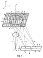
- Fig. 1 is a tangential cross-sectional view of a small part of an optical record carrier 1 having a radiation-reflecting information plane 2.
- This Figure shows one of the tracks 3 situated in the information plane 2.
- Such a track comprises information areas 3a alternating with intermediate areas 3b, whilst, for example the areas 3a are located at a height differing from that of the intermediate areas 3b.
- the information surface is scanned by a beam b emitted by a radiation source 4, for example a diode laser.
- This beam is focussed by an objective system 6 diagrammatically represented by a single lens, to form a tiny radiation spot V in the information plane.
- a separate collimator lens may be arranged ahead of the objective system.
- the imaging system may be alternatively formed by a combined collimator-objective system as is shown in Fig.1.
- a track 3 is scanned and the read beam is modulated by the information contained in this track.
- the record carrier and the read unit comprising the source 4, the objective system 6 and the detection system 10, in a radial direction relative to one another, the entire information surface is scanned.
- the beam which has been reflected and modulated by the information surface should be detected, which means that this beam should be separated from the projected beam. Therefore the apparatus should comprise a beam-separating element.
- an objective system having a large numerical aperture For reading an information structure with minute information details, for example of the order of 1 ⁇ m, an objective system having a large numerical aperture is required. The depth of focus of such an objective system is small. Since variations in the distance between the information plane 2 and the objective system 6 may occur which are larger than the depth of focus, steps have to be taken in order to detect these variations and, in response thereto, correct the focussing.
- the apparatus may be provided with a beam splitter which splits the reflected beam into two sub-beams, and with, for example two detector pairs of which a first pair co-operates with the first sub-beam and the second pair co-operates with the second sub-beam.
- the output signals of the detectors are processed to form, inter alia, a focus-servo signal.
- beam separation and beam splitting can be effected by means of a single element, namely a transparent grating.
- This grating splits the beam which is reflected by the information surface 2 and which traverses the objective system 6 into a non-diffracted zero-order sub-beam and a plurality of first-order and higher-order sub-beams.
- the grating parameters specifically the ratio between the width of the grating strips and that of the intermediate strips and the depth and the shape of the grating grooves may be selected in such a way that a maximum quantity of radiation is incident on the detection system.
- Fig. 2 is a perspective elevational view of a first embodiment of the grating 9 and the radiation-sensitive detection system 10.
- the beam b is indicated by its cross-section at the area of the grating.
- the grating 9 comprises two sub-gratings 12 and 13 separated from each other by the line 11.
- the grating strips of the sub-gratings 12 and 13 are denoted by 14 and 15, respectively. These grating strips are separated by intermediate strips 16 and 17.
- the grating strips at the area of the bounding line 11 have the same direction and are for example, perpendicular to the bounding line.
- the average grating period p1 of the sub-grating 12 is, however, different from the average grating period p2 of the sub-grating 13.
- the angle at which the sub-beam b1 is diffracted differs from the angle at which the sub-beam b2 is diffracted. This means that in the plane of the detectors the radiation spots V1 and V2 are offset with respect to each other in the X direction.
- Radiation-sensitive detectors in the form of photodiodes 18, 19 and 20, 21 which are separated by narrow strips 22 and 23, respectively, are associated with each of the sub-beams b1 and b2. These detectors are positioned in such a way that in the case of a correct focussing of the beam b on the information surface 2 the radiation spots V1 and V2 formed by the sub-beams b1 and b2 are situated symmetrically relative to the detectors 18, 19 and 20, 21, respectively.
- Figs. 3a and 3b shows the situation in which the beam b is focussed in a plane in front of the information surface 2
- Fig. 3b relates to the situation in which the beam b is focussed in a plane behind the information surface.
- S i S18+S19+S20+S21
- S r (S18+S19)-(S20+S21)
- the two sub-gratings have a varying grating period, the variation in the period being, for example of the order of several per cent of the average grating period.
- the grating strips of the two sub-gratings are curved. These sub-gratings thus have a variable lens action. Due to the varying grating period the positions of the radiation spots V1 and V2 may be varied in a direction parallel to the optical axis 00′, hence in the Z direction by displacing the grating 9 along the bounding line 11. Aberrations in a direction perpendicular to the direction of the bounding line 11 may be minimised by the curvatures of the grating strips.
- the possibility of displacing the Z positions of the radiation spots V1 andV2 is particularly important if an integrated laser-photodiode unit is used, i.e. a component in which the diode laser and the photodiodes are arranged on one support and are therefore fixed with respect to each other and thus have a fixed mutual distance in the Z direction. This distance is subject to manufacturing tolerances and cannot be corrected during assembly of the apparatus by displacing the photodiodes with respect to the laser diode in the Z direction.
- the distance in the Z direction between the diode laser and the centres of the detector pairs is subject to manufacturing tolerances.
- a compensation therefor can also be obtained by displacing the grating 9 in the direction of the line 11.
- diffraction grating having curved grating strips as compared with a grating having straight grating strips is that the optical aberrations such as coma and astigmatism which may occur when using the last-mentioned grating can be avoided in the first-mentioned grating by taking these aberrations into account in the manufacture of this grating and adapting the curvature of the grating strips thereto.
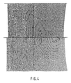
- Fig. 4 shows a part of a realised embodiment of a composite diffraction grating as can be used in the apparatus according to Fig. 1.
- the grating period varies between, for example 1.6 ⁇ m and 1.8 ⁇ m, whereas in the other sub-grating this period varies between, for example 2.4 and 2.7 ⁇ m.
- the diameter is, for example 800 ⁇ m for such a grating with a round circumference.
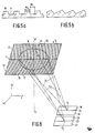
- the diffraction grating is preferably a phase grating in the form of a relief structure in which the grating grooves are located at a height which is different from that of the intermediate strips.
- the principle of such a grating is indicated in Fig. 5a.
- Such a grating can be optimised by suitable choice of the ratio between the width W1 of the grating grooves 14 and the width W2 of the intermediate strips 16 and of the depth of the grooves.
- the shape of the grooves can be adapted. Instead of the rectangular symmetrical shape shown in Fig. 5a, an asymmetrical shape is preferred, for example a sawtooth shape (Fig. 5b) because then a maximum quantity of radiation can be concentrated in one order, for example the +1 order.
- An amplitude grating or black-white grating may be used alternatively instead of a phase grating.
- This grating can be optimised by adapting the variation of the blackening.
- Both the amplitude grating and the phase grating may be copied in large numbers from a so-called master grating, the phase grating providing the advantage that it can be copied at low cost in large numbers because known pressing or replica techniques can be used which are very suitable for bulk manufacture.
- the master grating can be obtained holographically. Thereby an arrangement is used in which radiation sources emitting diverging beams are arranged in the position of the source 4 and the desired positions of the radiation spot V1 and the radiation spot V2 in Fig. 2. A photographic plate is then provided in the position of the grating 9 in Fig. 2. Firstly, one half of the plate is exposed with the beams emitted by the radiation sources in the positions of the source 4 and the spot V1, whilst the other half of the plate is shielded. Subsequently the exposed half of the plate is shielded and the other half is exposed with the beams emitted by the radiation sources in the positions of the source 4 and the radiation spot V2.
- the different interference patterns thus obtained on both halves of the plate can be converted into relief structures by means of known developing and etching techniques.
- Fig. 6 shows a second embodiment of the apparatus
- This apparatus comprises a diffraction grating whose sub-gratings have the same grating period.
- the main directions of the curved grating strips 14 of the sub-grating 12 extend at a first angle to the bounding line 11, whilst the main directions of the curved grating strips 15 of the second sub-grating 13 extend at a second, preferably equally large but opposite angle to the bounding line.
- the sub-beams are mainly deflected in a direction transversely to the main directions so that the photodiodes must be arranged differently than in Fig. 2.
- the bounding lines 22 and 23 of the detector pairs in the XY plane are now located one after the other in the Y direction.
- the focussing error signal, the information signal and the tracking error signal are obtained in the same way as described with reference to Fig. 2.
- the composite diffraction grating shown in Fig. 6 is preferred to that shown in Fig. 2.
- the sub-beams may obtain unequal intensities so that an offset in the tracking error signal may be produced. This cannot occur in an apparatus comprising the diffraction grating as shown in Fig. 6.
- the invention has been described for use in a read apparatus, but it may alternatively be used in a write apparatus or in a combined write-read apparatus in which during recording the focussing and the tracking of the write beam are monitored.
- the focus error detection system described does not utilize special properties of the information surface 2. It is merely necessary and adequate that this surface is reflecting. Therefore, the invention may be used in various apparatus where very accurate focussing is required, for example in microscopes, in which case the tracking-error detection may be dispensed with.
Abstract
Description
- The invention relates to an apparatus for optically scanning an information plane, which apparatus comprises a diode laser supplying a scanning beam, an objective system for focussing the scanning beam to form a scanning spot in the information plane, a composite diffraction grating which is arranged between the diode laser and the objective system, which grating comprises two sub-gratings for deflecting a radiation beam reflected by the information plane to a radiation-sensitive detection system comprising two detector pairs, and for splitting said radiation beam into two sub-beams each co-operating with a separate detector pair.
- An apparatus of this type which is in principle suitable for reading a prerecorded record carrier and for optically recording such a record carrier is known from United States Patent No. 4,665,310 (PHN 11.531). In this apparatus the composite diffraction grating performs two functions for which otherwise two separate elements are required. Firstly, the grating ensures that the radiation which has been reflected by the information plane and which traverses the objective system is deflected from the path of the radiation emitted by the diode laser so that a detection system can be arranged in the path of the reflected radiation. Secondly, the grating splits the reflected beam into two sub-beams required for generating a focussing error signal, i.e. a signal containing information about the magnitude and the direction of a deviation between the focal plane of the objective system and the information plane. Each of the sub-beams is associated with a separate detector pair, the signal representing the difference between the output signals of the detectors of the same pair being a measure of the focussing of the scanning beam on the information plane.
- In the said record carrier the information is arranged in accordance with information tracks. If the bounding line between the two sub-gratings extends parallel to the track direction, it is possible, by determining the sum of the output signals of each detector pair and subtracting these sum signals from each other, to form a signal containing information about the magnitude and the direction of a deviation between the centre of the scanning spot and the central axis of the information track to be scanned.
- In order to obtain the desired beam splitting the diffraction grating in the known apparatus comprises two sub-gratings having the same grating period, whilst the grating strips of the first sub-grating extend at a first angle and the grating strips of the second sub-grating extend at a second angle, which is equal but opposite to the first angle, to the bounding line of the two sub-gratings. Since a diffraction grating deflects an incident beam in a plane transversely to the direction of the grating lines, the part of the beam which is incident on one of the sub-gratings will be given a different direction than the part of the beam which is incident on the second sub-grating.
- There is an increasing need to reduce the dimensions of optical scanning apparatus for optical record carriers such as the known "CD players" so that these apparatus can be, for example, built in more easily. A reduction of the optical path length between the diode laser and the record carrier is of special importance. This length can be reduced if the distance between the diode laser and the diffraction grating can be reduced. When reducing this distance, the distance between the diffraction grating and the imaging lens system can also be reduced, whilst complying with the requirement that the parts of the diode laser beam diffraction in the first and higher orders fall outside the pupil of this lens system. When assembling the apparatus it must be possible to accurately adjust the distance, measured in a direction parallel to the optical axis of the apparatus, between the diode laser and the detectors because otherwise an offset in the focussing error signal is produced so that the scanning beam is no longer focussed on the information plane.
- In aiming at less expensive, lighter and smaller scanning apparatus it is convenient to make use of an element supplied by, for example, a semiconductor component manufacturer, which element accommodates a diode laser and detectors in the form of photodiodes, which diode laser and photodiodes are fixed with respect to each other. Due to manufacturing tolerances allowance must be made for the fact that the said distance deviates from the desired distance resulting in the offset in the focussing error signal. The influence of the said deviation will be greater as the distance between the diffraction grating and the diode laser is smaller.
- The present invention provides the possibility of compensating for the focus offset in the scanning apparatus introduced as a result of an incorrect distance between the diode laser and the photodiodes in the direction of the optical axis.
- As set forth in United States Patent No. 4,665,310 the grating design described in this patent is based on a previously proposed composite diffraction grating. This grating comprises two sub-gratings in which the grating strips of the one sub-grating have the same direction as those of the other sub-grating, but in which the grating periods of the two sub-gratings are different. In an apparatus comprising such a composite grating the two sub-beams are focussed in radiation spots located on a curve in a plane perpendicular to the plane of the detectors. Consequently, if the detector pairs are located in one plane, the two radiation spots cannot be focussed equally sharply with respect to their associated detector pair. An offset in the focussing error signal is therefore even sooner produced in this device than in a device with a composite diffraction grating in which the grating strips of the one sub-grating extend at an angle to those of the other sub-grating.
- Consequently, and also for reasons to be stated hereinafter, the present invention is eminently suitable for use in an apparatus comprising a diffraction grating which consists of two sub-gratings whose grating lines are parallel.
- The apparatus in which the present invention is used is characterized in that the diode laser and the detection system to be arranged in the apparatus are fixed with respect to each other, in that the distance measured along the optical axis of the apparatus between the diode laser and the composite grating is smaller than approximately 9 mm, in that the sub-gratings have varying grating periods and in that the grating strips of the two sub-gratings are curve.d .
- Due to the varying grating periods and the curved grating strips the composite grating has a lens action and by displacement of this grating in the direction of the bounding line between the sub-gratings, the imaging distance of the assembly of the objective system and said grating can be adapted to the distance between the diode laser and the photodiode in the direction of the optical axis.
- When using the inventive concept, it is possible to correct for imaging errors such as coma and astigmatism which may occur when using a diffraction grating with straight grating lines. To this end the curvature of the grating lines may be adapted during manufacture of the grating.
- A first embodiment of the apparatus according to the invention is further characterized in that the grating strips of the two sub-gratings at the area of the bounding line between the two sub-gratings are perpendicular to said bounding line and in that corresponding parts of the sub-gratings have different grating periods and different curva tures of the grating strips. The sub-gratings thus have a different focal power.
- A preferred embodiment of the apparatus is, however, further characterized in that corresponding parts of the sub-gratings have equal grating periods and in that the corresponding strips of the sub-gratings extend at equal but opposite angles to the bounding line between the sub-gratings.
- As compared with the first embodiment, this embodiment has the advantages mentioned in United States Patent no.4,665,310.
- A diffraction grating with curved grating strips is also referred to as a hologram in the literature. It is to be noted that in a published lecture by the Firm of NEC (Japan) entitled "An optical head using a multi-functioning hologram for CD players", which lecture was held at the "Optical Memory Symposium" in Japan on 18 December 1986, the use of a hologram in an optical read apparatus is described. This hologram performs three functions:
- separating the diode laser beam and the beam reflected by the record carrier,
- splitting the latter beam into two sub-beams for focus-error detection, and
- providing the possibility of generating a tracking-error signal. - This hologram comprises two sub-holograms deflecting the incident parts of the beam into different directions. The said publication does not state the problems for which the present invention provides a solution, which is plausible because the axial distance between the diode laser and the hologram is 18 mm. Reference is only made to possible influences which the variation of the diode laser wavelength caused by temperature variations may have on the quality of the radiation spots formed in the detector plane. The composite hologram is stated to have a focal power of substantially zero. In addition the publication states that during assembly the position of the photodiodes is adapted to the variation of the laser beam wavelength. In the schematic representation according to Fig. 1 of the publication the slanting lines in the holograms should be assumed to be shadings defining the two sub-holograms.
- According to a further characteristic feature of the apparatus the composite diffraction grating is a phase grating having a relief structure. Such a grating has a considerably higher efficiency in the desired deflection direction than an amplitude grating and provides the additional advantage that, starting from a master grating, a large number of replicas can be manufactured in known manner at low cost, which is particularly important when using the gratings in consumer apparatus.
- The invention will now be described in greater detail by way of example with reference to the accompanying drawing in which
- Fig. 1 shows diagrammatically an embodiment of a read apparatus with a diffraction grating,
- Fig. 2 is a perspective diagrammatical view of a first embodiment of the diffraction grating according to the invention and the associated radiation-sensitive detection system,
- Figs. 3a and 3b show the variations of the radiation spots on the detectors upon the occurrence of focussing errors,
- Fig. 4 shows a realised grating of the type according to Fig. 2,
- Fig. 5 shows a known diffraction grating in a cross-section and
- Fig. 6 shows a second embodiment of the diffraction grating according to the invention and the associated radiation-sensitive detection system.
- Fig. 1 is a tangential cross-sectional view of a small part of an
optical record carrier 1 having a radiation-reflectinginformation plane 2. This Figure shows one of thetracks 3 situated in theinformation plane 2. Such a track comprisesinformation areas 3a alternating withintermediate areas 3b, whilst, for example theareas 3a are located at a height differing from that of theintermediate areas 3b. The information surface is scanned by a beam b emitted by aradiation source 4, for example a diode laser. This beam is focussed by anobjective system 6 diagrammatically represented by a single lens, to form a tiny radiation spot V in the information plane. A separate collimator lens may be arranged ahead of the objective system. The imaging system may be alternatively formed by a combined collimator-objective system as is shown in Fig.1. As the record carrier is rotated about an axis 8, atrack 3 is scanned and the read beam is modulated by the information contained in this track. By moving the record carrier and the read unit, comprising thesource 4, theobjective system 6 and thedetection system 10, in a radial direction relative to one another, the entire information surface is scanned. - The beam which has been reflected and modulated by the information surface should be detected, which means that this beam should be separated from the projected beam. Therefore the apparatus should comprise a beam-separating element.
- For reading an information structure with minute information details, for example of the order of 1 µm, an objective system having a large numerical aperture is required. The depth of focus of such an objective system is small. Since variations in the distance between the
information plane 2 and theobjective system 6 may occur which are larger than the depth of focus, steps have to be taken in order to detect these variations and, in response thereto, correct the focussing. To this end the apparatus may be provided with a beam splitter which splits the reflected beam into two sub-beams, and with, for example two detector pairs of which a first pair co-operates with the first sub-beam and the second pair co-operates with the second sub-beam. The output signals of the detectors are processed to form, inter alia, a focus-servo signal. - As described in the article "Optische Fokusfehlerdetektion" in "Neues aus der Technik" no. 6, 15 December 1980,
page 3, beam separation and beam splitting can be effected by means of a single element, namely a transparent grating. This grating splits the beam which is reflected by theinformation surface 2 and which traverses theobjective system 6 into a non-diffracted zero-order sub-beam and a plurality of first-order and higher-order sub-beams. The grating parameters, specifically the ratio between the width of the grating strips and that of the intermediate strips and the depth and the shape of the grating grooves may be selected in such a way that a maximum quantity of radiation is incident on the detection system. - Fig. 2 is a perspective elevational view of a first embodiment of the grating 9 and the radiation-
sensitive detection system 10. The beam b is indicated by its cross-section at the area of the grating. The grating 9 comprises twosub-gratings line 11. The grating strips of the sub-gratings 12 and 13 are denoted by 14 and 15, respectively. These grating strips are separated byintermediate strips bounding line 11 have the same direction and are for example, perpendicular to the bounding line. The average grating period p₁ of the sub-grating 12 is, however, different from the average grating period p₂ of the sub-grating 13. Consequently, the angle at which the sub-beam b₁ is diffracted differs from the angle at which the sub-beam b₂ is diffracted. This means that in the plane of the detectors the radiation spots V₁ and V₂ are offset with respect to each other in the X direction. - Radiation-sensitive detectors in the form of
photodiodes narrow strips information surface 2 the radiation spots V₁ and V₂ formed by the sub-beams b₁ and b₂ are situated symmetrically relative to thedetectors information surface 2, whereas Fig. 3b relates to the situation in which the beam b is focussed in a plane behind the information surface. - If the output signals of the
detectors
Sf = (S₁₈+S₂₁)-(S₁₉+S₂₀)
A signal which is proportional to the information being read, or the information signal Si, is given by:
Si = S₁₈+S₁₉+S₂₀+S₂₁
If thebounding line 11 of the two sub-gratings 12 and 13 extends parallel to the direction of atrack 3 being read, it is also possible to generate a tracking error signal Sr from the detector signals. This signal is given by :
Sr = (S₁₈+S₁₉)-(S₂₀+S₂₁)
- According to the invention the two sub-gratings have a varying grating period, the variation in the period being, for example of the order of several per cent of the average grating period. Moreover, as shown in Fig. 2, the grating strips of the two sub-gratings are curved. These sub-gratings thus have a variable lens action. Due to the varying grating period the positions of the radiation spots V₁ and V₂ may be varied in a direction parallel to the optical axis 00′, hence in the Z direction by displacing the grating 9 along the bounding
line 11. Aberrations in a direction perpendicular to the direction of thebounding line 11 may be minimised by the curvatures of the grating strips. The possibility of displacing the Z positions of the radiation spots V₁ andV₂ is particularly important if an integrated laser-photodiode unit is used, i.e. a component in which the diode laser and the photodiodes are arranged on one support and are therefore fixed with respect to each other and thus have a fixed mutual distance in the Z direction. This distance is subject to manufacturing tolerances and cannot be corrected during assembly of the apparatus by displacing the photodiodes with respect to the laser diode in the Z direction. - Also the distance in the Z direction between the diode laser and the centres of the detector pairs is subject to manufacturing tolerances. A compensation therefor can also be obtained by displacing the grating 9 in the direction of the
line 11. - In the embodiment according to Fig. 2 it can be ensured that, in spite of the different angles at which the sub-beams b₁ and b₂ are deflected in the XZ plane due to the different average grating periods of the sub-gratings 12 and 13, the foci of the sub-beams are in one XY plane, namely by giving the grating periods and the curvatures of the grating strips of corresponding parts of the sub-gratings a different variation.
- An important advantage of the diffraction grating having curved grating strips as compared with a grating having straight grating strips is that the optical aberrations such as coma and astigmatism which may occur when using the last-mentioned grating can be avoided in the first-mentioned grating by taking these aberrations into account in the manufacture of this grating and adapting the curvature of the grating strips thereto.
- Fig. 4 shows a part of a realised embodiment of a composite diffraction grating as can be used in the apparatus according to Fig. 1. In one of the sub-gratings the grating period varies between, for example 1.6 µm and 1.8 µm, whereas in the other sub-grating this period varies between, for example 2.4 and 2.7 µm. The diameter is, for example 800 µm for such a grating with a round circumference.
- The diffraction grating is preferably a phase grating in the form of a relief structure in which the grating grooves are located at a height which is different from that of the intermediate strips. The principle of such a grating is indicated in Fig. 5a. Such a grating can be optimised by suitable choice of the ratio between the width W₁ of the
grating grooves 14 and the width W₂ of theintermediate strips 16 and of the depth of the grooves. In addition the shape of the grooves can be adapted. Instead of the rectangular symmetrical shape shown in Fig. 5a, an asymmetrical shape is preferred, for example a sawtooth shape (Fig. 5b) because then a maximum quantity of radiation can be concentrated in one order, for example the +1 order. - An amplitude grating or black-white grating may be used alternatively instead of a phase grating. This grating can be optimised by adapting the variation of the blackening.
- Both the amplitude grating and the phase grating may be copied in large numbers from a so-called master grating, the phase grating providing the advantage that it can be copied at low cost in large numbers because known pressing or replica techniques can be used which are very suitable for bulk manufacture.
- The master grating can be obtained holographically. Thereby an arrangement is used in which radiation sources emitting diverging beams are arranged in the position of the
source 4 and the desired positions of the radiation spot V₁ and the radiation spot V₂ in Fig. 2. A photographic plate is then provided in the position of the grating 9 in Fig. 2. Firstly, one half of the plate is exposed with the beams emitted by the radiation sources in the positions of thesource 4 and the spot V₁, whilst the other half of the plate is shielded. Subsequently the exposed half of the plate is shielded and the other half is exposed with the beams emitted by the radiation sources in the positions of thesource 4 and the radiation spot V₂. The different interference patterns thus obtained on both halves of the plate can be converted into relief structures by means of known developing and etching techniques. - Given the positions of the
radiation source 4, the diffraction grating 9 and the photodiodes, it is alternatively possible to calculate the patterns of the sub-gratings and subsequently write these patterns in an electron-sensitive material by means of, for example, an electron beam write apparatus. - Fig. 6 shows a second embodiment of the apparatus This apparatus comprises a diffraction grating whose sub-gratings have the same grating period. The main directions of the curved grating strips 14 of the sub-grating 12 extend at a first angle to the
bounding line 11, whilst the main directions of the curved grating strips 15 of thesecond sub-grating 13 extend at a second, preferably equally large but opposite angle to the bounding line. The sub-beams are mainly deflected in a direction transversely to the main directions so that the photodiodes must be arranged differently than in Fig. 2. The bounding lines 22 and 23 of the detector pairs in the XY plane are now located one after the other in the Y direction. The focussing error signal, the information signal and the tracking error signal are obtained in the same way as described with reference to Fig. 2. - Since the efficiency of a diffraction grating, i.e. the quotient of the quantity of radiation diffraction in the desired direction and the total quantity of radiation incident on the grating depends on, inter alia, the grating period, the composite diffraction grating shown in Fig. 6 is preferred to that shown in Fig. 2. In fact, due to the unequal grating periods of the sub-gratings in the last-mentioned gratings the sub-beams may obtain unequal intensities so that an offset in the tracking error signal may be produced. This cannot occur in an apparatus comprising the diffraction grating as shown in Fig. 6.
- The invention has been described for use in a read apparatus, but it may alternatively be used in a write apparatus or in a combined write-read apparatus in which during recording the focussing and the tracking of the write beam are monitored. The focus error detection system described does not utilize special properties of the
information surface 2. It is merely necessary and adequate that this surface is reflecting. Therefore, the invention may be used in various apparatus where very accurate focussing is required, for example in microscopes, in which case the tracking-error detection may be dispensed with.
Claims (4)
Applications Claiming Priority (2)
| Application Number | Priority Date | Filing Date | Title |
|---|---|---|---|
| NL8701749 | 1987-07-24 | ||
| NL8701749A NL8701749A (en) | 1987-07-24 | 1987-07-24 | DEVICE FOR SCANNING AN INFORMATION SHEET WITH OPTICAL RADIATION. |
Publications (2)
| Publication Number | Publication Date |
|---|---|
| EP0300570A1 true EP0300570A1 (en) | 1989-01-25 |
| EP0300570B1 EP0300570B1 (en) | 1992-10-14 |
Family
ID=19850368
Family Applications (1)
| Application Number | Title | Priority Date | Filing Date |
|---|---|---|---|
| EP88201516A Expired - Lifetime EP0300570B1 (en) | 1987-07-24 | 1988-07-14 | Apparatus for optically scanning an information plane |
Country Status (14)
| Country | Link |
|---|---|
| US (1) | US4829506A (en) |
| EP (1) | EP0300570B1 (en) |
| JP (1) | JP2683918B2 (en) |
| KR (1) | KR970005985B1 (en) |
| CN (1) | CN1015842B (en) |
| AT (1) | ATE81560T1 (en) |
| AU (1) | AU602646B2 (en) |
| CZ (1) | CZ280821B6 (en) |
| DE (1) | DE3875294T2 (en) |
| ES (1) | ES2036255T3 (en) |
| HK (1) | HK147095A (en) |
| NL (1) | NL8701749A (en) |
| SG (1) | SG28345G (en) |
| SK (1) | SK278407B6 (en) |
Cited By (7)
| Publication number | Priority date | Publication date | Assignee | Title |
|---|---|---|---|---|
| EP0369510A1 (en) * | 1988-11-03 | 1990-05-23 | Koninklijke Philips Electronics N.V. | Apparatus for optically scanning a radiation-reflecting information plane |
| EP0373699A1 (en) * | 1988-12-13 | 1990-06-20 | Koninklijke Philips Electronics N.V. | Optical scanning device, mirror objective suitable for use in said device and optical write and/or read apparatus provided with said device |
| EP0373700A1 (en) * | 1988-12-13 | 1990-06-20 | Koninklijke Philips Electronics N.V. | Optical scanning device, and mirror objective suitable for use in said device. |
| EP0453323A2 (en) * | 1990-04-20 | 1991-10-23 | Sharp Kabushiki Kaisha | Optical pickup device |
| EP0583036A2 (en) * | 1992-08-12 | 1994-02-16 | Koninklijke Philips Electronics N.V. | Device for optically scanning a surface |
| US5579298A (en) * | 1992-08-12 | 1996-11-26 | U.S. Philips Corporation | Optical scanner having symmetry about an oblique divider |
| EP1109163A2 (en) * | 1999-12-16 | 2001-06-20 | Victor Company Of Japan, Ltd. | Optical device |
Families Citing this family (21)
| Publication number | Priority date | Publication date | Assignee | Title |
|---|---|---|---|---|
| EP0539354B1 (en) * | 1987-08-24 | 1997-06-04 | Sharp Kabushiki Kaisha | Optical pickup apparatus |
| US4907847A (en) * | 1987-09-28 | 1990-03-13 | Nec Home Electronics Ltd. | Optical pickup and hologram therefor |
| US5066138A (en) * | 1988-06-16 | 1991-11-19 | Mitsubishi Denki Kabushiki Kaisha | Optical head apparatus |
| US4993789A (en) * | 1988-09-15 | 1991-02-19 | Jonathan R. Biles | Dual wavelength polarization selective holographic optical element |
| US5511050A (en) * | 1988-09-21 | 1996-04-23 | Hitachi, Ltd. | Focus error detecting method and optical head using the same |
| US5049732A (en) * | 1988-10-21 | 1991-09-17 | Sharp Kabushiki Kaisha | Optical pickup device with diffraction device |
| JPH06103543B2 (en) * | 1988-12-31 | 1994-12-14 | 三星電子株式会社 | Laser pickup |
| FR2646245B1 (en) * | 1989-04-25 | 1991-06-14 | Thomson Csf | OPTICAL READING DEVICE FOR OPTICAL RECORDING MEDIUM |
| US5490133A (en) * | 1990-10-05 | 1996-02-06 | Hitachi, Ltd. | Optical information processing apparatus and method of controlling position of optical spot and reproducing signals |
| JP2865223B2 (en) * | 1990-12-28 | 1999-03-08 | 松下電子工業株式会社 | Polarizing plate for optical pickup and optical pickup device |
| JPH0659717B2 (en) * | 1991-02-27 | 1994-08-10 | 株式会社淀川製鋼所 | Coated surface treated metal plate |
| DE59409779D1 (en) * | 1993-04-16 | 2001-07-19 | Infineon Technologies Ag | Diffractive optical device for the optical imaging of a spatial point on other spatial points |
| JPH1064104A (en) * | 1996-08-21 | 1998-03-06 | Pioneer Electron Corp | Astigmatic focus error signal generating method and optical pickup device |
| JPH10172170A (en) * | 1996-10-09 | 1998-06-26 | Sanyo Electric Co Ltd | Optical pickup device and its production |
| JPH10333025A (en) * | 1997-05-28 | 1998-12-18 | Pioneer Electron Corp | Optical pickup device |
| WO2000017867A1 (en) | 1998-09-21 | 2000-03-30 | Koninklijke Philips Electronics N.V. | Device for scanning an optical record carrier having at least two information layers |
| KR100456403B1 (en) | 2000-04-21 | 2004-11-10 | 제이에프이 스틸 가부시키가이샤 | Surface treated steel plate and method for production thereof |
| CN1255791C (en) * | 2000-10-03 | 2006-05-10 | 皇家菲利浦电子有限公司 | Optical scanning device |
| JP4160503B2 (en) | 2001-08-16 | 2008-10-01 | エヌエックスピー ビー ヴィ | Differential ring oscillator stage |
| CN103868889B (en) * | 2012-12-18 | 2017-02-15 | 中国科学技术大学 | Micro cantilever beam array biochemical sensing device based on micro-mirror scanning and method |
| CN110033792B (en) * | 2019-03-29 | 2020-12-04 | 华韵文化科技有限公司 | Non-contact distance measuring type old record device |
Citations (3)
| Publication number | Priority date | Publication date | Assignee | Title |
|---|---|---|---|---|
| DE3522849A1 (en) * | 1984-06-27 | 1986-01-02 | Canon Denshi K.K., Chichibu, Saitama | OPTICAL HEAD |
| US4665310A (en) * | 1985-10-17 | 1987-05-12 | U.S. Philips Corporation | Apparatus for optically scanning an information plane wherein a diffraction grating splits the beam into two sub-beams |
| EP0228620A2 (en) * | 1985-12-10 | 1987-07-15 | Nec Corporation | Optical head comprising a diffraction grating for directing two or more diffracted beams to optical detectors |
Family Cites Families (5)
| Publication number | Priority date | Publication date | Assignee | Title |
|---|---|---|---|---|
| US3272917A (en) * | 1964-02-11 | 1966-09-13 | Gen Electric | First and second order diffraction color projection system |
| US3861784A (en) * | 1973-06-29 | 1975-01-21 | Sperry Rand Corp | Programmable diffraction grating |
| JPS58220248A (en) * | 1982-06-15 | 1983-12-21 | Nippon Kogaku Kk <Nikon> | Optical pickup |
| JPS61273749A (en) * | 1985-05-29 | 1986-12-04 | Pioneer Electronic Corp | Optical pickup device |
| US4731772A (en) * | 1986-05-06 | 1988-03-15 | Lee Wai Hon | Optical head using hologram lens for both beam splitting and focus error detection functions |
-
1987
- 1987-07-24 NL NL8701749A patent/NL8701749A/en not_active Application Discontinuation
- 1987-11-04 US US07/117,006 patent/US4829506A/en not_active Expired - Lifetime
-
1988
- 1988-07-14 AT AT88201516T patent/ATE81560T1/en not_active IP Right Cessation
- 1988-07-14 ES ES198888201516T patent/ES2036255T3/en not_active Expired - Lifetime
- 1988-07-14 SG SG1995904157A patent/SG28345G/en unknown
- 1988-07-14 DE DE8888201516T patent/DE3875294T2/en not_active Expired - Fee Related
- 1988-07-14 EP EP88201516A patent/EP0300570B1/en not_active Expired - Lifetime
- 1988-07-18 JP JP63178914A patent/JP2683918B2/en not_active Expired - Fee Related
- 1988-07-21 CN CN88104607A patent/CN1015842B/en not_active Expired
- 1988-07-21 KR KR1019880009113A patent/KR970005985B1/en not_active IP Right Cessation
- 1988-07-22 AU AU19746/88A patent/AU602646B2/en not_active Ceased
- 1988-07-22 CZ CS885252A patent/CZ280821B6/en not_active IP Right Cessation
- 1988-07-22 SK SK5252-88A patent/SK278407B6/en unknown
-
1995
- 1995-09-14 HK HK147095A patent/HK147095A/en not_active IP Right Cessation
Patent Citations (3)
| Publication number | Priority date | Publication date | Assignee | Title |
|---|---|---|---|---|
| DE3522849A1 (en) * | 1984-06-27 | 1986-01-02 | Canon Denshi K.K., Chichibu, Saitama | OPTICAL HEAD |
| US4665310A (en) * | 1985-10-17 | 1987-05-12 | U.S. Philips Corporation | Apparatus for optically scanning an information plane wherein a diffraction grating splits the beam into two sub-beams |
| EP0228620A2 (en) * | 1985-12-10 | 1987-07-15 | Nec Corporation | Optical head comprising a diffraction grating for directing two or more diffracted beams to optical detectors |
Non-Patent Citations (3)
| Title |
|---|
| OPTICAL MEMORY NEWS, Nr. 31, Januar 1986, Seite 18, Rothchild Consultants, San Francisco, CA, US; S. URA et al.: "An integrated optic disck pickup device" * |
| OPTICAL MEMORY SYMPOSIUM, Tokyo, 18. Dezember 1986, Seiten 93-98; Y. KIMURA et al.: "An optical head using a multi-functional hologram for CD-players" * |
| TOPICAL MEETING ON OPTICAL DATA STORAGE, Stateline, Nevada, 11.-13. März 1987, Optical Society of America, Washington, DC, US; Y. KIMURA et al.: "A compact optical head using holographic optical element for CD players" * |
Cited By (11)
| Publication number | Priority date | Publication date | Assignee | Title |
|---|---|---|---|---|
| EP0369510A1 (en) * | 1988-11-03 | 1990-05-23 | Koninklijke Philips Electronics N.V. | Apparatus for optically scanning a radiation-reflecting information plane |
| EP0373699A1 (en) * | 1988-12-13 | 1990-06-20 | Koninklijke Philips Electronics N.V. | Optical scanning device, mirror objective suitable for use in said device and optical write and/or read apparatus provided with said device |
| EP0373700A1 (en) * | 1988-12-13 | 1990-06-20 | Koninklijke Philips Electronics N.V. | Optical scanning device, and mirror objective suitable for use in said device. |
| EP0453323A2 (en) * | 1990-04-20 | 1991-10-23 | Sharp Kabushiki Kaisha | Optical pickup device |
| EP0453323B1 (en) * | 1990-04-20 | 1995-12-13 | Sharp Kabushiki Kaisha | Optical pickup device |
| EP0583036A2 (en) * | 1992-08-12 | 1994-02-16 | Koninklijke Philips Electronics N.V. | Device for optically scanning a surface |
| EP0583036A3 (en) * | 1992-08-12 | 1994-04-20 | Koninklijke Philips Electronics N.V. | Device for optically scanning a surface |
| US5579298A (en) * | 1992-08-12 | 1996-11-26 | U.S. Philips Corporation | Optical scanner having symmetry about an oblique divider |
| EP1109163A2 (en) * | 1999-12-16 | 2001-06-20 | Victor Company Of Japan, Ltd. | Optical device |
| EP1109163A3 (en) * | 1999-12-16 | 2003-07-09 | Victor Company Of Japan, Ltd. | Optical device |
| US6891675B2 (en) | 1999-12-16 | 2005-05-10 | Victor Company Of Japan, Limited | Optical device |
Also Published As
| Publication number | Publication date |
|---|---|
| JPS6453353A (en) | 1989-03-01 |
| HK147095A (en) | 1995-09-22 |
| NL8701749A (en) | 1989-02-16 |
| AU602646B2 (en) | 1990-10-18 |
| ATE81560T1 (en) | 1992-10-15 |
| JP2683918B2 (en) | 1997-12-03 |
| CN1030987A (en) | 1989-02-08 |
| KR970005985B1 (en) | 1997-04-22 |
| DE3875294D1 (en) | 1992-11-19 |
| CN1015842B (en) | 1992-03-11 |
| DE3875294T2 (en) | 1993-04-29 |
| US4829506A (en) | 1989-05-09 |
| KR890002848A (en) | 1989-04-11 |
| SG28345G (en) | 1995-09-18 |
| CZ280821B6 (en) | 1996-04-17 |
| AU1974688A (en) | 1989-01-27 |
| ES2036255T3 (en) | 1993-05-16 |
| SK278407B6 (en) | 1997-04-09 |
| EP0300570B1 (en) | 1992-10-14 |
Similar Documents
| Publication | Publication Date | Title |
|---|---|---|
| EP0300570B1 (en) | Apparatus for optically scanning an information plane | |
| US4665310A (en) | Apparatus for optically scanning an information plane wherein a diffraction grating splits the beam into two sub-beams | |
| US5391865A (en) | Optical pickup apparatus and optical grating assembly therefor | |
| EP0219170B1 (en) | Apparatus for reading and/or recording a trackwise arranged optical information structure | |
| EP0372629A2 (en) | Apparatus for optically scanning an information plane | |
| JPH0758559B2 (en) | Optical pickup device | |
| EP0308022B1 (en) | Apparatus for optically scanning a radiation-reflective information plane | |
| JP2684822B2 (en) | Optical pickup head device | |
| US4771411A (en) | Device for scanning a radiation-reflecting information surface with optical radiation | |
| US4908506A (en) | Apparatus for optically scanning a radiation-reflecting information plane | |
| EP0509526B1 (en) | Optical pickup head | |
| JPH04364231A (en) | Optical head device | |
| US5018804A (en) | Laser pick-up | |
| US5648946A (en) | Optical pick-up apparatus with holographic optical element to diffract both forward and return light beams | |
| US7298676B2 (en) | Optical pickup apparatus having optical detection area for compensating for tracking error offset | |
| EP0475523B1 (en) | Device for optically scanning an information plane | |
| JPH1139676A (en) | Sensor system for optical disk | |
| JPH09282683A (en) | Optical device | |
| US20070247984A1 (en) | Optical Record Carrier and Optical Scanning Device | |
| JPH0792929B2 (en) | Optical pickup device | |
| JPH0648544B2 (en) | Optical pickup high density recording information reproducing device | |
| JPH07192306A (en) | Optical pickup | |
| JPH052762A (en) | Optical recording and reproducing device |
Legal Events
| Date | Code | Title | Description |
|---|---|---|---|
| PUAI | Public reference made under article 153(3) epc to a published international application that has entered the european phase |
Free format text: ORIGINAL CODE: 0009012 |
|
| AK | Designated contracting states |
Kind code of ref document: A1 Designated state(s): AT BE DE ES FR GB IT NL SE |
|
| 17P | Request for examination filed |
Effective date: 19890715 |
|
| 17Q | First examination report despatched |
Effective date: 19911127 |
|
| GRAA | (expected) grant |
Free format text: ORIGINAL CODE: 0009210 |
|
| AK | Designated contracting states |
Kind code of ref document: B1 Designated state(s): AT BE DE ES FR GB IT NL SE |
|
| PG25 | Lapsed in a contracting state [announced via postgrant information from national office to epo] |
Ref country code: SE Effective date: 19921014 Ref country code: NL Effective date: 19921014 |
|
| REF | Corresponds to: |
Ref document number: 81560 Country of ref document: AT Date of ref document: 19921015 Kind code of ref document: T |
|
| REF | Corresponds to: |
Ref document number: 3875294 Country of ref document: DE Date of ref document: 19921119 |
|
| ITF | It: translation for a ep patent filed |
Owner name: ING. C. GREGORJ S.P.A. |
|
| ET | Fr: translation filed | ||
| NLV1 | Nl: lapsed or annulled due to failure to fulfill the requirements of art. 29p and 29m of the patents act | ||
| PLBE | No opposition filed within time limit |
Free format text: ORIGINAL CODE: 0009261 |
|
| STAA | Information on the status of an ep patent application or granted ep patent |
Free format text: STATUS: NO OPPOSITION FILED WITHIN TIME LIMIT |
|
| 26N | No opposition filed | ||
| ITPR | It: changes in ownership of a european patent |
Owner name: CAMBIO RAGIONE SOCIALE;PHILIPS ELECTRONICS N.V. |
|
| REG | Reference to a national code |
Ref country code: FR Ref legal event code: CD |
|
| REG | Reference to a national code |
Ref country code: ES Ref legal event code: PC2A Owner name: PHILIPS ELECTRONICS N.V. |
|
| REG | Reference to a national code |
Ref country code: FR Ref legal event code: CD |
|
| REG | Reference to a national code |
Ref country code: ES Ref legal event code: PC2A |
|
| REG | Reference to a national code |
Ref country code: GB Ref legal event code: IF02 |
|
| PGFP | Annual fee paid to national office [announced via postgrant information from national office to epo] |
Ref country code: BE Payment date: 20040621 Year of fee payment: 17 |
|
| PGFP | Annual fee paid to national office [announced via postgrant information from national office to epo] |
Ref country code: ES Payment date: 20040707 Year of fee payment: 17 |
|
| PGFP | Annual fee paid to national office [announced via postgrant information from national office to epo] |
Ref country code: FR Payment date: 20040727 Year of fee payment: 17 |
|
| PGFP | Annual fee paid to national office [announced via postgrant information from national office to epo] |
Ref country code: AT Payment date: 20040728 Year of fee payment: 17 |
|
| PGFP | Annual fee paid to national office [announced via postgrant information from national office to epo] |
Ref country code: GB Payment date: 20040729 Year of fee payment: 17 |
|
| PGFP | Annual fee paid to national office [announced via postgrant information from national office to epo] |
Ref country code: DE Payment date: 20040916 Year of fee payment: 17 |
|
| PG25 | Lapsed in a contracting state [announced via postgrant information from national office to epo] |
Ref country code: IT Free format text: LAPSE BECAUSE OF NON-PAYMENT OF DUE FEES;WARNING: LAPSES OF ITALIAN PATENTS WITH EFFECTIVE DATE BEFORE 2007 MAY HAVE OCCURRED AT ANY TIME BEFORE 2007. THE CORRECT EFFECTIVE DATE MAY BE DIFFERENT FROM THE ONE RECORDED. Effective date: 20050714 Ref country code: GB Free format text: LAPSE BECAUSE OF NON-PAYMENT OF DUE FEES Effective date: 20050714 Ref country code: AT Free format text: LAPSE BECAUSE OF NON-PAYMENT OF DUE FEES Effective date: 20050714 |
|
| PG25 | Lapsed in a contracting state [announced via postgrant information from national office to epo] |
Ref country code: ES Free format text: LAPSE BECAUSE OF NON-PAYMENT OF DUE FEES Effective date: 20050715 |
|
| PG25 | Lapsed in a contracting state [announced via postgrant information from national office to epo] |
Ref country code: BE Free format text: LAPSE BECAUSE OF NON-PAYMENT OF DUE FEES Effective date: 20050731 |
|
| PG25 | Lapsed in a contracting state [announced via postgrant information from national office to epo] |
Ref country code: DE Free format text: LAPSE BECAUSE OF NON-PAYMENT OF DUE FEES Effective date: 20060201 |
|
| GBPC | Gb: european patent ceased through non-payment of renewal fee |
Effective date: 20050714 |
|
| PG25 | Lapsed in a contracting state [announced via postgrant information from national office to epo] |
Ref country code: FR Free format text: LAPSE BECAUSE OF NON-PAYMENT OF DUE FEES Effective date: 20060331 |
|
| REG | Reference to a national code |
Ref country code: FR Ref legal event code: ST Effective date: 20060331 |
|
| REG | Reference to a national code |
Ref country code: ES Ref legal event code: FD2A Effective date: 20050715 |
|
| BERE | Be: lapsed |
Owner name: *KONINKLIJKE PHILIPS ELECTRONICS N.V. Effective date: 20050731 |