EP0300224B1 - Strainless precision after-treatment process by radical reaction - Google Patents
Strainless precision after-treatment process by radical reaction Download PDFInfo
- Publication number
- EP0300224B1 EP0300224B1 EP88110108A EP88110108A EP0300224B1 EP 0300224 B1 EP0300224 B1 EP 0300224B1 EP 88110108 A EP88110108 A EP 88110108A EP 88110108 A EP88110108 A EP 88110108A EP 0300224 B1 EP0300224 B1 EP 0300224B1
- Authority
- EP
- European Patent Office
- Prior art keywords
- workpiece
- electrode
- strainless
- radical reaction
- precision process
- Prior art date
- Legal status (The legal status is an assumption and is not a legal conclusion. Google has not performed a legal analysis and makes no representation as to the accuracy of the status listed.)
- Expired - Lifetime
Links
Images

Classifications
-
- B—PERFORMING OPERATIONS; TRANSPORTING
- B28—WORKING CEMENT, CLAY, OR STONE
- B28D—WORKING STONE OR STONE-LIKE MATERIALS
- B28D5/00—Fine working of gems, jewels, crystals, e.g. of semiconductor material; apparatus or devices therefor
-
- C—CHEMISTRY; METALLURGY
- C30—CRYSTAL GROWTH
- C30B—SINGLE-CRYSTAL GROWTH; UNIDIRECTIONAL SOLIDIFICATION OF EUTECTIC MATERIAL OR UNIDIRECTIONAL DEMIXING OF EUTECTOID MATERIAL; REFINING BY ZONE-MELTING OF MATERIAL; PRODUCTION OF A HOMOGENEOUS POLYCRYSTALLINE MATERIAL WITH DEFINED STRUCTURE; SINGLE CRYSTALS OR HOMOGENEOUS POLYCRYSTALLINE MATERIAL WITH DEFINED STRUCTURE; AFTER-TREATMENT OF SINGLE CRYSTALS OR A HOMOGENEOUS POLYCRYSTALLINE MATERIAL WITH DEFINED STRUCTURE; APPARATUS THEREFOR
- C30B33/00—After-treatment of single crystals or homogeneous polycrystalline material with defined structure
Landscapes
- Engineering & Computer Science (AREA)
- Chemical & Material Sciences (AREA)
- Mechanical Engineering (AREA)
- Crystallography & Structural Chemistry (AREA)
- Materials Engineering (AREA)
- Metallurgy (AREA)
- Organic Chemistry (AREA)
- Electrical Discharge Machining, Electrochemical Machining, And Combined Machining (AREA)
Description
- This invention relates to a strainless precision process on radical (free radical) reaction and, more particularly, to a precision process ensuring strainless cutting, boring and grinding of brittle materials hard to work on such as silicon and germanium single crystal for manufacturing semiconductors, gallium-arsenic compound, various ceramics materials or the like.
- A prior art precision process, or cutting for example, of brittle materials hard to work on such as silicon and germanium single crystal for manufacturing semiconductors, gallium-arsenic compound, various ceramics materials or the like depends only on dicing on a diamond wheel, and since its working principle comprises a brittle fracture by fine cracking, a serviceable surface will not be secured due to residual cracks unless the cut face is removed about 100 /1.m in thickness on the average. Further, the brittle fracture due to cracks is rather probable and a considerably large crack may remain according to circumstances, which is capable of deteriorating the reliability of an obtained surface. Thus, the cut face of a workpiece must be removed at about 100 /1.m in thickness, for which lapping is employed, however, since its working principle also comprises a brittle fracture, a residual affected layer is rather deep while not so heavy as compared with the aforementioned dicing, and thus an after-treatment such as etching, polishing or the like is further required. Then, lapping is also carried out for grinding the surface of a workpiece, however, the lapping is realized by transferring the flatness of a lapping tool to the workpiece, and since it depends in this case on a brittle fracture likewise according to a conventional process using a grade, both surface roughness and surface property are not to withstand the final purpose. Further, the prior art process is that of utilizing a thermal fusion phenomenon on laser for boring, grooving and so forth, therefore a thermal affected layer or a residual crack arsing on thermal stress is present on a finished surface. Thus in the prior art process, not only a residual crack and a thermal affected layer are present on the finished surface, but also a finished portion is removed so much, therefore yield of a workpiece is high, and further a production process increases in number, thus preventing a cut in cost of semiconductors and others using expensive silicon and germanium single crystal, or gallium-arsenic compound.
- In view of the situation mentioned above, an object of the invention is to provide a strainless precision process on radical reaction, wherein defects such as residual crack, thermal affected layer and the like which are capable of deteriorating a reliability of products are not left on the surface of a workpiece, still further lapping, or a work for removing the workpiece surface at about 100 /1.m or over in thickness is not required as an after-treatment unlike the prior art process, thus not only the post-process is considerably simplified, but also the workpiece can be utilized effectively.
- In order to attain the aforementioned object, the invention provides a strainless precision process on radical reaction, which comprises activating a gas selectively by discharge or laser beam excitation in the vicinity of a workpiece disposed in a gaseous atmosphere, vaporizing a compound produced according to a radical reaction with atom or molecule constituting the workpiece, thereby processing the workpiece.
- The strainless precision process on radical reaction according to the invention as above is that in which a gas in the vicinity of a portion to work of a workpiece disposed in a gaseous atmosphere is activated selectively by discharge or laser beam excitation to generate a radical with high reactivity, a compound produced according to a reaction of the radical with atom or molecule constituting the workpiece is vaporized and thus removed from the portion to work, thereby cutting, smoothing, boring and grooving the workpiece which is hard to work.
- Other object, features and advantages of this invention will become apparent from the following description, the appended claims and the accompanying drawings.
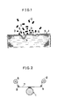
- Fig. 1 is a sectional view illustrating a principle of a strainless precision process on radical reaction according to the invention.
- Fig. 2 is a simplified sectional view showing a cutting on discharge of a wire electrode.
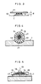
- Fig. 3 is a simplified sectional view showing a smoothing on discharge of a lapped electrode.
- Fig. 4 is a simplified sectional view showing a cutting on excitation of radiated laser beams.
- Fig. 5 is a simplified sectional view showing a smoothing on excitation of laser beams radiated evenly.
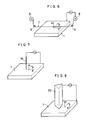
- Fig. 6 is a simplified perspective view showing cutting and grooving by means of a wire electrode as in the case of Fig. 2.
- Fig. 7 is a simplified perspective view showing a boring by means of a needle electrode.
- Fig. 8 is a simplified perspective view showing a transfer for transferring sectional form to a workpiece by means of a prismatic electrode.
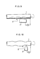
- Fig. 9 is a simplified side view showing a smoothing of the outer peripheral surface of a columnar workpiece by means of a tool-like electrode.
- Fig. 10 is a simplified side view showing a smoothing for shaping the outer peripheral surface of a workpiece symmetrically in rotation by means of a tool-like electrode.
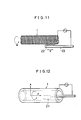
- Fig. 11 is a simplified side view showing a threading of a cylindrical workpiece by means of a sawtooth electrode.
- Fig. 12 is a simplified perspective view showing a smoothing of the inner peripheral surface of a cylindrical workpiece by means of a tool-like electrode.
- Fig. 13 is a simplified perspective view showing a smoothing for shaping the inner peripheral surface of a cylindrical workpiece symmetrically in rotation arbitrarily by means of a tool-like electrode.
- Fig. 14 is a simplified side view showing a gear cutting by means of a gear-toothed electrode.
- Fig. 15 is a simplified perspective view showing a transfer by means of a ring electrode as in the case of Fig. 8.
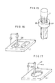
- Fig. 16 is a simplified perspective view showing a reshaping by means of a correction electrode.
- Fig. 17 is a simplified perspective view showing an arbitrary shaping by means of a rod electrode with a hemispherical surface on the nose.
- The invention comprises carrying out a strainless precision process through a radical reaction (free radical reaction) of a reactive radical (free radical) having an unpaired electron with atom or molecule constituting a workpiece.
- Here, as a method for generating a radical, it is conceivable that a plasma which can easily be produced by discharge at a degree of
vacuum high pressure 1 bar. or over in the invention, and a radical generated by DC discharge or laser beam irradiation may be used otherwise. - More specifically, the strainless precision process is carried out such that a workpiece of a brittle material hard to work such as silicon and germanium single crystal for manufacturing semiconductors, gallium-arsenic compound, various ceramics materials or the like is disposed in an atmospheric gas such as chlorine (C12), fluorine (F2) or the like, a DC voltage or high frequency voltage is impressed between a workpiece of conductor and an electrode of material relatively high in reaction temperature with a chloride gas such as tungsten (W), platinum (Pt) or the like which is disposed a little apart from the workpiece, a high frequency voltage is impressed between the aforementioned electrode and another electrode disposed in the vicinity of the work piece of insulator, a discharge is caused near the surface of the workpiece to generate a radical reactive chemically from the atmospheric gas, then a radical is generated from irradiating laser beams oscillated by solid laser, gas laser and liquid laser to the gas present near the surface of the workpiece of conductor or insulator, and in case, for example, silicon is used as the workpiece and a chloride gas is used as the gas, a radical reaction is caused on the surface of a working portion of the silicon to generate a silicon chloride, and the silicon chloride is vaporized and removed at ordinary temperature or at 200 ° C or below.
- The invention will now be described further in detail with reference to the accompanying drawings representing preferred embodiments thereof. Fig. 1 illustrates the principle of a process of the invention, wherein a
reference numeral 1 denotes a workpiece, 2 denotes a gas molecule, 3 denotes a radical (free radical), 4 denotes a constituent atom or molecule of theworkpiece 1, and 5 denotes a compound. Theradical 3 is produced by subjecting the gas molecule 2 to a discharge or laser beam excitation near the surface of theworkpiece 1 disposed in the atmospheric gas 2, the compound 5 capable of vaporizing at relatively low temperature is produced on reaction of theradical 3 with the constituent atom or molecule 4 of theworkpiece 1, the compound 5 is vaporized by warming up theworkpiece 1 to a set temperature relatively low or, for example, 200 ° C or below on ordinary temperature or heater or the like (not indicated), thus removed from the working surface to form successively aspace 6 of atom or molecule unit on theworkpiece 1 to a macro recess, thus carrying out strainless cutting, boring, grooving and so forth. Similarly in a strainless smoothing, the radical reaction may also take place most probably at a small portion projecting from the surface of theworkpiece 1, consequently the projecting portion is removed selectively to smoothing on atom or molecule level. - Fig. 2 is a principle drawing of a device for strainless cutting by means of the
radical 3 generated on a discharge of theworkpiece 1, wherein awire electrode 7 such as tungsten, platinum or the like is wound on feeding and take-upreels wire electrode 7 is laid apart a little from theworkpiece 1 through a plurality of guide rollers 9, ..., and in case theworkpiece 1 is a conductor, a discharge is generated on a DC voltage or high frequency voltage impressed by a DC power or RF (high frequency) power (not indicated) between theworkpiece 1 and thewire electrode 7 to activate the atmospheric gas 2 (not indicated), thespace 6 is produced only in an area where theradical 3 is present as shown in Fig. 1 according to a radical reaction of the generatedradical 3 with the constituent atom or molecule 4 of theworkpiece 1, and further a distance between thewire electrode 7 and theworkpiece 1 is changed relatively to cutting. Then, in case theworkpiece 1 is an insulator, a discharge is generated on a high frequency voltage impressed on thewire electrode 7 to a radical reaction likewise. Here, thewire electrode 7 normally uses a fine wire several /1.m to several ten /1.m in the precision process, therefore thereels 8 are rotated to have the wire wound on one side for feeding at all times, thereby preventing thewire electrode 7 from cutting due to a discharge at the identical portion. Further, theworkpiece 1 and thewire electrode 7 are shifted relatively on computer control or other means available, and thus a radical reaction area is changed successively to cutting of theworkpiece 1. - Fig. 3 is a principle drawing of a device for smoothing the surface of the
workpiece 1 by means of theradical 3 generated on discharge likewise, wherein a plane lappedelectrode 11 is disposed in parallel and also at a small distance d over theplane workpiece 1 fixed on asurface plate 10, a DC or high frequency voltage is impressed between the lappedelectrode 11 and theworkpiece 1 according to theworkpiece 1 being a conductor or an insulator, a discharge is thus caused to generate theradical 3, thereby removing the constituent atom or molecule 4 of theworkpiece 1. Here, the discharge is generated selectively on a point effect between the lappedelectrode 11 and theworkpiece 1 at a salient 12 present on the surface of theworkpiece 1, a removal of the constituent atom or molecule 4 on the radical reaction goes on at the portion, thus smoothing the surface of theworkpiece 1. Then, the distance d between thelapped electrode 11 and theworkpiece 1 may be optimized for gap by gap sensor or the like, thereby enhancing a working efficiency, and further the lappedelectrode 11 and theworkpiece 1 can be shifted relatively so as to minimize a damage due to discharge of thelapped electrode 11 and also to work the surface as wide as possible. Further, a curved surface of theworkpiece 1 can also be smoothed by means of the lappedelectrode 11 with a form according to the curved surface. - Still further, as shown in Fig. 4 and Fig. 5, the
radical 3 is generated from exciting optically the atmospheric gas molecule 2 bylaser beams 13 induced to a working portion of theworkpiece 1, thereby realizing a strainless precision process. In Fig. 4,optical fibers 15 are buried in adisk wheel 14 radially and peripherally from the center,incident ports 16 of thelaser beams 13 are formed intensively at the center,ejection ports 17, ... are formed outwardly on the peripheral edge portion, thelaser beams 13 are thus ready for irradiating on the gas molecule 2 present near the surface of theworkpiece 1 from a peripheral edge of thewheel 14 disposed orthogonally to the surface of theworkpiece 1, and the compound 5 produced on a radical reaction of the radial 3 generated by thelaser beams 13 with the constituent atom or molecule 4 of theworkpiece 1 is removed accordingly, thereby realizing a strainless cutting or grooving. Then, as shown in Fig. 5, theincident ports 16 of thelaser beams 13 are formed intensively on one side of aplane lap plate 18, theejection ports 17, ... are formed in dispersion uniformly at predetermined intervals on the other side opposite to theworkpiece 1, theincident ports 16 and theejection ports 17, ... are coupled optically through theoptical fibers 15, ... buried internally, thelap plate 18 is disposed a little apart from and in parallel with theworkpiece 1, thelaser beams 13 are irradiated to the gas molecule 2 near the surface of theworkpiece 1, and thus the salient 12 present on the surface of theworkpiece 1 is smoothed according to the radical reaction likewise. Here, an ejection angle of thelaser beams 13 from theejection ports 17 is large, and since a power density of thelaser beams 13 deteriorates according as the distance from thelap plate 18 gets large, the constituent atom or molecule 4 at the salient 12 which is nearest to thelap plate 18 is removed, and thus the salient 12 is smoothed selectively as a result. Then, a continuous process may be realized likewise by shifting thewheel 14 or thelap plate 18 and theworkpiece 1 relatively, and thewheel 14 is rotated to change a position for irradiating thelaser beams 13 continuously, thereby obtaining an exceedingly uniform working plane. Then, a process on radical reaction for which an optical excitation of thelaser beams 13 is utilized can be applied to various properties of theworkpiece 1 irrespective of conductor or insulator. Further, for boring and grooving, a strainless precision process may be realized likewise according to a home position irradiation and scanning of focused laser beams. - Examples of various processes from utilizing the aforementioned working principle by discharge will further be described, next.
- Fig. 6 represents a cutting method as in the case of Fig. 2, wherein the
wire electrode 7 disposed in parallel with theplane workpiece 1 is delivered in the direction X, thewire electrode 7 and theworkpiece 1 are shifted relatively in the direction Z to cut theworkpiece 1, and further shifted in the direction Y to cut or groove a new portion. Then, the cut face is flattened according to a linearity of thelaid wire electrode 7. - Fig. 7 represents a method for boring the
workpiece 1 by shiftingneedle electrode 19 kept orthogonal to theworkpiece 1 with its tip disposed to come near thereto in the direction Z, and a method for grooving by shifting theneedle electrode 19 or theworkpiece 1 in the directions X and Y is further represented therein. - Fig. 8 represents a working method or transferring method for forming a recess same in sectional form as a
prismatic electrode 20 on theworkpiece 1 by keeping the prismatic electrode 20 (triangular prism as indicated) having a predetermined sectional form orthogonal to theworkpiece 1 and shifting it in the direction Z. - Fig. 9 to Fig. 11 represent a method for working the outer peripheral surface from rotating the
workpiece 1 with a symmetrical form in rotation. Fig. 9 represents a method wherein a tool-like electrode 21 having a plane is disposed near the outer periphery of thecylindrical workpiece 1 in parallel therewith, theworkpiece 1 is rotated, the tool-like electrode 21 is shifted axially or in the direction Z and further shifted in the direction X to have the interval adjusted accordingly, thus smoothing the outer peripheral surface of theworkpiece 1, Fig. 10 represents a method wherein the outer peripheral surface of theworkpiece 1 is smoothed likewise to an arbitrary symmetrical form in rotation by means of the tool-like electrode 21 with the nose almost pointed, and further Fig. 11 represents a method wherein a saw-tooth electrode 23 havingprojections 22, ... arranged at regular intervals linearly is shifted axially at a velocity v in tune with a rotational angle speed", of theworkpiece 1, thereby threading the outer periphery of theworkpiece 1. - Fig. 12 and Fig. 13 represent a method for working the inner peripheral surface from rotating the
hollow workpiece 1 with a symmetrical form in rotation. Fig. 12 represents a method wherein the tool-like electrode 21 having a plane is disposed near the inner peripheral surface of the hollowcylindrical workpiece 1 in parallel therewith, theworkpiece 1 is rotated, the tool-like electrode 21 is shifted axially or in the direction Z and further shifted in the direction X to have the interval adjusted accordingly, thus smoothing the inner peripheral surface of theworkpiece 1, and Fig. 13 represents a method wherein the inner peripheral surface of theworkpiece 1 is smoothed likewise to an arbitrary symmetrical form in rotation by means of the tool-like electrode 21 with the nose almost pointed. - Fig. 14 represents a method wherein a gear-
toothed electrode 25 havingprojections 24, ... arranged at regular intervals on the outer periphery of a disk and thedisk workpiece 1 are disposed with each outer periphery coming near and each shaft kept in the same direction, the gear-toothed electrode 25 is rotated in one direction at an angular velocity ω1,and theworkpiece 1 is rotated reversely at an angular velocity "'2, thereby carrying out a gear-cutting on the outer periphery of theworkpiece 1. Here, a circular pitch of the gear teeth formed on theworkpiece 1 can be set properly by adjusting the angular velocities w, and "'2. - Fig. 15 represents a transfer similar to the working method shown in Fig. 8, wherein the cylindrical or
prismatic workpiece 1 disposed within aring electrode 27 with a proper shape of tongued-and-grooved face 26 necessary for working formed on the inner periphery is shifted axially, and thus a shape of the tongued-and-groovedface 26 is transferred axially on the outer peripheral surface of theworkpiece 1, thereby transferring a sectional form of thering electrode 27 to theworkpiece 1. - Fig. 16 represents a method for reshaping a working face entirely as working a predetermined margin only at each point on the working face of the
workpiece 1 by means of acorrection electrode 28 having shape and size capable of correcting a local shape of theworkpiece 1 on the nose. Then, the process corresponds to a process such as end milling or the like in a conventional milling. - Fig. 17 represents a method for working the
workpiece 1 to a complicate shape by means of arod electrode 29 with a hemispherical nose. The process corresponds to a conventional ball milling or the like. - As described, the invention comprises removing and so working the
workpiece 1 on an atom or molecule level by the radical 3 generated in the atmospheric gas 2 through discharge or laser beam excitation, and an optimum condition must be set according to a material and area to work of theworkpiece 1. In case, for example, a working is carried out on discharge, where pressure of the atmospheric gas 2 is low, the working may proceed slowly in a large area as the discharge covers an extensive range, which is suitable to smoothing, but where the pressure is high, the working may proceed efficiently and locally as the discharge is limited and thus the radical 3 may be generated at high probability, which is suitable to cutting by thewire electrode 7 and also to boring by theneedle electrode 19. Then, the atmospheric gas 2 optimized to a material of theworkpiece 1 must be selected, and further it is necessary to heat theworkpiece 1 to such temperature as will not cause a thermal denaturation according to temperature easy to cause a radical reaction of the generated radical 3 with the constituent atom or molecule 4 and also to a vaporization temperature of the compound 5 produced on the radical reaction. For example, if a silicon single crystal used best for semiconductor element material is selected as theworkpiece 1, then chloride gas is employed normally as the atmospheric gas 2, a radical reaction is caused at relatively low temperature, a sublimable silicon chloride is produced, and the silicon chloride can be vaporized at ordinary temperature or at 200 ° C or below. - According to the strainless precision process on radical reaction of the invention described as above, a gas is activated selectively on discharge or laser beam excitation in the vicinity of a workpiece disposed in a gaseous atmosphere, a compound produced on a radical reaction with a constituent atom or molecule of the workpiece is vaporized, therefore a working contactless in principle may be effected, and hence a strainless process totally freee from residual defect and thermally affected layer such as crack and the like which cannot be avoided with the prior art process using a brittle fracture by fine cracks and thus deteriorate a reliability of the working face most probably may be realized, a reliability of products can sharply be enhanced, and since the process comprises removing the workpiece on a constituent atom or molecule level, an exceedingly fine portion can be processed in precision simply in principle, and further the workpiece will never be damaged, therefore an after-treatment whereby a cut face is removed by 100 /1.m or over in thickness hitherto is no more required, and thus not only the post-process is so simplified, but also materials can be utilized effectively. While the strainless precision process according to the invention is so efficient as described above, it is quite simple that a reactive radical is generated by activating selectively a gas in the vicinity of the working portion of a workpiece disposed in a gaseous atmosphere through discharge or laser beam excitation, a compound produced on a radical reaction of the radical with an atom or molecule constituting the workpiece is vaporized spontaneously or by heating not to denature the workpiece and then removed from the working portion, thereby realizing a precision process such as strainless cutting, smoothing, boring, grooving and so forth.
Claims (11)
Applications Claiming Priority (2)
| Application Number | Priority Date | Filing Date | Title |
|---|---|---|---|
| JP160760/87 | 1987-06-26 | ||
| JP16076087 | 1987-06-26 |
Publications (4)
| Publication Number | Publication Date |
|---|---|
| EP0300224A2 EP0300224A2 (en) | 1989-01-25 |
| EP0300224A3 EP0300224A3 (en) | 1990-11-28 |
| EP0300224B1 true EP0300224B1 (en) | 1993-12-08 |
| EP0300224B2 EP0300224B2 (en) | 1998-09-30 |
Family
ID=15721874
Family Applications (1)
| Application Number | Title | Priority Date | Filing Date |
|---|---|---|---|
| EP88110108A Expired - Lifetime EP0300224B2 (en) | 1987-06-26 | 1988-06-24 | Strainless precision after-treatment process by radical reaction |
Country Status (3)
| Country | Link |
|---|---|
| US (1) | US4960495A (en) |
| EP (1) | EP0300224B2 (en) |
| DE (1) | DE3886113T3 (en) |
Families Citing this family (7)
| Publication number | Priority date | Publication date | Assignee | Title |
|---|---|---|---|---|
| US5397420A (en) * | 1991-03-03 | 1995-03-14 | Nippondenso Co., Ltd. | Fine structure forming device |
| FR2685127B1 (en) * | 1991-12-13 | 1994-02-04 | Christian Licoppe | GAS PHOTONANOGRAPH FOR THE MANUFACTURE AND OPTICAL ANALYSIS OF PATTERNS ON THE NANOMETRIC SCALE. |
| DE19518270C1 (en) * | 1995-05-18 | 1996-08-22 | Fraunhofer Ges Forschung | Non-slip polished floor covering |
| JP3069271B2 (en) * | 1995-07-12 | 2000-07-24 | 勇藏 森 | High-efficiency processing method and device using high-density radical reaction using rotating electrode |
| JPH09272119A (en) * | 1996-04-04 | 1997-10-21 | Daido Hoxan Inc | Manufacture of wafer and device used thereof |
| US6165688A (en) * | 1996-05-15 | 2000-12-26 | The United States Of America, As Represented By The Secretary Of Commerce | Method of fabricating of structures by metastable atom impact desorption of a passivating layer |
| DE102015119325A1 (en) | 2015-11-10 | 2017-05-11 | Leibniz-Institut für Oberflächenmodifizierung e.V. | Method for smoothing surfaces of a workpiece |
Family Cites Families (15)
| Publication number | Priority date | Publication date | Assignee | Title |
|---|---|---|---|---|
| DE3029792A1 (en) * | 1980-08-06 | 1982-03-11 | Siemens AG, 1000 Berlin und 8000 München | METHOD FOR DIVIDING A SEMICONDUCTOR CRYSTAL IN DISKS |
| DE61906T1 (en) * | 1981-03-26 | 1983-05-26 | Inoue-Japax Research Inc., Yokohama, Kanagawa | METHOD AND DEVICE FOR PROCESSING A WORKPIECE WITH ENERGY-RICH PARTICLES, AND A PRODUCT PROCESSED IN THIS WAY. |
| GB2106541B (en) * | 1981-06-24 | 1984-11-21 | Ohyo Jiki Lab Co Ltd | Electrolytic and electric discharge machining of electrically non-conductive workpieces |
| US4411733A (en) * | 1982-06-18 | 1983-10-25 | Bell Telephone Laboratories, Incorporated | SPER Device for material working |
| DE3477590D1 (en) * | 1983-05-30 | 1989-05-11 | Inoue Japax Res | Method of and apparatus for machining ceramic materials |
| JPH0622212B2 (en) * | 1983-05-31 | 1994-03-23 | 株式会社東芝 | Dry etching method |
| JPS6074626A (en) * | 1983-09-30 | 1985-04-26 | Fujitsu Ltd | Device for plasma treatment |
| KR920004171B1 (en) * | 1984-07-11 | 1992-05-30 | 가부시기가이샤 히다찌세이사꾸쇼 | Dry etching apparatus |
| US4624736A (en) * | 1984-07-24 | 1986-11-25 | The United States Of America As Represented By The United States Department Of Energy | Laser/plasma chemical processing of substrates |
| WO1987000782A1 (en) * | 1985-08-08 | 1987-02-12 | Laszlo Rabian | Process for sparkerosion or electrochemical machining of tapered gears with hypoid tooth profile or similar parts |
| US4749440A (en) * | 1985-08-28 | 1988-06-07 | Fsi Corporation | Gaseous process and apparatus for removing films from substrates |
| US4751779A (en) * | 1986-04-02 | 1988-06-21 | Ds Scanner Co., Ltd. | Method of producing a core for magnetic head |
| US4713141A (en) * | 1986-09-22 | 1987-12-15 | Intel Corporation | Anisotropic plasma etching of tungsten |
| US4687539A (en) * | 1986-10-29 | 1987-08-18 | International Business Machines Corp. | End point detection and control of laser induced dry chemical etching |
| JPS63147327A (en) * | 1986-12-10 | 1988-06-20 | Dainippon Screen Mfg Co Ltd | Detection of end point during surface treatment |
-
1988
- 1988-06-24 DE DE3886113T patent/DE3886113T3/en not_active Expired - Fee Related
- 1988-06-24 US US07/211,184 patent/US4960495A/en not_active Expired - Lifetime
- 1988-06-24 EP EP88110108A patent/EP0300224B2/en not_active Expired - Lifetime
Also Published As
| Publication number | Publication date |
|---|---|
| DE3886113T2 (en) | 1994-06-30 |
| DE3886113D1 (en) | 1994-01-20 |
| US4960495A (en) | 1990-10-02 |
| EP0300224A2 (en) | 1989-01-25 |
| EP0300224A3 (en) | 1990-11-28 |
| DE3886113T3 (en) | 1999-04-01 |
| EP0300224B2 (en) | 1998-09-30 |
Similar Documents
| Publication | Publication Date | Title |
|---|---|---|
| US11450523B2 (en) | Substrate processing system with eccentricity detection device and substrate processing method | |
| KR101037142B1 (en) | Program-controlled dicing of a substrate using a pulsed laser | |
| US6858107B2 (en) | Method of fabricating substrates, in particular for optics, electronics or optoelectronics | |
| US20220375755A1 (en) | Substrate processing system and substrate processing method | |
| KR102282858B1 (en) | Method of processing a substrate | |
| JP2521127B2 (en) | Strain-free precision processing method by radical reaction | |
| CN101678504A (en) | Roller working method, and roller working apparatus | |
| EP0300224B1 (en) | Strainless precision after-treatment process by radical reaction | |
| US10930561B2 (en) | SiC substrate processing method | |
| JPH0931670A (en) | High-efficiency machining method by high-density free radical reaction using rotary electrode and device therefor | |
| KR20220014815A (en) | METHOD FOR MANUFACTURING Si SUBSTRATE | |
| EP0812932A2 (en) | Production of diamond film | |
| CN110976914A (en) | Ultra-precision machining method for tungsten alloy complex curved surface part | |
| JP2006093333A (en) | Cutting method | |
| CN114473188A (en) | Laser processing method and device for stripping wafer | |
| JPH07232319A (en) | Method for slicing ingot | |
| JPH0519978B2 (en) | ||
| JP2004063883A (en) | Method for manufacturing semiconductor wafer | |
| EP3838483B1 (en) | Method of grinding workpiece | |
| US11077525B2 (en) | Method of processing a silicon carbide containing crystalline substrate, silicon carbide chip, and processing chamber | |
| JP7174850B2 (en) | Method and system for shearing a workpiece of material | |
| CN114227555A (en) | Method for manufacturing chemical mechanical polishing dresser | |
| JP2004066734A (en) | Device and method for cutting workpiece or ingot | |
| US10475689B2 (en) | Method for processing a holding plate, in particular for a clamp for holding a wafer | |
| JP7429080B1 (en) | Semiconductor crystal wafer manufacturing equipment and manufacturing method |
Legal Events
| Date | Code | Title | Description |
|---|---|---|---|
| PUAI | Public reference made under article 153(3) epc to a published international application that has entered the european phase |
Free format text: ORIGINAL CODE: 0009012 |
|
| AK | Designated contracting states |
Kind code of ref document: A2 Designated state(s): DE FR GB |
|
| PUAL | Search report despatched |
Free format text: ORIGINAL CODE: 0009013 |
|
| AK | Designated contracting states |
Kind code of ref document: A3 Designated state(s): DE FR GB |
|
| 17P | Request for examination filed |
Effective date: 19901228 |
|
| RAP1 | Party data changed (applicant data changed or rights of an application transferred) |
Owner name: MORI, YUZO Owner name: UHA MIKAKUTO PRECISION ENGINEERING RESEARCH INSTI |
|
| 17Q | First examination report despatched |
Effective date: 19920225 |
|
| GRAA | (expected) grant |
Free format text: ORIGINAL CODE: 0009210 |
|
| AK | Designated contracting states |
Kind code of ref document: B1 Designated state(s): DE FR GB |
|
| REF | Corresponds to: |
Ref document number: 3886113 Country of ref document: DE Date of ref document: 19940120 |
|
| ET | Fr: translation filed | ||
| PLBI | Opposition filed |
Free format text: ORIGINAL CODE: 0009260 |
|
| 26 | Opposition filed |
Opponent name: SUMINO, SHIN Effective date: 19940908 |
|
| PLAW | Interlocutory decision in opposition |
Free format text: ORIGINAL CODE: EPIDOS IDOP |
|
| PLAW | Interlocutory decision in opposition |
Free format text: ORIGINAL CODE: EPIDOS IDOP |
|
| PLAW | Interlocutory decision in opposition |
Free format text: ORIGINAL CODE: EPIDOS IDOP |
|
| PUAH | Patent maintained in amended form |
Free format text: ORIGINAL CODE: 0009272 |
|
| STAA | Information on the status of an ep patent application or granted ep patent |
Free format text: STATUS: PATENT MAINTAINED AS AMENDED |
|
| 27A | Patent maintained in amended form |
Effective date: 19980930 |
|
| AK | Designated contracting states |
Kind code of ref document: B2 Designated state(s): DE FR GB |
|
| ET3 | Fr: translation filed ** decision concerning opposition | ||
| REG | Reference to a national code |
Ref country code: GB Ref legal event code: IF02 |
|
| PGFP | Annual fee paid to national office [announced via postgrant information from national office to epo] |
Ref country code: FR Payment date: 20050621 Year of fee payment: 18 |
|
| PGFP | Annual fee paid to national office [announced via postgrant information from national office to epo] |
Ref country code: GB Payment date: 20060614 Year of fee payment: 19 |
|
| PGFP | Annual fee paid to national office [announced via postgrant information from national office to epo] |
Ref country code: DE Payment date: 20060728 Year of fee payment: 19 |
|
| GBPC | Gb: european patent ceased through non-payment of renewal fee |
Effective date: 20070624 |
|
| REG | Reference to a national code |
Ref country code: FR Ref legal event code: ST Effective date: 20080229 |
|
| PG25 | Lapsed in a contracting state [announced via postgrant information from national office to epo] |
Ref country code: DE Free format text: LAPSE BECAUSE OF NON-PAYMENT OF DUE FEES Effective date: 20080101 |
|
| PG25 | Lapsed in a contracting state [announced via postgrant information from national office to epo] |
Ref country code: GB Free format text: LAPSE BECAUSE OF NON-PAYMENT OF DUE FEES Effective date: 20070624 |
|
| PG25 | Lapsed in a contracting state [announced via postgrant information from national office to epo] |
Ref country code: FR Free format text: LAPSE BECAUSE OF NON-PAYMENT OF DUE FEES Effective date: 20070702 |
|
| PG25 | Lapsed in a contracting state [announced via postgrant information from national office to epo] |
Ref country code: FR Free format text: LAPSE BECAUSE OF NON-PAYMENT OF DUE FEES Effective date: 20060630 |