EP0298642A2 - Method for aligning photomasks - Google Patents
Method for aligning photomasks Download PDFInfo
- Publication number
- EP0298642A2 EP0298642A2 EP88305879A EP88305879A EP0298642A2 EP 0298642 A2 EP0298642 A2 EP 0298642A2 EP 88305879 A EP88305879 A EP 88305879A EP 88305879 A EP88305879 A EP 88305879A EP 0298642 A2 EP0298642 A2 EP 0298642A2
- Authority
- EP
- European Patent Office
- Prior art keywords
- mask
- light beam
- light
- opening
- moving
- Prior art date
- Legal status (The legal status is an assumption and is not a legal conclusion. Google has not performed a legal analysis and makes no representation as to the accuracy of the status listed.)
- Granted
Links
Images


Classifications
-
- G—PHYSICS
- G03—PHOTOGRAPHY; CINEMATOGRAPHY; ANALOGOUS TECHNIQUES USING WAVES OTHER THAN OPTICAL WAVES; ELECTROGRAPHY; HOLOGRAPHY
- G03F—PHOTOMECHANICAL PRODUCTION OF TEXTURED OR PATTERNED SURFACES, e.g. FOR PRINTING, FOR PROCESSING OF SEMICONDUCTOR DEVICES; MATERIALS THEREFOR; ORIGINALS THEREFOR; APPARATUS SPECIALLY ADAPTED THEREFOR
- G03F9/00—Registration or positioning of originals, masks, frames, photographic sheets or textured or patterned surfaces, e.g. automatically
- G03F9/70—Registration or positioning of originals, masks, frames, photographic sheets or textured or patterned surfaces, e.g. automatically for microlithography
- G03F9/7065—Production of alignment light, e.g. light source, control of coherence, polarization, pulse length, wavelength
-
- G—PHYSICS
- G03—PHOTOGRAPHY; CINEMATOGRAPHY; ANALOGOUS TECHNIQUES USING WAVES OTHER THAN OPTICAL WAVES; ELECTROGRAPHY; HOLOGRAPHY
- G03F—PHOTOMECHANICAL PRODUCTION OF TEXTURED OR PATTERNED SURFACES, e.g. FOR PRINTING, FOR PROCESSING OF SEMICONDUCTOR DEVICES; MATERIALS THEREFOR; ORIGINALS THEREFOR; APPARATUS SPECIALLY ADAPTED THEREFOR
- G03F9/00—Registration or positioning of originals, masks, frames, photographic sheets or textured or patterned surfaces, e.g. automatically
- G03F9/70—Registration or positioning of originals, masks, frames, photographic sheets or textured or patterned surfaces, e.g. automatically for microlithography
- G03F9/7073—Alignment marks and their environment
- G03F9/7076—Mark details, e.g. phase grating mark, temporary mark
-
- G—PHYSICS
- G03—PHOTOGRAPHY; CINEMATOGRAPHY; ANALOGOUS TECHNIQUES USING WAVES OTHER THAN OPTICAL WAVES; ELECTROGRAPHY; HOLOGRAPHY
- G03F—PHOTOMECHANICAL PRODUCTION OF TEXTURED OR PATTERNED SURFACES, e.g. FOR PRINTING, FOR PROCESSING OF SEMICONDUCTOR DEVICES; MATERIALS THEREFOR; ORIGINALS THEREFOR; APPARATUS SPECIALLY ADAPTED THEREFOR
- G03F9/00—Registration or positioning of originals, masks, frames, photographic sheets or textured or patterned surfaces, e.g. automatically
- G03F9/70—Registration or positioning of originals, masks, frames, photographic sheets or textured or patterned surfaces, e.g. automatically for microlithography
- G03F9/7088—Alignment mark detection, e.g. TTR, TTL, off-axis detection, array detector, video detection
-
- H—ELECTRICITY
- H10—SEMICONDUCTOR DEVICES; ELECTRIC SOLID-STATE DEVICES NOT OTHERWISE PROVIDED FOR
- H10P—GENERIC PROCESSES OR APPARATUS FOR THE MANUFACTURE OR TREATMENT OF DEVICES COVERED BY CLASS H10
- H10P72/00—Handling or holding of wafers, substrates or devices during manufacture or treatment thereof
- H10P72/50—Handling or holding of wafers, substrates or devices during manufacture or treatment thereof for positioning, orientation or alignment
- H10P72/57—Mask-wafer alignment
Definitions
- This invention relates to mask aligning methods, and, more particularly, to methods for aligning photolithographic masks (photomasks) on opposite sides of a flat workpiece.
- Photolithographic masking and etching is widely understood because of its extensive use in the fabrication of integrated circuits.
- a semiconductor wafer is coated with a thin layer of photoresist material and is exposed to actinic light though a patterned photomask.
- the photoresist coating itself acts as a mask to permit selective processing, such as selective etching, of the wafer.
- each connector comprises a silicon chip having grooves on opposite sides which are used to contain optic fibers and to align the connector. Since the alignment of optic fibers for lightwave transmission is extremely critical, it is important that the support grooves be accurately located to within tolerances that are typically less than one micron. For this reason, in the fabrication of such connectors, it is critical to align accurately photomasks on opposite sides of a semiconductor wafer that has been coated with photoresist material.
- the U.S. Patent of K.H. Chou, 3,963,489, issued June 15, 1976, is an example of prior art teachings of methods for aligning photomasks on opposite sides of a semiconductor wafer.
- the Chou technique uses indexing indicia on corresponding portions of the two photomasks that overlap the wafer contained between them. By properly aligning these indicia, one aligns the mask patterns of the two masks with respect to the intervening semiconductor wafer.
- a problem with using a scheme such as this for aligning masks with submicron tolerances is that a sufficiently high-power microscope for making the alignment will normally have a smaller depth of field than the separation of the two masks. Thus, the operator cannot see both alignment indicia simultaneously during the alignment operation.
- One way of meeting this problem would be to align the two masks while they are in close contact and then separate them to incorporate the wafer. In practice, it has been found to be extremely difficult, if not impossible, to make the required mechanical separation while maintaining the required close tolerances.
- these problems are solved by making a plurality of zone plates on the periphery of one of the masks and a plurality of transparent slits on the periphery of the other mask, each slit being aligned with a corresponding zone plate.
- the masks are then conveniently aligned on opposite sides of a wafer by directing collimated light through one of the zone plates and then moving the masks relative to each other until the light beam focused by the zone plate is transmitted through a corresponding transparent slit.
- Three zone plates with corresponding transparent slits may be used for aligning the mask in X,Y and angular (or ⁇ ) directions.
- Transmission of the light beam through a transparent slit is conveniently detected automatically by a light detector.
- a high degree of alignment accuracy can be obtained by scanning the light beam across the transparent slit, making three light intensity measurements during the scan and using a computer to fit the three intensity points to a parabolic curve.
- the computer can then determine the maximum of the parabolic curve, which will then correspond to the center of the transparent slit and move the mask relative to the light beam to get precise centering of the light beam on the slit.
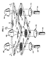
- FIG. 1 there are shown schematically first and second photomasks 11 and 12 for illustrating the general principles of the invention.
- the pattern of the photomasks nor the wafer between them which is to be exposed has been shown.
- the only devices shown are those for aiding in mask alignment.
- zone plates 13A, 13B, and 13C Arranged around a periphery of the lower photomask 11 are three zone plates 13A, 13B, and 13C. Aligned respectively with the zone plates on the upper photomask 12 are three transparent slits 14A, 14B, and 14C. As is known, zone plates are diffraction elements, which, when arranged in the shape of concentric circles, may act as circular lenses. Both the zone plates 13A-C and the transparent slits 14A-C may conveniently be made at the same time that the photolithographic mask patterns in the photomasks are made.
- Light from light sources 16A-C which may be optic fibers, is collimated by collimating lenses 17A-C and is directed through the zone plates 13A-C.
- the zone plates focus the light into beams which, when the masks are properly aligned, are transmitted through the corresponding transparent slits 14A-C.
- the masks are aligned by moving the upper photomask 12 in X,Y and ⁇ directions relative to the lower mask 11 until the three focused beams are transmitted through the three slits 14A-C.
- the upper photomask 12 is moved in a Y direction until focused light from zone plate 13A is transmitted through transparent slit 14A and detected by photodetector 18A.
- the photomask 12 may be slowly scanned in the Y direction to determine the position at which light transmitted through opening 14A is at a maximum.
- the position of maximum light power transmission indicates a precise centering of the transparent slit with respect to the light beam.
- the slits 14A-C have a long dimension transverse to the direction of scan during alignment.
- slit 14A used for Y direction alignment, has a long dimension in the X direction.
- Slits 14C and 14B are arranged along a line parallel to the Y axis.
- the upper photomask is scanned in the X direction until light is initially detected by detectors 18B and 18C.
- An angular adjustment is made so that light is detected simultaneously by both detectors, 18B and 18C during a scan.
- Such adjustments may be made after repetitive slow X-direction scans to obtain maximum light power detection simultaneously by the detectors 18B and 18C, which indicates both X-direction and ⁇ alignment.
- masks 11 and 12 are fixed for exposure of the wafer.
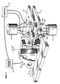
- FIG. 2 shows schematically a photomask alignment system in accordance with the invention that has been successfully used in the fabrication of optic fiber connectors. Elements having the same reference numbers as those of FIG. 1 perform the same functions and, for expediency, will not be further explained; however, it is the lower photomask that is actually moved into alignment, rather than the upper photomask as in FIG. 1.
- a photomask holder 20 supports photomask 11 and is driven by a stepper motor 21 in X and ⁇ directions as shown.
- Lenses 17B and 17C and optic fiber light sources 16B and 16C are fixed by an encapsulation to photomask 11 and are driven with it.
- Photomasks 11 and 12 are arranged on opposite sides of a silicon wafer (not shown) to be processed. The wafer is coated with a photoresist on top and bottom surfaces and both photomasks contain patterns to be transferred to the silicon wafer. After alignment, ultraviolet sources 24 and 25 expose the photoresist through the photomasks to define the patterns that are subsequently used to control etching of the silicon wafer. After masking and etching, the wafer is cut into chips that are thereafter used as optic fiber connectors.
- holder 20 The construction of holder 20 and the particular etching requirements for the wafer are such that the highly critical alignment capabilities of the invention are not required for alignment in the Y direction.
- the apparatus is intended for the fabrication of optical fiber connectors which require grooves on opposite sides of a chip that are extremely accurately aligned in the X and ⁇ directions for accurate intermeshing with the other elements. Notice that for ⁇ alignment, the holder 20 is rotated about an axis that is removed from photomasks 11 and 12.
- the photomasks are essentially glass plates.
- the mask pattern and the transparent slits are formed on the lower surface of photomask 12, while the zone plates and lower photomask pattern are formed on the upper surface of photomask 11.
- Slit 14B and zone plate 13B are shown in FIG. 3.
- the transparent slits and the zone plates can conveniently be made by photolithographic masking and etching simultaneously with the formation of the mask patterns on photomasks 11 and 12 and by the same process.
- the light sources 16B and 16C are optic fibers for transmitting light from a remote source and lenses 17B and 17C are glass lenses for collimating light from the optic fibers.
- the outputs of light detectors 18B and 18C are directed to a computer 27 which controls the stepper motor 21.
- the computer is programmed, using known techniques, to align the masks automatically in accordance with the invention.
- the computer could be programmed to detect maximum light intensity through the slit, as has been described above, a more sophisticated method has been found for more accurately centering the slit on th focused beam.
- the light beam focused on the slit, or on the upper photomask 12 prior to alignment has an intensity distribution as shown by curve 29 of FIG. 4.
- Curve 29, the light distribution resulting from zone plate focusing, is known in the art as an Airy function.
- the spot size is taken as the distance d between curve segments at one-half the maximum intensity.
- the resultant light power, or integrated light intensity, detected by the photodetector varies with distance, as shown by curve 30 of FIG. 5.
- Curve 30 is known mathematically as a convolution of the curve 29 of FIG. 4 and of the rectangular slit.
- Point 31 represents the distance along the scan at which light begins to enter the slit and point 32 is the point at which the light beam leaves the slit. Since the spot has a finite width, the distance between 31 and 32 is somewhat greater than the actual width of the slit.
- Detection of the precise maximum may be somewhat difficult because the rate of change of slope of the curve at its maximum is relatively small. Instead, after the slit has initially been detected, a slow stepped scan is made such that three equally spaced samples of light output are taken as the beam traverses the slit. The computer fits these samples to a parabolic function to determine the location of the central peak. The initiation of a subsequent scan is adjusted to make the function more centered, and the operation is iterated until centering is achieved.
- the scan steps were each 2.5 microns.
- the slit width was 0.5 microns.
- each step was 1.5 microns, which was appropriate for giving three readings within the slit width.
- the one-half maximum spot size was 2.5 microns; however, the detectable spot size width was significantly larger.
- the angular or ⁇ alignment is done in conjunction with the X-direction alignment.
- the extent to which light is not detected simultaneously by the two detectors, and the order in which light is detected, indicates the magnitude and direction of angular misalignment.
- the computer is programmed to make a ⁇ adjustment during both the fast scans and the slow scans. After each show scan, both the initial location of the successive scan and the angular location of the mask are adjusted and scanning is repeated until accurate centering of both beams on both slits is simultaneously obtained.
- the masks are fixed on opposite sides of the wafer and exposures of both sides of the wafer by sources 24 and 25 are made.
Landscapes
- Physics & Mathematics (AREA)
- General Physics & Mathematics (AREA)
- Engineering & Computer Science (AREA)
- Multimedia (AREA)
- Exposure And Positioning Against Photoresist Photosensitive Materials (AREA)
- Exposure Of Semiconductors, Excluding Electron Or Ion Beam Exposure (AREA)
- Investigating Or Analysing Materials By Optical Means (AREA)
Abstract
Description
- This invention relates to mask aligning methods, and, more particularly, to methods for aligning photolithographic masks (photomasks) on opposite sides of a flat workpiece.
- Photolithographic masking and etching is widely understood because of its extensive use in the fabrication of integrated circuits. In such processes, a semiconductor wafer is coated with a thin layer of photoresist material and is exposed to actinic light though a patterned photomask. After development, the photoresist coating itself acts as a mask to permit selective processing, such as selective etching, of the wafer.
- It has been found that the same process is useful for making optic fiber connectors from silicon wafers. Each connector comprises a silicon chip having grooves on opposite sides which are used to contain optic fibers and to align the connector. Since the alignment of optic fibers for lightwave transmission is extremely critical, it is important that the support grooves be accurately located to within tolerances that are typically less than one micron. For this reason, in the fabrication of such connectors, it is critical to align accurately photomasks on opposite sides of a semiconductor wafer that has been coated with photoresist material.
- The U.S. Patent of K.H. Chou, 3,963,489, issued June 15, 1976, is an example of prior art teachings of methods for aligning photomasks on opposite sides of a semiconductor wafer. The Chou technique uses indexing indicia on corresponding portions of the two photomasks that overlap the wafer contained between them. By properly aligning these indicia, one aligns the mask patterns of the two masks with respect to the intervening semiconductor wafer.
- A problem with using a scheme such as this for aligning masks with submicron tolerances is that a sufficiently high-power microscope for making the alignment will normally have a smaller depth of field than the separation of the two masks. Thus, the operator cannot see both alignment indicia simultaneously during the alignment operation. One way of meeting this problem would be to align the two masks while they are in close contact and then separate them to incorporate the wafer. In practice, it has been found to be extremely difficult, if not impossible, to make the required mechanical separation while maintaining the required close tolerances.
- In accordance with the invention, these problems are solved by making a plurality of zone plates on the periphery of one of the masks and a plurality of transparent slits on the periphery of the other mask, each slit being aligned with a corresponding zone plate. The masks are then conveniently aligned on opposite sides of a wafer by directing collimated light through one of the zone plates and then moving the masks relative to each other until the light beam focused by the zone plate is transmitted through a corresponding transparent slit. Three zone plates with corresponding transparent slits may be used for aligning the mask in X,Y and angular (or ϑ) directions.
- Transmission of the light beam through a transparent slit is conveniently detected automatically by a light detector. As will be explained in more detail below, a high degree of alignment accuracy can be obtained by scanning the light beam across the transparent slit, making three light intensity measurements during the scan and using a computer to fit the three intensity points to a parabolic curve. The computer can then determine the maximum of the parabolic curve, which will then correspond to the center of the transparent slit and move the mask relative to the light beam to get precise centering of the light beam on the slit.
- These and other objects and features of the invention will be better understood from a consideration of the following detailed description taken in conjunction with the accompanying drawing.
-
- FIG. 1 is a schematic illustration of apparatus for aligning photomasks in accordance with one embodiment of the invention;
- FIG. 2 is a schematic illustration of mask alignment and exposure apparatus in accordance with another embodiment of the invention;
- FIG. 3 is an expanded view of a portion of the apparatus of FIG. 2.
- FIG. 4 is a graph of light intensity vs. distance generated by the light beam shown in FIG. 3; and
- FIG. 5 is a graph of light power vs. distance as generated by the apparatus of FIGS. 2 and 3.
- Referring now to FIG. 1, there are shown schematically first and
second photomasks - Arranged around a periphery of the
lower photomask 11 are threezone plates upper photomask 12 are threetransparent slits zone plates 13A-C and thetransparent slits 14A-C may conveniently be made at the same time that the photolithographic mask patterns in the photomasks are made. - Light from
light sources 16A-C, which may be optic fibers, is collimated by collimatinglenses 17A-C and is directed through thezone plates 13A-C. The zone plates focus the light into beams which, when the masks are properly aligned, are transmitted through the correspondingtransparent slits 14A-C. - In accordance with the invention, the masks are aligned by moving the
upper photomask 12 in X,Y and ϑ directions relative to thelower mask 11 until the three focused beams are transmitted through the threeslits 14A-C. Preferably, theupper photomask 12 is moved in a Y direction until focused light fromzone plate 13A is transmitted throughtransparent slit 14A and detected byphotodetector 18A. After initial detection, thephotomask 12 may be slowly scanned in the Y direction to determine the position at which light transmitted through opening 14A is at a maximum. The position of maximum light power transmission of course indicates a precise centering of the transparent slit with respect to the light beam. Theslits 14A-C have a long dimension transverse to the direction of scan during alignment. For example,slit 14A, used for Y direction alignment, has a long dimension in the X direction.Slits - After Y direction alignment, the upper photomask is scanned in the X direction until light is initially detected by
detectors detectors thru detectors 18A-C,masks - FIG. 2 shows schematically a photomask alignment system in accordance with the invention that has been successfully used in the fabrication of optic fiber connectors. Elements having the same reference numbers as those of FIG. 1 perform the same functions and, for expediency, will not be further explained; however, it is the lower photomask that is actually moved into alignment, rather than the upper photomask as in FIG. 1.
- A
photomask holder 20 supportsphotomask 11 and is driven by astepper motor 21 in X and ϑ directions as shown.Lenses fiber light sources Photomasks ultraviolet sources - The construction of
holder 20 and the particular etching requirements for the wafer are such that the highly critical alignment capabilities of the invention are not required for alignment in the Y direction. Specifically, the apparatus is intended for the fabrication of optical fiber connectors which require grooves on opposite sides of a chip that are extremely accurately aligned in the X and ϑ directions for accurate intermeshing with the other elements. Notice that for ϑ alignment, theholder 20 is rotated about an axis that is removed fromphotomasks - The photomasks, portions of which are shown in greater detail in FIG. 2, are essentially glass plates. The mask pattern and the transparent slits are formed on the lower surface of
photomask 12, while the zone plates and lower photomask pattern are formed on the upper surface ofphotomask 11.Slit 14B andzone plate 13B are shown in FIG. 3. The transparent slits and the zone plates can conveniently be made by photolithographic masking and etching simultaneously with the formation of the mask patterns onphotomasks - The
light sources lenses light detectors computer 27 which controls thestepper motor 21. The computer is programmed, using known techniques, to align the masks automatically in accordance with the invention. - While the computer could be programmed to detect maximum light intensity through the slit, as has been described above, a more sophisticated method has been found for more accurately centering the slit on th focused beam. The light beam focused on the slit, or on the
upper photomask 12 prior to alignment, has an intensity distribution as shown bycurve 29 of FIG. 4.Curve 29, the light distribution resulting from zone plate focusing, is known in the art as an Airy function. The spot size is taken as the distance d between curve segments at one-half the maximum intensity. As the spot illustrated in FIG. 4 is scanned across the rectangular slit, the resultant light power, or integrated light intensity, detected by the photodetector varies with distance, as shown bycurve 30 of FIG. 5.Curve 30 is known mathematically as a convolution of thecurve 29 of FIG. 4 and of the rectangular slit.Point 31 represents the distance along the scan at which light begins to enter the slit andpoint 32 is the point at which the light beam leaves the slit. Since the spot has a finite width, the distance between 31 and 32 is somewhat greater than the actual width of the slit. - Detection of the precise maximum, as mentioned before, may be somewhat difficult because the rate of change of slope of the curve at its maximum is relatively small. Instead, after the slit has initially been detected, a slow stepped scan is made such that three equally spaced samples of light output are taken as the beam traverses the slit. The computer fits these samples to a parabolic function to determine the location of the central peak. The initiation of a subsequent scan is adjusted to make the function more centered, and the operation is iterated until centering is achieved.
- With three samples, centering occurs when the two outer samples are equal. For example, assume that the set of samples taken during the first slow scan were
points point 34 is lower thanpoint 36, the successive scan must be initiated at a location displaced slightly to the right. This will movepoint 34 "up the curve" andpoint 36 "down the curve". When the light power at points 34 and 36 is equal, then point 35 can be taken as being at the center of the slit and precise alignment is obtained. Such alignment is automatic and is made to tolerances of less than one micron. - During the rapid first scan for making the initial light detection, the scan steps were each 2.5 microns. The slit width was 0.5 microns. During the slow scan, each step was 1.5 microns, which was appropriate for giving three readings within the slit width. The one-half maximum spot size was 2.5 microns; however, the detectable spot size width was significantly larger.
- The angular or ϑ alignment is done in conjunction with the X-direction alignment. The extent to which light is not detected simultaneously by the two detectors, and the order in which light is detected, indicates the magnitude and direction of angular misalignment. The computer is programmed to make a ϑ adjustment during both the fast scans and the slow scans. After each show scan, both the initial location of the successive scan and the angular location of the mask are adjusted and scanning is repeated until accurate centering of both beams on both slits is simultaneously obtained. After alignment, the masks are fixed on opposite sides of the wafer and exposures of both sides of the wafer by
sources - The specific embodiments described are intended to be merely illustrative of the invention. Other radiative forms may be the functional equivalents of light beams. Relative movement of the beam with respect to the transparent slit implies that either the beam or the slit may be stationary. Various other modifications and embodiments may be made by those skilled in the art without departing from the spirit and scope of the invention.
Claims (17)
forming at least a first zone plate in the first mask;
forming at least a first transparent slit in the second mask at a predetermined location with respect to the location in the first mask of the first zone plate; and
wherein the alignment step comprises the step of directing a light beam through the first zone plate toward the second mask and moving the second mask relative to the first mask until the light beam is transmitted through the first transparent slit.
forming a second zone plate in the first mask;
forming a second transparent slit in the second mask; and
wherein the alignment step further comprises the steps of directing a light beam through the second zone plate toward the second mask and moving the second mask relative to the first mask until the second light beam is transmitted through the second transparent slit.
after the light beam is first transmitted through the first transparent slit, the second mask is moved relative to the first mask such as to cause the light beam to scan the width of the first transparent slit;
during such scan a plurality of measurements of light intensity through the slit is made;
the measurements are fitted to a parabola; and
thereafter the parabola is used to locate the second mask such that the center of the first transparent slit substantially coincides with the center of the light beam.
the light beam is caused to scan the width of the first transparent slit repetitively;
during each scan, three measurements of light intensity through the slit are made;
after each scan, the location of the initiation of successive scans is changed until two of the three measurements are substantially equal and the three measurements of light intensity vs. distance substantially describe a parabola; and
such parabola is used to center the first transparent slit on the light beam.
the step of moving the second mask relative to the first mask comprises the step of fixing the second mask with respect to a reference structure and moving the first mask relative to the reference structure, and wherein the light beam is fixed with respect to the first mask.
forming a first opening in the first mask;
forming a second opening in the second mask in alignment with the first opening; and
wherein the alignment step comprises the steps of directing a light beam through the first opening toward the second mask and causing relative movement of the first mask with respect to the second mask until the light beam is transmitted through both the first and the second openings.
the first opening is a zone plate;
the second opening is transparent slit; and
a photodetector is used to detect simultaneous transmission of the light beam through the first and second openings.
the step of causing relative movement of the first mask with respect to the second mask comprises the step of repeatedly scanning the opening with the light beam to determine the location at which light transmission through the first and second openings is at a maximum, and fixing the second mask with respect to the first mask at such location that light transmission through the first and second openings is at a maximum.
forming a third opening in the first mask;
forming a fourth opening in second mask in alignment with the third opening; and
wherein the alignment step comprises the steps of directing a second light beam through the third opening toward the second mask and causing movement of the first mask relative to the second mask until the second light beam is transmitted through both the third and fourth openings.
Applications Claiming Priority (2)
| Application Number | Priority Date | Filing Date | Title |
|---|---|---|---|
| US07/069,901 US4835078A (en) | 1987-07-06 | 1987-07-06 | Method for aligning photomasks |
| US69901 | 1987-07-06 |
Publications (3)
| Publication Number | Publication Date |
|---|---|
| EP0298642A2 true EP0298642A2 (en) | 1989-01-11 |
| EP0298642A3 EP0298642A3 (en) | 1989-04-26 |
| EP0298642B1 EP0298642B1 (en) | 1992-08-26 |
Family
ID=22091910
Family Applications (1)
| Application Number | Title | Priority Date | Filing Date |
|---|---|---|---|
| EP88305879A Expired - Lifetime EP0298642B1 (en) | 1987-07-06 | 1988-06-28 | Method for aligning photomasks |
Country Status (9)
| Country | Link |
|---|---|
| US (1) | US4835078A (en) |
| EP (1) | EP0298642B1 (en) |
| JP (1) | JPH0766904B2 (en) |
| KR (1) | KR970004887B1 (en) |
| CA (1) | CA1296180C (en) |
| DE (1) | DE3874028T2 (en) |
| DK (1) | DK373188A (en) |
| ES (1) | ES2034237T3 (en) |
| SG (1) | SG61093G (en) |
Cited By (5)
| Publication number | Priority date | Publication date | Assignee | Title |
|---|---|---|---|---|
| EP0752600A3 (en) * | 1995-07-06 | 1997-08-27 | Dainippon Printing Co Ltd | Hologram color filter, and its fabrication method |
| WO1998040792A1 (en) * | 1997-03-10 | 1998-09-17 | Ohlig Albert H | System and method for optically aligning films and substrates used in printed circuit boards |
| CN101452228B (en) * | 2007-11-29 | 2010-11-17 | 富葵精密组件(深圳)有限公司 | Automatic alignment device |
| CN102608877A (en) * | 2012-03-30 | 2012-07-25 | 上海华力微电子有限公司 | Photoetching nesting method and photoetching method |
| CN116430579A (en) * | 2022-12-21 | 2023-07-14 | 西安应用光学研究所 | A Photoelectric Aiming Method Based on Oscillating Slit |
Families Citing this family (24)
| Publication number | Priority date | Publication date | Assignee | Title |
|---|---|---|---|---|
| US5325176A (en) * | 1988-02-16 | 1994-06-28 | Canon Kabushiki Kaisha | Position detecting method and apparatus including Fraunhofer diffraction detector |
| US5319444A (en) * | 1988-02-16 | 1994-06-07 | Canon Kabushiki Kaisha | Position detecting method and apparatus |
| US5262257A (en) * | 1989-07-13 | 1993-11-16 | Canon Kabushiki Kaisha | Mask for lithography |
| US5288729A (en) * | 1989-10-07 | 1994-02-22 | Kabushiki Kaisha Toshiba | Exposing method and apparatus |
| US5135590A (en) * | 1991-05-24 | 1992-08-04 | At&T Bell Laboratories | Optical fiber alignment method |
| US5170058A (en) * | 1991-10-30 | 1992-12-08 | International Business Machines Corporation | Apparatus and a method for alignment verification having an opaque work piece between two artwork masters |
| JPH05216209A (en) * | 1992-02-03 | 1993-08-27 | Nikon Corp | Photo mask |
| US5504596A (en) * | 1992-12-21 | 1996-04-02 | Nikon Corporation | Exposure method and apparatus using holographic techniques |
| FR2704660B1 (en) * | 1993-04-27 | 1995-07-13 | Sgs Thomson Microelectronics | Masks for a double-sided exposure machine. |
| US5346583A (en) * | 1993-09-02 | 1994-09-13 | At&T Bell Laboratories | Optical fiber alignment techniques |
| JPH0961111A (en) * | 1995-08-28 | 1997-03-07 | Nikon Corp | Pattern coordinate measuring method and device |
| KR0172790B1 (en) * | 1995-09-18 | 1999-03-20 | 김영환 | Phase inversion mask and manufacturing method thereof |
| JPH09166416A (en) * | 1995-12-13 | 1997-06-24 | Mitsubishi Electric Corp | Reticle pattern relative displacement amount measuring method and reticle pattern relative displacement amount measuring device |
| US5627378A (en) * | 1996-02-28 | 1997-05-06 | Orc Electronic Products, A Divison Of Benson Eyecare Corporation | Die set for automatic UV exposure system |
| US6324010B1 (en) | 1999-07-19 | 2001-11-27 | Eastman Kodak Company | Optical assembly and a method for manufacturing lens systems |
| US7086134B2 (en) * | 2000-08-07 | 2006-08-08 | Shipley Company, L.L.C. | Alignment apparatus and method for aligning stacked devices |
| US6737223B2 (en) * | 2000-08-07 | 2004-05-18 | Shipley Company, L.L.C. | Fiber optic chip with lenslet array and method of fabrication |
| US6587618B2 (en) * | 2001-03-16 | 2003-07-01 | Corning Incorporated | Collimator array and method and system for aligning optical fibers to a lens array |
| US6621553B2 (en) | 2001-03-30 | 2003-09-16 | Perkinelmer, Inc. | Apparatus and method for exposing substrates |
| JP2004253741A (en) * | 2003-02-21 | 2004-09-09 | Sumitomo Eaton Noba Kk | Transfer device and semiconductor manufacturing device |
| TWI506313B (en) * | 2011-12-27 | 2015-11-01 | Hon Hai Prec Ind Co Ltd | Optical fiber connector device |
| CN102759865B (en) * | 2012-07-26 | 2016-02-03 | 四川聚能核技术工程有限公司 | exposure alignment system |
| GB2563435A (en) * | 2017-06-16 | 2018-12-19 | The Univ Court Of The Univ Of St Andrews | Three-photon light sheet imaging |
| KR102721980B1 (en) | 2022-02-24 | 2024-10-25 | 삼성전자주식회사 | Substrate alignment apparatus and alightment metohd usging the same |
Family Cites Families (9)
| Publication number | Priority date | Publication date | Assignee | Title |
|---|---|---|---|---|
| US3264105A (en) * | 1962-05-31 | 1966-08-02 | Western Electric Co | Method of using a master art drawing to produce a two-sided printed circuit board |
| US3759767A (en) * | 1971-10-08 | 1973-09-18 | Western Electric Co | Mask alignment methods |
| US3963489A (en) * | 1975-04-30 | 1976-06-15 | Western Electric Company, Inc. | Method of precisely aligning pattern-defining masks |
| US4109158A (en) * | 1976-05-27 | 1978-08-22 | Western Electric Company, Inc. | Apparatus for positioning a pair of elements into aligned intimate contact |
| JPS5533146A (en) * | 1978-08-30 | 1980-03-08 | Dainippon Screen Mfg Co Ltd | Photoelectric element for detecting and positioning register mark for engraving |
| FR2436967A1 (en) * | 1978-09-19 | 1980-04-18 | Thomson Csf | METHOD FOR OPTICAL ALIGNMENT OF PATTERNS IN TWO CLOSE PLANS AND ALIGNMENT DEVICE IMPLEMENTING SUCH A METHOD |
| DE3121666A1 (en) * | 1981-05-30 | 1982-12-16 | Ibm Deutschland Gmbh, 7000 Stuttgart | METHOD AND DEVICE FOR THE MUTUAL ALIGNMENT OF OBJECTS IN X-RAY AND CARPULAR RAY EXPOSURE PROCESSES |
| US4545683A (en) * | 1983-02-28 | 1985-10-08 | The Perkin-Elmer Corporation | Wafer alignment device |
| DE3443178A1 (en) * | 1984-11-27 | 1986-05-28 | Hoechst Ag, 6230 Frankfurt | METHOD FOR POSITIONING PRINTING FORMS BEFORE PUNCHING REGISTER HOLES AND ARRANGEMENT FOR CARRYING OUT THE METHOD |
-
1987
- 1987-07-06 US US07/069,901 patent/US4835078A/en not_active Expired - Lifetime
-
1988
- 1988-06-28 EP EP88305879A patent/EP0298642B1/en not_active Expired - Lifetime
- 1988-06-28 ES ES198888305879T patent/ES2034237T3/en not_active Expired - Lifetime
- 1988-06-28 DE DE8888305879T patent/DE3874028T2/en not_active Expired - Fee Related
- 1988-06-30 CA CA000570949A patent/CA1296180C/en not_active Expired - Lifetime
- 1988-07-02 KR KR1019880008209A patent/KR970004887B1/en not_active Expired - Fee Related
- 1988-07-05 DK DK373188A patent/DK373188A/en unknown
- 1988-07-06 JP JP63167035A patent/JPH0766904B2/en not_active Expired - Lifetime
-
1993
- 1993-05-07 SG SG610/93A patent/SG61093G/en unknown
Cited By (10)
| Publication number | Priority date | Publication date | Assignee | Title |
|---|---|---|---|---|
| EP0752600A3 (en) * | 1995-07-06 | 1997-08-27 | Dainippon Printing Co Ltd | Hologram color filter, and its fabrication method |
| US6426812B2 (en) | 1995-07-06 | 2002-07-30 | Dai Nippon Printing Co., Ltd. | Hologram color filter, and its fabrication method |
| EP1367415A3 (en) * | 1995-07-06 | 2004-08-18 | Dai Nippon Printing Co., Ltd. | Hologram color filter, and its fabrication method |
| WO1998040792A1 (en) * | 1997-03-10 | 1998-09-17 | Ohlig Albert H | System and method for optically aligning films and substrates used in printed circuit boards |
| GB2340960A (en) * | 1997-03-10 | 2000-03-01 | Albert H Ohlig | System and method for optically aligning films and substrates used in printed circuit boards |
| US6156220A (en) * | 1997-03-10 | 2000-12-05 | Ohlig; Albert H. | System and method for optically aligning films and substrates used in printed circuit boards |
| US6193899B1 (en) | 1997-03-10 | 2001-02-27 | Albert H. Ohlig | System and method for optically aligning films and substrates used in printed circuit boards |
| CN101452228B (en) * | 2007-11-29 | 2010-11-17 | 富葵精密组件(深圳)有限公司 | Automatic alignment device |
| CN102608877A (en) * | 2012-03-30 | 2012-07-25 | 上海华力微电子有限公司 | Photoetching nesting method and photoetching method |
| CN116430579A (en) * | 2022-12-21 | 2023-07-14 | 西安应用光学研究所 | A Photoelectric Aiming Method Based on Oscillating Slit |
Also Published As
| Publication number | Publication date |
|---|---|
| ES2034237T3 (en) | 1993-04-01 |
| KR970004887B1 (en) | 1997-04-08 |
| EP0298642A3 (en) | 1989-04-26 |
| SG61093G (en) | 1993-07-09 |
| EP0298642B1 (en) | 1992-08-26 |
| CA1296180C (en) | 1992-02-25 |
| DE3874028D1 (en) | 1992-10-01 |
| US4835078A (en) | 1989-05-30 |
| DE3874028T2 (en) | 1993-01-07 |
| JPH0766904B2 (en) | 1995-07-19 |
| DK373188A (en) | 1989-01-07 |
| JPS6424420A (en) | 1989-01-26 |
| KR890002971A (en) | 1989-04-12 |
| DK373188D0 (en) | 1988-07-05 |
Similar Documents
| Publication | Publication Date | Title |
|---|---|---|
| EP0298642B1 (en) | Method for aligning photomasks | |
| US4441250A (en) | Apparatus for registering a mask pattern in a photo-etching apparatus for semiconductor devices | |
| USRE37391E1 (en) | Exposure method and projection exposure apparatus | |
| US4211489A (en) | Photomask alignment system | |
| US3783520A (en) | High accuracy alignment procedure utilizing moire patterns | |
| US4153371A (en) | Method and apparatus for reduction-projection type mask alignment | |
| US4037969A (en) | Zone plate alignment marks | |
| JP3181050B2 (en) | Projection exposure method and apparatus | |
| US3690881A (en) | Moire pattern aligning of photolithographic mask | |
| US4904087A (en) | Method for aligning photomasks | |
| KR930000878B1 (en) | Alignment System and Method of Mask and Semiconductor Wafer Using Linear Fresnel Zone Plate | |
| US4657379A (en) | Photomask and exposure apparatus using the same | |
| EP0031680B1 (en) | Focusing apparatus | |
| EP0341848B1 (en) | Optical alignment system for use in photolithography and having reduced reflectance errors | |
| US4422763A (en) | Automatic photomask alignment system for projection printing | |
| US4702606A (en) | Position detecting system | |
| US20140204355A1 (en) | Method for Exposing an Area on a Substrate to a Beam and Photolithographic System | |
| KR20010091971A (en) | Alignment apparatus, alignment method, exposure apparatus, and exposure method | |
| GB2133536A (en) | Sensing alignment | |
| GB2040444A (en) | Automatic Photomask Alignment System for Projection Printing | |
| US4292576A (en) | Mask-slice alignment method | |
| US5929529A (en) | Reticle semiconductor wafer, and semiconductor chip | |
| JP3368017B2 (en) | Position detecting device and method of manufacturing semiconductor device using the same | |
| US5247329A (en) | Projection type exposure method and apparatus | |
| USH1463H (en) | Method for detecting positions of photomask and substrate |
Legal Events
| Date | Code | Title | Description |
|---|---|---|---|
| PUAI | Public reference made under article 153(3) epc to a published international application that has entered the european phase |
Free format text: ORIGINAL CODE: 0009012 |
|
| AK | Designated contracting states |
Kind code of ref document: A2 Designated state(s): DE ES FR GB NL SE |
|
| PUAL | Search report despatched |
Free format text: ORIGINAL CODE: 0009013 |
|
| AK | Designated contracting states |
Kind code of ref document: A3 Designated state(s): DE ES FR GB NL SE |
|
| 17P | Request for examination filed |
Effective date: 19891018 |
|
| 17Q | First examination report despatched |
Effective date: 19910621 |
|
| GRAA | (expected) grant |
Free format text: ORIGINAL CODE: 0009210 |
|
| AK | Designated contracting states |
Kind code of ref document: B1 Designated state(s): DE ES FR GB NL SE |
|
| REF | Corresponds to: |
Ref document number: 3874028 Country of ref document: DE Date of ref document: 19921001 |
|
| ET | Fr: translation filed | ||
| REG | Reference to a national code |
Ref country code: ES Ref legal event code: FG2A Ref document number: 2034237 Country of ref document: ES Kind code of ref document: T3 |
|
| PLBE | No opposition filed within time limit |
Free format text: ORIGINAL CODE: 0009261 |
|
| STAA | Information on the status of an ep patent application or granted ep patent |
Free format text: STATUS: NO OPPOSITION FILED WITHIN TIME LIMIT |
|
| 26N | No opposition filed | ||
| EAL | Se: european patent in force in sweden |
Ref document number: 88305879.4 |
|
| PGFP | Annual fee paid to national office [announced via postgrant information from national office to epo] |
Ref country code: SE Payment date: 19990322 Year of fee payment: 12 |
|
| PGFP | Annual fee paid to national office [announced via postgrant information from national office to epo] |
Ref country code: ES Payment date: 19990607 Year of fee payment: 12 |
|
| PG25 | Lapsed in a contracting state [announced via postgrant information from national office to epo] |
Ref country code: SE Free format text: LAPSE BECAUSE OF NON-PAYMENT OF DUE FEES Effective date: 20000629 Ref country code: ES Free format text: LAPSE BECAUSE OF NON-PAYMENT OF DUE FEES Effective date: 20000629 |
|
| EUG | Se: european patent has lapsed |
Ref document number: 88305879.4 |
|
| PGFP | Annual fee paid to national office [announced via postgrant information from national office to epo] |
Ref country code: GB Payment date: 20010525 Year of fee payment: 14 Ref country code: FR Payment date: 20010525 Year of fee payment: 14 |
|
| PGFP | Annual fee paid to national office [announced via postgrant information from national office to epo] |
Ref country code: NL Payment date: 20010529 Year of fee payment: 14 |
|
| PGFP | Annual fee paid to national office [announced via postgrant information from national office to epo] |
Ref country code: DE Payment date: 20010629 Year of fee payment: 14 |
|
| REG | Reference to a national code |
Ref country code: GB Ref legal event code: IF02 |
|
| PG25 | Lapsed in a contracting state [announced via postgrant information from national office to epo] |
Ref country code: GB Free format text: LAPSE BECAUSE OF NON-PAYMENT OF DUE FEES Effective date: 20020628 |
|
| PG25 | Lapsed in a contracting state [announced via postgrant information from national office to epo] |
Ref country code: NL Free format text: LAPSE BECAUSE OF NON-PAYMENT OF DUE FEES Effective date: 20030101 Ref country code: DE Free format text: LAPSE BECAUSE OF NON-PAYMENT OF DUE FEES Effective date: 20030101 |
|
| GBPC | Gb: european patent ceased through non-payment of renewal fee |
Effective date: 20020628 |
|
| PG25 | Lapsed in a contracting state [announced via postgrant information from national office to epo] |
Ref country code: FR Free format text: LAPSE BECAUSE OF NON-PAYMENT OF DUE FEES Effective date: 20030228 |
|
| NLV4 | Nl: lapsed or anulled due to non-payment of the annual fee |
Effective date: 20030101 |
|
| REG | Reference to a national code |
Ref country code: ES Ref legal event code: FD2A Effective date: 20030203 |
|
| REG | Reference to a national code |
Ref country code: FR Ref legal event code: ST |