EP0289948B1 - A polarization controller - Google Patents
A polarization controller Download PDFInfo
- Publication number
- EP0289948B1 EP0289948B1 EP88106897A EP88106897A EP0289948B1 EP 0289948 B1 EP0289948 B1 EP 0289948B1 EP 88106897 A EP88106897 A EP 88106897A EP 88106897 A EP88106897 A EP 88106897A EP 0289948 B1 EP0289948 B1 EP 0289948B1
- Authority
- EP
- European Patent Office
- Prior art keywords
- waveguide
- polarisation
- light
- electrodes
- arbitrary
- Prior art date
- Legal status (The legal status is an assumption and is not a legal conclusion. Google has not performed a legal analysis and makes no representation as to the accuracy of the status listed.)
- Expired - Lifetime
Links
Images

Classifications
-
- G—PHYSICS
- G02—OPTICS
- G02F—OPTICAL DEVICES OR ARRANGEMENTS FOR THE CONTROL OF LIGHT BY MODIFICATION OF THE OPTICAL PROPERTIES OF THE MEDIA OF THE ELEMENTS INVOLVED THEREIN; NON-LINEAR OPTICS; FREQUENCY-CHANGING OF LIGHT; OPTICAL LOGIC ELEMENTS; OPTICAL ANALOGUE/DIGITAL CONVERTERS
- G02F1/00—Devices or arrangements for the control of the intensity, colour, phase, polarisation or direction of light arriving from an independent light source, e.g. switching, gating or modulating; Non-linear optics
- G02F1/01—Devices or arrangements for the control of the intensity, colour, phase, polarisation or direction of light arriving from an independent light source, e.g. switching, gating or modulating; Non-linear optics for the control of the intensity, phase, polarisation or colour
- G02F1/03—Devices or arrangements for the control of the intensity, colour, phase, polarisation or direction of light arriving from an independent light source, e.g. switching, gating or modulating; Non-linear optics for the control of the intensity, phase, polarisation or colour based on ceramics or electro-optical crystals, e.g. exhibiting Pockels effect or Kerr effect
- G02F1/035—Devices or arrangements for the control of the intensity, colour, phase, polarisation or direction of light arriving from an independent light source, e.g. switching, gating or modulating; Non-linear optics for the control of the intensity, phase, polarisation or colour based on ceramics or electro-optical crystals, e.g. exhibiting Pockels effect or Kerr effect in an optical waveguide structure
- G02F1/0353—Devices or arrangements for the control of the intensity, colour, phase, polarisation or direction of light arriving from an independent light source, e.g. switching, gating or modulating; Non-linear optics for the control of the intensity, phase, polarisation or colour based on ceramics or electro-optical crystals, e.g. exhibiting Pockels effect or Kerr effect in an optical waveguide structure involving an electro-optic TE-TM mode conversion
-
- G—PHYSICS
- G02—OPTICS
- G02F—OPTICAL DEVICES OR ARRANGEMENTS FOR THE CONTROL OF LIGHT BY MODIFICATION OF THE OPTICAL PROPERTIES OF THE MEDIA OF THE ELEMENTS INVOLVED THEREIN; NON-LINEAR OPTICS; FREQUENCY-CHANGING OF LIGHT; OPTICAL LOGIC ELEMENTS; OPTICAL ANALOGUE/DIGITAL CONVERTERS
- G02F1/00—Devices or arrangements for the control of the intensity, colour, phase, polarisation or direction of light arriving from an independent light source, e.g. switching, gating or modulating; Non-linear optics
- G02F1/01—Devices or arrangements for the control of the intensity, colour, phase, polarisation or direction of light arriving from an independent light source, e.g. switching, gating or modulating; Non-linear optics for the control of the intensity, phase, polarisation or colour
- G02F1/0136—Devices or arrangements for the control of the intensity, colour, phase, polarisation or direction of light arriving from an independent light source, e.g. switching, gating or modulating; Non-linear optics for the control of the intensity, phase, polarisation or colour for the control of polarisation, e.g. state of polarisation [SOP] control, polarisation scrambling, TE-TM mode conversion or separation
-
- G—PHYSICS
- G02—OPTICS
- G02F—OPTICAL DEVICES OR ARRANGEMENTS FOR THE CONTROL OF LIGHT BY MODIFICATION OF THE OPTICAL PROPERTIES OF THE MEDIA OF THE ELEMENTS INVOLVED THEREIN; NON-LINEAR OPTICS; FREQUENCY-CHANGING OF LIGHT; OPTICAL LOGIC ELEMENTS; OPTICAL ANALOGUE/DIGITAL CONVERTERS
- G02F2201/00—Constructional arrangements not provided for in groups G02F1/00 - G02F7/00
- G02F2201/06—Constructional arrangements not provided for in groups G02F1/00 - G02F7/00 integrated waveguide
- G02F2201/066—Constructional arrangements not provided for in groups G02F1/00 - G02F7/00 integrated waveguide channel; buried
Definitions
- the invention relates to a polarization controller, and more particularly to a waveguide type of a polarization controller which is applied to an optical communication system, an optical fiber sensor and so on.
- a polarization controller for converting an arbitrary polarization to a constant linear polarization or another arbitrary polarization is provided in an optical system such as an optical communication system, an optical fiber sensor and so on.
- a waveguide type of a polarization controller is advantageous in that the weight of the controller is light, the productivity thereof is high, integration with other devices is easy so that the polarization controller is expected to be widely put into a practical use.
- the conventional polarization controller is of a tandem structure which is composed of a phase shifter and a mode converter, and comprises an optical channel waveguide (simply called “a waveguide” hereinafter) extended along Z-axis on a LiNbO3 substrate, a first and second electrodes provided on both sides of the waveguide in a region of the phase shifter of the substrate, and a first to third electrodes provided on the waveguide and both sides thereof in a region of the mode converter.
- a waveguide optical channel waveguide
- the first electrode is connected to the ground, and an adjustable voltage V1 is applied to the second electrode.
- the first electrode is connected on the side of the waveguide to the ground, an adjustable voltage V2 is applied on the waveguide to the second electrode, and a constant voltage V3 is applied on the other side of the waveguide to the third electrode.
- the birefringence of the waveguide is compensated to result in an isotropic condition in accordance with the applied voltage V3, and an extent of a birefringence is changed in a direction orthogonal to the light propagation direction of the waveguide and in a direction of 45 degrees in regard to the surface of the substrate.
- the latter polarization controller comprises a further phase shifter which is the same structure as that of the phase shifter in the former polarization controller.
- the latter polarization controller comprises a first and second phase shifters and a mode converter which is positioned between the first and second phase shifters wherein the mode converter is also the same structure as that of the mode converter in the former polarization controller.
- the same adjustments of voltages are performed in the first and second phase shifters and the mode converter as in the former polarization controller described above so that an input light of an arbitrary polarization which is incident to the polarization controller is converted to an output light of another arbitrary polarization which is supplied therefrom to a next stage.
- the aforementioned voltage V1 must be kept increasing or decreasing to convert a phase difference of TE and TM modes of an input light, which is incident to the phase shifter, to ⁇ /2 successively in a case where the phase difference continues to be increased or decreased.
- it is not allowed to increase or decrease the voltage V1 which is applied to the second electrodes to an unlimited extent because withstand voltage of the second electrode is limited.
- EP-A-0 287 359 constitutes prior art pursuant to Article 54 (3) and (4) EPC and discloses an optical signal control device with an optical waveguide on a substrate having an electro-optical effect.
- a birefringence of the optical waveguide is produced on a plane orthogonal to the light propagation direction by each of a plurality of electrode groups on the waveguide.
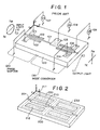
- Fig. 1 shows the conventional polarization controller which is composed of a phase shifter 120 and a mode converter 130.
- the phase shifter 120 comprises a waveguide 101 provided on a LiNbO3 substrate 100, a first electrode 102 provided on one side of the waveguide 101 and connected to the ground, and a second electrode 103 provided on the other side of the waveguide 101 and connected to a power source 107 from which an adjustable voltage V1 is applied thereto.
- the mode converter 130 comprises the waveguide 101 provided on the LiNbO3 substrate 100, a first electrode 104 provided on one side of the waveguide 101 and connected to the ground, a second electrode 105 provided on the waveguide 101 and connected to a power source 108 from which an adjustable voltage V2 is applied thereto, and a third electrode 106 provided on the other side of the waveguide 101 and connected to a power source 109 from which a constant voltage V3 is applied thereto.
- a polarization controller in the first embodiment according to the invention.
- the polarization controller comprises a waveguide 201 provided on a substrate 200 of LiNbO3 to extend in a direction of Z axis, and three electrodes 210, 211 and 212 of aluminum provided on the waveguide 201 and on both sides thereof whereby a first device 220 is formed on the substrate 200.
- the polarization controller further comprises a second device 230 which is connected in cascade with the first device 220 and is of the same structure as that of the first device 220.
- the waveguide 201 is formed by indiffusion of a 8 ⁇ m wide, 100 nm thick titanium stripe at 1025°C for 6 hours into the substrate 200, and is of a single mode excitation for both TE and TM modes. Lengths of the electrodes 210, 211 and 212 are 10 mm respectively, a width of the electrode 210 is 8 ⁇ m and widths of the electrodes 211 and 212 are 15 ⁇ m respectively. There are provided gaps of 4 ⁇ m on the substrate 200 respectively between the electrodes 210 and 211 and between the electrodes 210 and 212, and a SiO2 buffer layer (not shown) having a thickness of 300 nm by the CVD process between the waveguide 201 and the electrode 210. The buffer layer prevents light propagating through the waveguide 201 from being attenuated.
- the first device 220 In operation, when predetermined voltages which are described later are applied to the electrodes 210 and 211 in the first device 220, the first device 220 operates as a quarter-wave plate so that a retardation induced by electrooptic effect in the first device 220 is ⁇ /2, and a principal axis of a birefringence induced in the waveguide 201 is rotated in an arbitrary direction by adjusting the voltages applied to the electrodes 210 and 211. At the present stage, it is not required to keep increasing or decreasing the voltages which are applied to the electrodes 210 and 211 to rotate the principal axis because the voltages are changed periodically.
- the second device 230 is operated as a half-wave plate in which voltages applied to electrodes corresponding to the electrodes 210 and 211 to rotate a principal axis of a birefringence are changed periodically in the same manner as in the first device 220. For this reason, it is also not required to keep increasing or decreasing the voltages applied to the corresponding electrodes. Therefore, when the direction of the principal axis of birefringence induced in the waveguide 201 is adjusted in the first and second devices 220 and 230, an input light of an arbitrary polarization which is incident to the waveguide 201 of the first device 220 is converted to an output light of an arbitrary linear polarization to be supplied from the second device 230 to a next stage. In more detail, the input light of an arbitrary polarization is converted in the first device 220 to a light of a linear polarization which is then converted in the second device 230 to the output light of an arbitrary linear polarization.
- the polarization controller in the first embodiment there is no limitation in the operating range in which a polarization of an input light is controlled because none of the voltages applied to the electrodes 210 and 211 of the first device 220 and to the corresponding electrodes of the second device 230 does not exceed a specified voltage.
- the first and second devices 220 and 230 are monolithicly formed on the substrate 200, they may be fabricated separately and then connected in cascade with each other.
- a polarization controller as described in the first embodiment which operates as a waveplate wherein like parts are indicated by like reference numerals except that voltages V1 and V2 are applied from a power source 300 to electrodes 210 and 211, while electrode 212 is connected to the ground.
- voltages V1 and V2 are applied from a power source 300 to electrodes 210 and 211, while electrode 212 is connected to the ground.
- first device 220 of the polarization controller these may be also applied to the second device 230 thereof.
- electric fields Ex and Ey are produced in the waveguide 201 as illustrated therein.
- the electric field Ex is dominantly determined by the voltage V1
- Ey is dominantly determined by the voltage V2.
- the electric fields Ex and Ey are set to be predetermined levels by adjusting the voltages V1 and V2.
- the electric fields Ex and Ey are approximately defined in the equations (1).
- W1 is a gap between the electrodes 210 and 211 and between the electrodes 210 and 212
- W2 is a distance between the electrodes 211 and 212.
- a combined electric field E0 is defined in the following equations (2).
- ⁇ is an angle of the combined electric field E0 which is rotated in an anti-clock direction in regard to a reference line of the electric field Ey.
- the refractive index is changed in the waveguide 201 dependent on the combined electric field E0.
- the change of the refractive index is defined in the equations (3) in accordance with a refractive index ellipsoid which is formed on a X-Y plane orthogonal to the Z axis of the light propagating direction in the waveguide 201.
- n1 and n2 are dimensions of the major and minor axes of the ellipsoid
- n0 is the ordinary refractive index of the substrate 200
- ⁇ is an inclination angle of the minor and major axes
- r22 is a coefficient of an electrooptic effect of the substrate 200.
- the principal axis of a birefringence is rotated in a predetermined direction.
- a retardation is set to be ⁇ or ⁇ /2 by adjusting the electric field E0
- the first and second devices 220 and 230 are operated as a half-wave plate or a quarter-wave plate.
- the electric fields E0 which are required to provide a half-wave plate and a quarter-wave plate are defined in the equations (4) and (5) respectively.
- l is the length of the electrodes 210 and 211
- ⁇ is the wavelength of light which propagates through the waveguide 201.
- the voltages V1 and V2 applied to the electrodes 210 and 211 are obtained from the equations (1) and (2) as defined in the equation (6).
- the maximum values of the voltages V1 and V2 required for a half-wave plate operation are calculated to be 8.4 V and 33.6 V respectively.
- the voltages V1 and V2 which are required for a quarter-wave plate operation are half values of those which are required for a half-wave plate operation.
- anisotropy is induced in the waveguide 201 to a small extent due to the structural dispersion. For this reason, a predetermined level of a biased voltage is desired to be added to the voltage V2 to compensate the anisotropy.
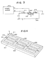
- a polarization controller in a second embodiment according to the invention.
- the polarization controller comprises a first, second and third devices 420, 430 and 440 provided in series on a substrate 400.
- the first device 420 comprises a waveguide 401, and electrodes 410, 411 and 412 provided on the waveguide 401 and on both sides thereof.
- the second and third devices 430 and 440 are of the same structure as that of the first device 420.
- the first and second devices 420 and 430 correspond to the first and second devices 220 and 230 of the polarization controller in the first embodiment, and the third device 440 operates as a quarter-wave plate.
- an input light of an arbitrary polarization which is incident on the first device 420 is converted therein to a light of a linear polarization which is then converted in the second device 430 to a light of an arbitrary linear polarization.
- the light of an arbitrary linear polarization is then converted in the third device 440 to a light of an arbitrary polarization which is supplied therefrom to a next stage as an output light.
- the heterodyne receiving circuit comprises the polarization controller 500 to which a signal light 510 is supplied, a local oscillator 501 for producing a local light, an optical coupler 502 for combining an output light supplied from the polarization controller 500 and the local light, an optical detector 503 for producing an intermediate frequency signal, a demodulator 504 for producing a data signal, a control unit 505 for producing a control signal in accordance with an intensity of the intermediate frequency signal, and a power source 506 for applying predetermined voltages Va1, Va2, Vb1 and Vb2 to the first and second devices of the polarization controller 500 in accordance with the control signal supplied from the control unit 505.
- the signal light 510 of an arbitrary polarization which is incident on the polarization controller 500 is converted therein to an output light of a horizontal linear polarization.
- the output light is combined in the optical coupler 502 with the local light of a horizontal linear polarization supplied from the local oscillator 501.
- the output light of the polarization controller 500 and the local light of the local oscillator 501 are of the same linear polarization so that the degradation of a receiver sensitivity is avoided by use of the polarization controller.
- the combined light of the optical coupler 502 is detected in the optical detector 503 to produce the intermediate frequency signal which is then demodulated in the demodulator 504.
- the demodulated signal is processed in following stages (not shown).
- an intensity of the intermediate frequency signal is monitored in the control unit 505 which produces a control signal dependent on the intensity thereby controlling the power source 506 to adjust the voltages Va1, Va2, Vb1 and Vb2 so that the intensity of the intermediate frequency signal is maximized.
- the maximum intensity of the intermediate frequency signal is obtained.
- the polarization controller 500 is composed of the first device for a quarter-wave plate to which the signal light 510 is supplied and the second device for a half-wave plate from which the output light is supplied to the optical coupler 502.
- the voltages Va1 and Va2 applied to the first device and those Vb1 and Vb2 applied to the second device are expressed in the equations (7) and (8) in accordance with the equations (6).
- Va0 and Vb0 are constant values determined by the definitions of the aforementioned "W1E0" and "W2E0".
- the directions of birefringence are rotated in predetermined directions in the first and second devices.
- the directions of the birefringence which are directly determined by the rotation angles ⁇ a and ⁇ b in the first and second devices are controlled to be appropriate directions so that the output light of a horizontal polarization is obtained.
- the rotation angles ⁇ a and ⁇ b are alternately controlled to be optimized by maximizing a horizontal polarization component of the output light so that the rotation angles ⁇ a and ⁇ b are gradually approaching the optimized angles by repeating the alternate controls. Even if the polarization of the signal light is fluctuated, the above described optimization of the rotation angles ⁇ a and ⁇ b is repeated so that a polarization control can be successively performed in the polarization controller 500.
- the polarization controller 500 may be positioned between the local oscillator 501 and the optical coupler 502 so that the polarization of the local light is converted to coincide with that of the signal light 510.
- the local light is incident on the second device for a half-wave plate, although the controlling procedure is the same as the above described one in which an intensity of the intermediate frequency signal is maximized.
- the waveguide is grown by the diffusion of Ti into the substrate of LiNbO3, this may be provided by the ion exchange process. Further, this may be of a ridge type or a rib type. Still further, the diffusion of MgO may be performed over the whole substrate after the diffusion of Ti into the substrate to provide the waveguide. This results in the decrease of a bias-voltage for compensating anisotropy in the waveguide because the waveguide becomes more isotropic.
- LiNbO3 is used for the substrate
- an electrooptic crystal with a three-fold axis an electrooptic ceramic such as PLZT etc. may be adopted for the substrate.
- the light propagating direction is along the optical axis.
Description
- The invention relates to a polarization controller, and more particularly to a waveguide type of a polarization controller which is applied to an optical communication system, an optical fiber sensor and so on.
- It is required that a polarization controller for converting an arbitrary polarization to a constant linear polarization or another arbitrary polarization is provided in an optical system such as an optical communication system, an optical fiber sensor and so on. Among polarization controllers, a waveguide type of a polarization controller is advantageous in that the weight of the controller is light, the productivity thereof is high, integration with other devices is easy so that the polarization controller is expected to be widely put into a practical use.
- A waveguide type of a conventional polarization controller has been described in a report entitled "Optical waveguide polarization controller in Z-propagation LiNbO₃" which was published as "NATIONAL CONFERENCE RECORD, 1986, OPTICAL AND RADIO WAVE ELECTRONICS, THE INSTITUTE OF ELECTRONICS AND COMMUNICATION ENGINEERS OF JAPAN". The conventional polarization controller is of a tandem structure which is composed of a phase shifter and a mode converter, and comprises an optical channel waveguide (simply called "a waveguide" hereinafter) extended along Z-axis on a LiNbO₃ substrate, a first and second electrodes provided on both sides of the waveguide in a region of the phase shifter of the substrate, and a first to third electrodes provided on the waveguide and both sides thereof in a region of the mode converter.
- In the phase shifter, the first electrode is connected to the ground, and an adjustable voltage V₁ is applied to the second electrode. In the mode converter, the first electrode is connected on the side of the waveguide to the ground, an adjustable voltage V₂ is applied on the waveguide to the second electrode, and a constant voltage V₃ is applied on the other side of the waveguide to the third electrode. As a result, an extent of a birefringence is changed in a direction orthogonal to the light propagation direction of the waveguide and parallel to the surface of the substrate in the region of the phase shifter. In the region of the mode converter, on the other hand, the birefringence of the waveguide is compensated to result in an isotropic condition in accordance with the applied voltage V₃, and an extent of a birefringence is changed in a direction orthogonal to the light propagation direction of the waveguide and in a direction of 45 degrees in regard to the surface of the substrate. If it is assumed that a phase difference between TE and TM modes is π/2 just in front of the mode converter by adjusting the voltage V₁ in the phase shifter, an input light of an arbitrary polarization which is incident to the polarization controller is converted to an output light of a linear polarization which is supplied therefrom to a next stage when an amplitude ratio of the TE and TM modes is controlled to be an appropriate ratio by adjusting the voltage V₂ in the mode converter.
- In addition to the polarization controller described above, another polarization controller has been proposed in US-A-4,691,984. The latter polarization controller comprises a further phase shifter which is the same structure as that of the phase shifter in the former polarization controller. In other words, the latter polarization controller comprises a first and second phase shifters and a mode converter which is positioned between the first and second phase shifters wherein the mode converter is also the same structure as that of the mode converter in the former polarization controller.
- In operation, the same adjustments of voltages are performed in the first and second phase shifters and the mode converter as in the former polarization controller described above so that an input light of an arbitrary polarization which is incident to the polarization controller is converted to an output light of another arbitrary polarization which is supplied therefrom to a next stage.
- According to the conventional polarization controller as formerly described, however, there is a disadvantage that the aforementioned voltage V₁ must be kept increasing or decreasing to convert a phase difference of TE and TM modes of an input light, which is incident to the phase shifter, to π/2 successively in a case where the phase difference continues to be increased or decreased. In this regard, it is not allowed to increase or decrease the voltage V₁ which is applied to the second electrodes to an unlimited extent because withstand voltage of the second electrode is limited. This results in the impossibility of controlling an arbitrary polarization in the phase shifter. That is, this means that there is a limitation of the operating range in controlling a fluctuation of a polarization in an input light which is incident on the phase shifter.
- Even in the polarization controller as proposed in US-A-4,691,984 the same disadvantage is observed.
- EP-A-0 287 359 constitutes prior art pursuant to Article 54 (3) and (4) EPC and discloses an optical signal control device with an optical waveguide on a substrate having an electro-optical effect. A birefringence of the optical waveguide is produced on a plane orthogonal to the light propagation direction by each of a plurality of electrode groups on the waveguide.
- Accordingly, it is an object of the invention to provide a polarization transformer in which there is no limitation in an operating range for the transformation of an input light polarization.
- It is a further object of the invention to provide a polarization transformer in which any fluctuation of an input light polarization can be controlled.
- This object is solved with the features of claim 1.
- The invention will be explained in more detail in conjunction with following drawings wherein,
- Fig. 1 is an explanatory view showing a conventional polarization controller,
- Fig. 2 is an explanatory view showing a polarization controller in a first embodiment according to the invention,
- Fig. 3 is a cross sectional view showing a device in the first embodiment which is operated as a waveplate.
- Fig. 4 is an explanatory view showing a polarization controller in a second embodiment according to the invention, and
- Fig. 5 is a block diagram showing an optical heterodyne receiving circuit in which a polarization controller in the first embodiment is utilized.
- Before explaining a polarization controller in a first embodiment according to the invention, the conventional polarization controller which has been described in the aforementioned report of "THE INSTITUTE OF ELECTRONICS AND COMMUNICATION ENGINEERS OF JAPAN" will be explained again. Fig. 1 shows the conventional polarization controller which is composed of a
phase shifter 120 and amode converter 130. Thephase shifter 120 comprises awaveguide 101 provided on aLiNbO₃ substrate 100, afirst electrode 102 provided on one side of thewaveguide 101 and connected to the ground, and asecond electrode 103 provided on the other side of thewaveguide 101 and connected to apower source 107 from which an adjustable voltage V₁ is applied thereto. Themode converter 130 comprises thewaveguide 101 provided on theLiNbO₃ substrate 100, afirst electrode 104 provided on one side of thewaveguide 101 and connected to the ground, asecond electrode 105 provided on thewaveguide 101 and connected to a power source 108 from which an adjustable voltage V₂ is applied thereto, and athird electrode 106 provided on the other side of thewaveguide 101 and connected to apower source 109 from which a constant voltage V₃ is applied thereto. - In operation, when an input light 110 of an elliptical polarization is incident to the
waveguide 101 of thephase shifter 120, anoutput light 111 of a linear polarization is supplied from thewaveguide 101 of themode converter 130 to a next stage. The operation of the conventional polarization controller is explained before so that repeated explanations are omitted here. - In Fig. 2, there is shown a polarization controller in the first embodiment according to the invention. The polarization controller comprises a
waveguide 201 provided on asubstrate 200 of LiNbO₃ to extend in a direction of Z axis, and threeelectrodes waveguide 201 and on both sides thereof whereby afirst device 220 is formed on thesubstrate 200. The polarization controller further comprises asecond device 230 which is connected in cascade with thefirst device 220 and is of the same structure as that of thefirst device 220. Thewaveguide 201 is formed by indiffusion of a 8µm wide, 100 nm thick titanium stripe at 1025°C for 6 hours into thesubstrate 200, and is of a single mode excitation for both TE and TM modes. Lengths of theelectrodes electrode 210 is 8 µm and widths of theelectrodes substrate 200 respectively between theelectrodes electrodes waveguide 201 and theelectrode 210. The buffer layer prevents light propagating through thewaveguide 201 from being attenuated. - In operation, when predetermined voltages which are described later are applied to the
electrodes first device 220, thefirst device 220 operates as a quarter-wave plate so that a retardation induced by electrooptic effect in thefirst device 220 is π/2, and a principal axis of a birefringence induced in thewaveguide 201 is rotated in an arbitrary direction by adjusting the voltages applied to theelectrodes electrodes second device 230 is operated as a half-wave plate in which voltages applied to electrodes corresponding to theelectrodes first device 220. For this reason, it is also not required to keep increasing or decreasing the voltages applied to the corresponding electrodes. Therefore, when the direction of the principal axis of birefringence induced in thewaveguide 201 is adjusted in the first andsecond devices waveguide 201 of thefirst device 220 is converted to an output light of an arbitrary linear polarization to be supplied from thesecond device 230 to a next stage. In more detail, the input light of an arbitrary polarization is converted in thefirst device 220 to a light of a linear polarization which is then converted in thesecond device 230 to the output light of an arbitrary linear polarization. - According to the polarization controller in the first embodiment, there is no limitation in the operating range in which a polarization of an input light is controlled because none of the voltages applied to the
electrodes first device 220 and to the corresponding electrodes of thesecond device 230 does not exceed a specified voltage. Although the first andsecond devices substrate 200, they may be fabricated separately and then connected in cascade with each other. - In Fig. 3, there is shown a polarization controller as described in the first embodiment which operates as a waveplate wherein like parts are indicated by like reference numerals except that voltages V₁ and V₂ are applied from a
power source 300 toelectrodes electrode 212 is connected to the ground. Although following explanations are applied to thefirst device 220 of the polarization controller, these may be also applied to thesecond device 230 thereof. When the voltage V₁ and V₂ are applied to theelectrodes waveguide 201 as illustrated therein. The electric field Ex is dominantly determined by the voltage V₁, and the electric field Ey is dominantly determined by the voltage V₂. This means that the electric fields Ex and Ey are set to be predetermined levels by adjusting the voltages V₁ and V₂. The electric fields Ex and Ey are approximately defined in the equations (1).
where W₁ is a gap between theelectrodes electrodes electrodes 
where ϑ is an angle of the combined electric field E₀ which is rotated in an anti-clock direction in regard to a reference line of the electric field Ey. The refractive index is changed in thewaveguide 201 dependent on the combined electric field E₀. The change of the refractive index is defined in the equations (3) in accordance with a refractive index ellipsoid which is formed on a X-Y plane orthogonal to the Z axis of the light propagating direction in thewaveguide 201.
where n₁ and n₂ are dimensions of the major and minor axes of the ellipsoid, n₀ is the ordinary refractive index of thesubstrate 200, φ is an inclination angle of the minor and major axes, and r₂₂ is a coefficient of an electrooptic effect of thesubstrate 200. - When the electric field E₀ which is determined in the equations (2) is rotated, the principal axis of a birefringence is rotated in a predetermined direction. When a retardation is set to be π or π/2 by adjusting the electric field E₀, the first and
second devices 
where l is the length of theelectrodes waveguide 201. - The voltages V₁ and V₂ applied to the
electrodes 
- In the case where the gap W₁ is 4 µm, the distance W² is 16 µm, the length l is 10 mm, and the wavelength λ is 1.55 µm, the maximum values of the voltages V₁ and V₂ required for a half-wave plate operation are calculated to be 8.4 V and 33.6 V respectively. As calculated from the equations (4) and (5), the voltages V₁ and V₂ which are required for a quarter-wave plate operation are half values of those which are required for a half-wave plate operation.
- In an actual operation, anisotropy is induced in the
waveguide 201 to a small extent due to the structural dispersion. For this reason, a predetermined level of a biased voltage is desired to be added to the voltage V₂ to compensate the anisotropy. - In Fig. 4, there is shown a polarization controller in a second embodiment according to the invention. The polarization controller comprises a first, second and
third devices substrate 400. Thefirst device 420 comprises awaveguide 401, andelectrodes waveguide 401 and on both sides thereof. The second andthird devices first device 420. The first andsecond devices second devices third device 440 operates as a quarter-wave plate. - In operation, an input light of an arbitrary polarization which is incident on the
first device 420 is converted therein to a light of a linear polarization which is then converted in thesecond device 430 to a light of an arbitrary linear polarization. The light of an arbitrary linear polarization is then converted in thethird device 440 to a light of an arbitrary polarization which is supplied therefrom to a next stage as an output light. As a matter of course, there is no limitation in an operating range in which the polarization of a light can be controlled even in the polarization controller in the second embodiment. - In Fig. 5, there is shown an optical heterodyne receiving circuit in which a polarization controller in the first embodiment is utilized. The heterodyne receiving circuit comprises the
polarization controller 500 to which asignal light 510 is supplied, alocal oscillator 501 for producing a local light, anoptical coupler 502 for combining an output light supplied from thepolarization controller 500 and the local light, anoptical detector 503 for producing an intermediate frequency signal, ademodulator 504 for producing a data signal, acontrol unit 505 for producing a control signal in accordance with an intensity of the intermediate frequency signal, and apower source 506 for applying predetermined voltages Va₁, Va₂, Vb₁ and Vb₂ to the first and second devices of thepolarization controller 500 in accordance with the control signal supplied from thecontrol unit 505. - In operation, the
signal light 510 of an arbitrary polarization which is incident on thepolarization controller 500 is converted therein to an output light of a horizontal linear polarization. The output light is combined in theoptical coupler 502 with the local light of a horizontal linear polarization supplied from thelocal oscillator 501. The output light of thepolarization controller 500 and the local light of thelocal oscillator 501 are of the same linear polarization so that the degradation of a receiver sensitivity is avoided by use of the polarization controller. The combined light of theoptical coupler 502 is detected in theoptical detector 503 to produce the intermediate frequency signal which is then demodulated in thedemodulator 504. The demodulated signal is processed in following stages (not shown). On the other hand, an intensity of the intermediate frequency signal is monitored in thecontrol unit 505 which produces a control signal dependent on the intensity thereby controlling thepower source 506 to adjust the voltages Va₁, Va₂, Vb₁ and Vb₂ so that the intensity of the intermediate frequency signal is maximized. When a polarization of the output light of thepolarization controller 500 coincides completely with that of the local light , the maximum intensity of the intermediate frequency signal is obtained. - A manner in which the
polarization controller 500 is controlled will be explained in more detail. As described in the first embodiment, thepolarization controller 500 is composed of the first device for a quarter-wave plate to which thesignal light 510 is supplied and the second device for a half-wave plate from which the output light is supplied to theoptical coupler 502. The voltages Va₁ and Va₂ applied to the first device and those Vb₁ and Vb₂ applied to the second device are expressed in the equations (7) and (8) in accordance with the equations (6).
where Va₀ and Vb₀ are constant values determined by the definitions of the aforementioned "W₁E₀" and "W₂E₀". - By applying the voltages expressed in the equations (7) and (8) to the first and second devices, the directions of birefringence are rotated in predetermined directions in the first and second devices. As a result, when the signal light of a specified polarization is incident on the
polarization controller 500, the directions of the birefringence which are directly determined by the rotation angles ϑa and ϑb in the first and second devices are controlled to be appropriate directions so that the output light of a horizontal polarization is obtained. The rotation angles ϑa and ϑb are alternately controlled to be optimized by maximizing a horizontal polarization component of the output light so that the rotation angles ϑa and ϑb are gradually approaching the optimized angles by repeating the alternate controls. Even if the polarization of the signal light is fluctuated, the above described optimization of the rotation angles ϑa and ϑb is repeated so that a polarization control can be successively performed in thepolarization controller 500. - The
polarization controller 500 may be positioned between thelocal oscillator 501 and theoptical coupler 502 so that the polarization of the local light is converted to coincide with that of thesignal light 510. In such a case, the local light is incident on the second device for a half-wave plate, although the controlling procedure is the same as the above described one in which an intensity of the intermediate frequency signal is maximized. - Although the waveguide is grown by the diffusion of Ti into the substrate of LiNbO₃, this may be provided by the ion exchange process. Further, this may be of a ridge type or a rib type. Still further, the diffusion of MgO may be performed over the whole substrate after the diffusion of Ti into the substrate to provide the waveguide. This results in the decrease of a bias-voltage for compensating anisotropy in the waveguide because the waveguide becomes more isotropic.
- Although LiNbO₃ is used for the substrate, an electrooptic crystal with a three-fold axis, an electrooptic ceramic such as PLZT etc. may be adopted for the substrate. In the case where an electrooptic crystal with a three-fold axis is used, the light propagating direction is along the optical axis.
Claims (2)
- A polarisation transformer for converting an input light of arbitrary polarisation to an output light of an arbitrary linear polarisation, comprising- a longitudinally extending optical channel waveguide (201; 401) provided on an electro-optic substrate (200; 400), said channel waveguide (201; 401) supporting only one TE- and one TM-mode, and- at least a first and a second polarisation converting device (220, 230; 420, 430) arranged in cascade along said waveguide, each of said devices comprising:· a group of three elongated electrodes (210, 211, 212; 410, 411, 412) including a central electrode (210; 410) positioned on said optical channel waveguide and the other two electrodes (211, 212; 411, 412) positioned laterally on either side thereof, and· means for applying adjustable voltages (V1, V2; Va1, Va2, Vb1, Vb2) to the electrodes of said group in order to generate in the waveguide an electric field of variable strength and direction in a plane orthogonal to the longitudinal axis of the waveguide, whereby producing in the waveguide by electro-optic effect a birefringence inducing a variable retardation and having its principle axes of birefringence lying in a variable direction in said plane orthogonal to the longitudinal axis of the waveguide,- wherein said adjustable voltage applying means (Va1, Va2) of said first polarisation converting device (220; 420) are adapted to induce a retardation of π/2 radians in the waveguide, whilst rotating the principal axes of birefringence in a direction such as to convert an input light of arbitrary polarisation into a light of linear polarisation, and- wherein said adjustable voltage applying means (Vb1, Vb2) of said second polarisation converting device (230; 430) are adapted to induce a retardation of π radians in the waveguide, whilst rotating the principal axes of birefringence in a direction such as to convert said light of linear polarisation into an output light of arbitrary linear polarisation.
- A polarisation transformer according to claim 1, comprising a third polarisation converting device (440) arranged downstream the first (410) and second (420) polarisation converting devices, which also includes a similar group of three elongated electrodes as well as means for applying adjustable voltages to the electrodes of said group, wherein said adjustable voltage applying means are adapted to also induce a retardation π/2 radians in the waveguide (401), whilst rotating the principal axes of birefringence in a direction such as to convert said light of arbitrary linear polarisation exiting from the second device (420) into an output light of arbitrary polarisation.
Applications Claiming Priority (4)
| Application Number | Priority Date | Filing Date | Title |
|---|---|---|---|
| JP62106264A JP2534703B2 (en) | 1987-05-01 | 1987-05-01 | Polarization control device |
| JP106264/87 | 1987-05-01 | ||
| JP137268/87 | 1987-05-29 | ||
| JP62137268A JP2534710B2 (en) | 1987-05-29 | 1987-05-29 | Polarization control device |
Publications (2)
| Publication Number | Publication Date |
|---|---|
| EP0289948A1 EP0289948A1 (en) | 1988-11-09 |
| EP0289948B1 true EP0289948B1 (en) | 1992-09-02 |
Family
ID=26446391
Family Applications (1)
| Application Number | Title | Priority Date | Filing Date |
|---|---|---|---|
| EP88106897A Expired - Lifetime EP0289948B1 (en) | 1987-05-01 | 1988-04-29 | A polarization controller |
Country Status (3)
| Country | Link |
|---|---|
| US (1) | US4898441A (en) |
| EP (1) | EP0289948B1 (en) |
| DE (1) | DE3874199T2 (en) |
Families Citing this family (26)
| Publication number | Priority date | Publication date | Assignee | Title |
|---|---|---|---|---|
| US4966431A (en) * | 1989-08-10 | 1990-10-30 | At&T Bell Laboratories | Integrated-optic endless polarization transformer |
| US4968112A (en) * | 1990-01-04 | 1990-11-06 | Smiths Industries Aerospace And Defense Systems Incorporated | Apparatus for providing depolarized light |
| US4968110A (en) * | 1990-01-31 | 1990-11-06 | The United States Of America As Represented By The Secretary Of The Navy | Apparatus and method for optimizing the modulation efficiency of a remotely-located, polarization-sensitive, integrated optic modulator which is addressed with a non-polarization-preserving fiber |
| US5146518A (en) * | 1990-03-30 | 1992-09-08 | The Furukawa Electric Co., Ltd. | Optical directional coupler device and a method of driving same |
| JP2902082B2 (en) * | 1990-08-30 | 1999-06-07 | 沖電気工業株式会社 | Optical wavelength filter and driving method thereof |
| US5095513A (en) * | 1990-11-29 | 1992-03-10 | Bodyscan Medical Corporation | Low voltage optical light modulator |
| US5151956A (en) * | 1991-12-20 | 1992-09-29 | The United Staes Of America As Represented By The Secretary Of The Army | Waveguide polarizer using localized surface plasmons |
| US5212743A (en) * | 1992-02-12 | 1993-05-18 | At&T Bell Laboratories | Automatic polarization controller having broadband, reset-free operation |
| US5561726A (en) * | 1995-09-05 | 1996-10-01 | Yao; X. Steve | Apparatus and method for connecting polarization sensitive devices |
| US5611005A (en) * | 1996-04-26 | 1997-03-11 | Lucent Technologies, Inc. | High-speed polarization scrambler with adjustable chirp |
| US6188809B1 (en) * | 1999-01-13 | 2001-02-13 | Jds Fitel Inc. | Method and device for controlling the polarization of a beam of light |
| GB0002274D0 (en) * | 2000-02-01 | 2000-03-22 | Sdl Integrated Optics Ltd | Electro-optical polarisation controller |
| US6560014B1 (en) * | 2000-04-20 | 2003-05-06 | Jds Uniphase Inc. | Method and device for controlling the polarization of a beam of light |
| US6480637B1 (en) | 2000-09-30 | 2002-11-12 | General Photonics Corporation | Fiber squeezer polarization controller with low activation loss |
| US6493474B1 (en) | 2000-09-30 | 2002-12-10 | General Photonics Corporation | Fiber devices based on fiber squeezer polarization controllers |
| US6873783B1 (en) | 2000-09-30 | 2005-03-29 | General Photonics Corporation | Fiber devices with transverse-pressure-controlled squeezers |
| US6487341B1 (en) | 2000-10-13 | 2002-11-26 | Agere Systems Guardian Corp | Multi-material structure with reduced polarization dependent loss and method therefor |
| US6778715B2 (en) * | 2002-11-06 | 2004-08-17 | Fitel U.S.A. Corp. | Optical fiber-based device with tunable birefringence |
| JP4301822B2 (en) * | 2003-01-24 | 2009-07-22 | 富士通株式会社 | Optical amplifier with polarization mode dispersion compensation function |
| US7315665B1 (en) | 2004-02-10 | 2008-01-01 | Meadowlark Optics, Inc. | Liquid-crystal planar-waveguide apparatus and method for fast control of polarization and other properties of light |
| WO2006086598A1 (en) * | 2005-02-11 | 2006-08-17 | Massachusetts Institute Of Technology | Integrated polarization controllers with nano-electromechanical dielectric perturber |
| US7945130B2 (en) * | 2007-11-15 | 2011-05-17 | General Photonics Corporation | Mode scrambling apparatus for multimode fiber |
| US8373852B2 (en) | 2007-11-26 | 2013-02-12 | Exfo Inc. | Optical waveguide rotator mechanism, birefringence-inducing element and polarization control devices employing either or both and methods of using same |
| US8780433B2 (en) | 2011-09-28 | 2014-07-15 | General Photonics Corporation | Polarization scrambling based on cascaded optical polarization devices having modulated optical retardation |
| US8953918B2 (en) | 2012-02-23 | 2015-02-10 | Seagate Technology Llc | Near field transducer for focused optical power delivery |
| KR20150081808A (en) | 2014-01-07 | 2015-07-15 | 삼성전자주식회사 | Polarization-controlled optical channel and memory system including the same |
Citations (1)
| Publication number | Priority date | Publication date | Assignee | Title |
|---|---|---|---|---|
| EP0287359A1 (en) * | 1987-04-16 | 1988-10-19 | BRITISH TELECOMMUNICATIONS public limited company | Optical signal control apparatus |
Family Cites Families (7)
| Publication number | Priority date | Publication date | Assignee | Title |
|---|---|---|---|---|
| US3877781A (en) * | 1974-01-16 | 1975-04-15 | Bell Telephone Labor Inc | Electro-optical thin-film device |
| US4262994A (en) * | 1980-01-11 | 1981-04-21 | Sheem Sang K | Electro-optically balanced multi-piece optical waveguides |
| US4448479A (en) * | 1981-11-16 | 1984-05-15 | Bell Telephone Laboratories, Incorporated | Traveling wave, electrooptic devices with effective velocity matching |
| US4533207A (en) * | 1983-06-21 | 1985-08-06 | At&T Bell Laboratories | Wavelength tunable TE to TM mode converter |
| FR2579774B1 (en) * | 1985-03-26 | 1988-07-08 | Thomson Csf | INTEGRATED OPTICAL OPTICAL POLARIZATION CONVERSION DEVICE |
| US4691984A (en) * | 1985-09-26 | 1987-09-08 | Trw Inc. | Wavelength-independent polarization converter |
| US4775208A (en) * | 1986-06-06 | 1988-10-04 | Polaroid Corporation | Planar waveguide mode converter device |
-
1988
- 1988-04-29 DE DE8888106897T patent/DE3874199T2/en not_active Expired - Lifetime
- 1988-04-29 EP EP88106897A patent/EP0289948B1/en not_active Expired - Lifetime
- 1988-05-02 US US07/188,870 patent/US4898441A/en not_active Expired - Lifetime
Patent Citations (1)
| Publication number | Priority date | Publication date | Assignee | Title |
|---|---|---|---|---|
| EP0287359A1 (en) * | 1987-04-16 | 1988-10-19 | BRITISH TELECOMMUNICATIONS public limited company | Optical signal control apparatus |
Also Published As
| Publication number | Publication date |
|---|---|
| DE3874199D1 (en) | 1992-10-08 |
| EP0289948A1 (en) | 1988-11-09 |
| DE3874199T2 (en) | 1993-02-11 |
| US4898441A (en) | 1990-02-06 |
Similar Documents
| Publication | Publication Date | Title |
|---|---|---|
| EP0289948B1 (en) | A polarization controller | |
| CA1107380A (en) | Dual polarization electromagnetic switch and modulator | |
| US4691984A (en) | Wavelength-independent polarization converter | |
| EP0817988B1 (en) | Polarization-insensitive, electro-optic modulator | |
| EP0386790B1 (en) | Method for controlling a polarization of light | |
| CA2355189C (en) | Method for polarizaton transformation without any dc voltage drift, and a polarization transformer without any dc voltage drift | |
| US4756588A (en) | Polarization-independent optoelectronic directional coupler | |
| JPH0444701B2 (en) | ||
| US20050162741A1 (en) | Arbitrary and endless polarization controller and polarization-mode dispersion compensator using the same and arbitrary and endless polarization controlling method | |
| US4856094A (en) | Arrangement for polarization control, such as for an optical heterodyne or homodyne receiver | |
| EP0262155A1 (en) | Optical power splitter and polarization splitter. | |
| Heismann et al. | Integrated-optical single-sideband modulator and phase shifter | |
| US4917449A (en) | Method of disposing a polarization directing optoelectronic coupler and a coupler for carrying out the method | |
| EP0289871B1 (en) | TE-TM mode converter | |
| EP1148373A2 (en) | Method and device for controlling the polarization of a Beam of Light | |
| US4865408A (en) | Low crosstalk reversed Δβ electrodes for directional coupler switch | |
| EP0443839B1 (en) | Optical waveguide device for polarization rotation | |
| EP0843198B1 (en) | Wavelength conversion device employing Bessel beams with parallel polarization | |
| JPH0422246B2 (en) | ||
| US6765672B1 (en) | Fast optical stokes polarimeter | |
| GB2151806A (en) | An optical frequency converter device and a rate gyro containing such a device | |
| US6470102B2 (en) | All-polymer waveguide polarization modulator and method of mode profile control and excitation | |
| JPH037910A (en) | Waveguide type optical circuit element | |
| Hauden et al. | Quasi-polarization-independent Mach-Zehnder coherence modulator/demodulator integrated in Z-propagating lithium niobate | |
| JP2534703B2 (en) | Polarization control device |
Legal Events
| Date | Code | Title | Description |
|---|---|---|---|
| PUAI | Public reference made under article 153(3) epc to a published international application that has entered the european phase |
Free format text: ORIGINAL CODE: 0009012 |
|
| 17P | Request for examination filed |
Effective date: 19880429 |
|
| AK | Designated contracting states |
Kind code of ref document: A1 Designated state(s): DE FR GB |
|
| 17Q | First examination report despatched |
Effective date: 19910529 |
|
| GRAA | (expected) grant |
Free format text: ORIGINAL CODE: 0009210 |
|
| AK | Designated contracting states |
Kind code of ref document: B1 Designated state(s): DE FR GB |
|
| REF | Corresponds to: |
Ref document number: 3874199 Country of ref document: DE Date of ref document: 19921008 |
|
| ET | Fr: translation filed | ||
| PLBE | No opposition filed within time limit |
Free format text: ORIGINAL CODE: 0009261 |
|
| STAA | Information on the status of an ep patent application or granted ep patent |
Free format text: STATUS: NO OPPOSITION FILED WITHIN TIME LIMIT |
|
| 26N | No opposition filed | ||
| REG | Reference to a national code |
Ref country code: GB Ref legal event code: IF02 |
|
| PGFP | Annual fee paid to national office [announced via postgrant information from national office to epo] |
Ref country code: DE Payment date: 20070426 Year of fee payment: 20 |
|
| PGFP | Annual fee paid to national office [announced via postgrant information from national office to epo] |
Ref country code: GB Payment date: 20070425 Year of fee payment: 20 |
|
| PGFP | Annual fee paid to national office [announced via postgrant information from national office to epo] |
Ref country code: FR Payment date: 20070411 Year of fee payment: 20 |
|
| REG | Reference to a national code |
Ref country code: GB Ref legal event code: PE20 Expiry date: 20080428 |
|
| PG25 | Lapsed in a contracting state [announced via postgrant information from national office to epo] |
Ref country code: GB Free format text: LAPSE BECAUSE OF EXPIRATION OF PROTECTION Effective date: 20080428 |