EP0285723A2 - Path length control for laser angular rate sensors - Google Patents
Path length control for laser angular rate sensors Download PDFInfo
- Publication number
- EP0285723A2 EP0285723A2 EP87308528A EP87308528A EP0285723A2 EP 0285723 A2 EP0285723 A2 EP 0285723A2 EP 87308528 A EP87308528 A EP 87308528A EP 87308528 A EP87308528 A EP 87308528A EP 0285723 A2 EP0285723 A2 EP 0285723A2
- Authority
- EP
- European Patent Office
- Prior art keywords
- path length
- optical
- output
- fringe
- control system
- Prior art date
- Legal status (The legal status is an assumption and is not a legal conclusion. Google has not performed a legal analysis and makes no representation as to the accuracy of the status listed.)
- Withdrawn
Links
Images


Classifications
-
- G—PHYSICS
- G01—MEASURING; TESTING
- G01C—MEASURING DISTANCES, LEVELS OR BEARINGS; SURVEYING; NAVIGATION; GYROSCOPIC INSTRUMENTS; PHOTOGRAMMETRY OR VIDEOGRAMMETRY
- G01C19/00—Gyroscopes; Turn-sensitive devices using vibrating masses; Turn-sensitive devices without moving masses; Measuring angular rate using gyroscopic effects
- G01C19/58—Turn-sensitive devices without moving masses
- G01C19/64—Gyrometers using the Sagnac effect, i.e. rotation-induced shifts between counter-rotating electromagnetic beams
- G01C19/66—Ring laser gyrometers
- G01C19/661—Ring laser gyrometers details
- G01C19/665—Ring laser gyrometers details control of the cavity
-
- G—PHYSICS
- G01—MEASURING; TESTING
- G01C—MEASURING DISTANCES, LEVELS OR BEARINGS; SURVEYING; NAVIGATION; GYROSCOPIC INSTRUMENTS; PHOTOGRAMMETRY OR VIDEOGRAMMETRY
- G01C19/00—Gyroscopes; Turn-sensitive devices using vibrating masses; Turn-sensitive devices without moving masses; Measuring angular rate using gyroscopic effects
- G01C19/58—Turn-sensitive devices without moving masses
- G01C19/64—Gyrometers using the Sagnac effect, i.e. rotation-induced shifts between counter-rotating electromagnetic beams
- G01C19/66—Ring laser gyrometers
- G01C19/661—Ring laser gyrometers details
- G01C19/662—Ring laser gyrometers details signal readout; dither compensators
Definitions
- This invention relates generally to laser angular rate sensors and more particularly concerns an improvement in apparatus which maintains the optical path length at an integer number of wavelengths of the laser light.
- Path length control systems require a signal indicative of laser intensity. Typically this is provided by at least one photodiode and preamplifier.
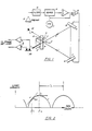
- a laser angular rate sensor having closed optical cavity ABC is shown with oppositely directed travelling waves 1 and 2 shown confined by reflective mirrors B and C and partially transmissive mirror A at the apices of the triangle.
- Two of the. mirrors, at B and C, are movable in response to the voltage output of summing amplifier 10 so as to maintain the cavity tuned to form an oscillator at the optical lasing frequency.
- the mirror 3 at A is partially transmissive to allow a processing of light from beams 1 and 2 by combiner prism 5 producing a fringe pattern on dual photodiode 20.
- Photocurrents produced in the dual photodiode 20 are amplified by dual fringe detector preamplifier 12, the outputs of which are processed to produce incremental angular output pulses in response to sensor rotation.
- Light from beam 1 is internally partially reflected at two surfaces 4 and 6 of mirror 3 and transmitted to photodiode 22, the photocurrent of which is amplified by preamp 13 and further processed to serve as a measure of cavity tuning.
- a tuned cavity produces maximum laser intensity, shown at point a on the intensity-versus-path length curve.
- a small sinusoidal modulation b of the path length produces no corresponding intensity modulation at that frequency due to the flatness of the curve at point a.
- the known approach recognizes that the same modulation c at point d on the curve produces an output e bearing the same phase as c, due to the positive slope of the curve, at point d. Were the modulation at point f, the output phase would be reversed (not shown).
- the magnitude and phase of the intensity modulation is used by the path length control loop as an error indication to cause automatic respositioning of the movable mirror 7 and/or 9 of Figure 1 to achieve an optimum operation at point a of the gain curve of Figure 2.
- oscillator 11 produces a sinusoidal voltage applied to amplifier 10 which in turn vibrates mirror 7 and/or 9. That voltage is also applied to demodulator 14 as a phase reference in the phase-sensitive demodulation of the signal at the output of preamplifier 13. Filter 15 in some implementations of path length control (PLC) loops is often not used.
- PLC path length control
- a second problem involves compromising the design of the optics to produce transmitted beams for both fringe detector and path length control functions.
- the interface at 4 must intentionally be partially reflective, thus subtracting from light transmitted into prism 4 and ultimately reducing the light flux available to illuminate fringe detector photodiode 20.
- the present invention shown in Figure 3, solves these problems using the output from dual fringe detector preamplifiers 12 to provide signals for operation of the path length control loop. This permits optimization and simplification of the optics design by removing the necessity to have a partially reflective surface at interface 4, allowing full transmitted power from beam 1 to be available in producing a fringing pattern on dual photodiode 20.
- this objective is attained by a novel detection and processing means which first algebraically combines the outputs of the fringe detector preamps, secondly, amplitude demodulates that signal. and thirdly incorporates a means by which a carrier signal near the modulation frequency is prevented from falsely perturbing the path length control loop.
- the output of the dual fringe detector preamplifier 12 consist of a pair of amplitude and phase modulated signals separated in phase by nominally 90°.
- the phase-leading signal can be expressed as where
- phase-lagging signal A x is expressed identically except that the term cosk, [--] is replaced by sink 1 [--[.
- the nominal phase separation between these signals is ordinarily achieved by adjusting the optics to produce a fringe separation related to the separation of the elements of the dual photodiode 20.
- the signals are processed in such a manner that the amplitude modulation is recovered for use as a Path Length Control (PLC) error signal while the phase / frequency information is processed as before to produce incremental angular output pulses in response to sensor rotation.
- PLC Path Length Control
- the detector circuitry 17 of Figure 3 is shown in more detail in Figure 4.
- the fringe detector preamplifier output signals are algebraically combined together in combining amplifier 31 and applied to an amplitude detector which could be of the full-wave diode bridge type 35 shown.
- Switch 33 is shown in the position which connects the output of the amplitude detector to capacitor 32 and ac amplifier 36 and then to the PLC loop filter 15 of Figure 3. Switch 33 is in this closed position when the frequency of the fringe detector signal, represented by the term
- capacitor 32 acts as a smoothing filter to the rectified carrier but allows the envelope modulation to pass on to amplifier 36.
- Figure 5(a) shows the magnitude of the frequency of the fringe detector signal, , as a function of time for a condition under which both a dither rate O d and an input rate ⁇ i of somewhat lesser value are applied. Shown as constant are the jitter frequency wj and the reference frequency w* at a somewhat larger value.
- Figure 5(b) shows the condition of the switch 33 of Figure 4. For the switch is closed, coupling the amplitude modulated signal to amplifier 36 of Figure 4.
- the frequency-phase detector provides a logic zero output when and a logic one when for actuation of the electronic switch 33.
- this detector will recognize this detector as a Type II phase/frequency detector.
- a single PLC photodiode is used in the interest of cost reduction, rather than two.
- "winking" effects intensity modulation at the optical difference frequency
- components from both beams are already present in the fringe detector signal, so “winking” effects tend to cancel.
- the present invention exhibits a great advantage in permitting simplification and optimization of the prismimirror optical system and improving the PLC control function by deriving a higher intensity control signal from the output of the fringe detector amplifiers.
Landscapes
- Physics & Mathematics (AREA)
- Engineering & Computer Science (AREA)
- Optics & Photonics (AREA)
- Electromagnetism (AREA)
- Power Engineering (AREA)
- General Physics & Mathematics (AREA)
- Radar, Positioning & Navigation (AREA)
- Remote Sensing (AREA)
- Optical Communication System (AREA)
- Lasers (AREA)
- Optical Radar Systems And Details Thereof (AREA)
- Gyroscopes (AREA)
Abstract
Description
- This invention relates generally to laser angular rate sensors and more particularly concerns an improvement in apparatus which maintains the optical path length at an integer number of wavelengths of the laser light.
- Path length control systems require a signal indicative of laser intensity. Typically this is provided by at least one photodiode and preamplifier.
- In the prior art, shown in Figure 1, a laser angular rate sensor having closed optical cavity ABC is shown with oppositely directed travelling waves 1 and 2 shown confined by reflective mirrors B and C and partially transmissive mirror A at the apices of the triangle. Two of the. mirrors, at B and C, are movable in response to the voltage output of
summing amplifier 10 so as to maintain the cavity tuned to form an oscillator at the optical lasing frequency. The mirror 3 at A is partially transmissive to allow a processing of light from beams 1 and 2 by combiner prism 5 producing a fringe pattern ondual photodiode 20. Photocurrents produced in thedual photodiode 20 are amplified by dualfringe detector preamplifier 12, the outputs of which are processed to produce incremental angular output pulses in response to sensor rotation. Light from beam 1 is internally partially reflected at twosurfaces 4 and 6 of mirror 3 and transmitted tophotodiode 22, the photocurrent of which is amplified bypreamp 13 and further processed to serve as a measure of cavity tuning. - Referring to Figure 2, a tuned cavity produces maximum laser intensity, shown at point a on the intensity-versus-path length curve. A small sinusoidal modulation b of the path length produces no corresponding intensity modulation at that frequency due to the flatness of the curve at point a. The known approach recognizes that the same modulation c at point d on the curve produces an output e bearing the same phase as c, due to the positive slope of the curve, at point d. Were the modulation at point f, the output phase would be reversed (not shown). The magnitude and phase of the intensity modulation is used by the path length control loop as an error indication to cause automatic respositioning of the movable mirror 7 and/or 9 of Figure 1 to achieve an optimum operation at point a of the gain curve of Figure 2.
- Referring again to prior art Figure 1, oscillator 11 produces a sinusoidal voltage applied to
amplifier 10 which in turn vibrates mirror 7 and/or 9. That voltage is also applied todemodulator 14 as a phase reference in the phase-sensitive demodulation of the signal at the output ofpreamplifier 13.Filter 15 in some implementations of path length control (PLC) loops is often not used. - One problem with the prior art approach lies with the small signal amplitude of the photocurrent in
photodiode 22 requiring substantial gain inpreamp 13. The small value of photocurrent results from the low level of light intensity impinging onphotodiode 22. This light is but a fraction of that transmitted through mirror 3 from beam 1. At interface 4 between mirror 3 and prism 5, the major portion of the light is transmitted into prism 5 where after three internal reflections at the prism surfaces shown, it is transmitted ontophotodiode 20 along with light directly transmitted from beam 2. The light reflected at interface 4 loses further intensity upon reflection atpoint 6 and transmission through point 8. As a result of the low intensity, the signal-to-noise ratio of the signal impinging onphotodiode 22 is degraded as is the performance of the path length control function. - A second problem involves compromising the design of the optics to produce transmitted beams for both fringe detector and path length control functions. To produce a beam to illuminate
photodiode 22, the interface at 4 must intentionally be partially reflective, thus subtracting from light transmitted into prism 4 and ultimately reducing the light flux available to illuminatefringe detector photodiode 20. - The present invention, shown in Figure 3, solves these problems using the output from dual
fringe detector preamplifiers 12 to provide signals for operation of the path length control loop. This permits optimization and simplification of the optics design by removing the necessity to have a partially reflective surface at interface 4, allowing full transmitted power from beam 1 to be available in producing a fringing pattern ondual photodiode 20. - Accordingly, it is the primary aim of the present invention to improve a detection and processing means to recover intensity modulation from the outputs of the
fringe detector preamplifiers 12. In so doing this permits the elimination ofphotodiode 22 and its associatedpreamplifier 13, shown in Figure 1. - In accordance with the present invention, this objective is attained by a novel detection and processing means which first algebraically combines the outputs of the fringe detector preamps, secondly, amplitude demodulates that signal. and thirdly incorporates a means by which a carrier signal near the modulation frequency is prevented from falsely perturbing the path length control loop.
-
- Figure 1 is a block diagram of a prior art fringe detector and path length control circuit for a laser system;
- Figure 2 is a graph of path length versus laser intensity in accordance with which the principles of intentionally acquiring and processing an optical control signal are explained;
- Figure 3 is a block diagram of the present path length control system in which the optical prism and mirror system is optimized and the control signaf is derived from the output of the fringe detector;
- Figure 4 is a schematic drawing more particularly showing the present control signal derivation circuit; and
- Figure 5 is a graph of frequency versus time for certain signals present at various points in the circuit of Figure 4, in particular:
- Figure 5(a) shows the frequency of the fringe detector signal,


- Figure 5(b) shows the status of
electronic switch 33 in time relation to Figure 5 (a); and - Figure 5(c) shows the status of
ac amplifier 36 output also in time relation to Figure 5 (a). - Referring to Figure 3, the output of the dual
fringe detector preamplifier 12 consist of a pair of amplitude and phase modulated signals separated in phase by nominally 90°. The phase-leading signal can be expressed as
- Ao = carrier signal amplitude,
- ma = degree of amplitude modulation,
- W- j = radian frequency of the amplitude modulation.
- k1 = scaling factor determined by the physical, properties of the sensor
- Ωi = input angular rate applied to the sensor, Ωd = magnitude of the dither angular rate, and
- Wd = radian frequency of the dither.
- The phase-lagging signal Ax is expressed identically except that the term cosk, [--] is replaced by sink1 [--[. The nominal phase separation between these signals is ordinarily achieved by adjusting the optics to produce a fringe separation related to the separation of the elements of the
dual photodiode 20. - In the present invention, the signals are processed in such a manner that the amplitude modulation is recovered for use as a Path Length Control (PLC) error signal while the phase/frequency information is processed as before to produce incremental angular output pulses in response to sensor rotation. The detector circuitry 17 of Figure 3 is shown in more detail in Figure 4.
- Referring to Figure 4, the fringe detector preamplifier output signals are algebraically combined together in combining
amplifier 31 and applied to an amplitude detector which could be of the full-wavediode bridge type 35 shown.Switch 33 is shown in the position which connects the output of the amplitude detector tocapacitor 32 andac amplifier 36 and then to thePLC loop filter 15 of Figure 3.Switch 33 is in this closed position when the frequency of the fringe detector signal, represented by the term -


capacitor 32 acts as a smoothing filter to the rectified carrier but allows the envelope modulation to pass on to amplifier 36. As the frequency of the fringe detector signal diminishes, it approaches the jitter frequency, a condition under which the fringe detector signal would become indistinguishable from its amplitude modulation. This condition would severely perturb the PLC loop were no measures taken. Openingswitch 33 prevents that ambiguity from occurring. Actuation ofelectronic switch 33 is by means of a frequency comparator circuit consisting offrequency reference generator 40, zerocrossing detector 43 and frequency/phase detector 47. - Operation of the frequency comparator circuit is described with the aid of Figure 5. Figure 5(a) shows the magnitude of the frequency of the fringe detector signal,

switch 33 of Figure 4. For
amplifier 36 of Figure 4. The output might appear as shown by the solid line in Figure 5(c), a condition wherein a PLC loop error signal of some magnitude exists at the jitter frequency,
capacitor 32 of Figure 4 is an input to theamplifier 36 producing a constant output. Thus, with the switch open, the fringe detector signal, when its frequency becomes near or less than the jitter frequency, is not coupled into the PLC control loop. - The frequency-phase detector provides a logic zero output when


electronic switch 33. Those skilled in the art will recognize this detector as a Type II phase/frequency detector. - The need for the zero crossing comparator arises in that the phase detector requires logic level signals which the comparator provides.
- Incorporation of the present invention into known PLC control systems will produce significant cost savings. For instance, a total of nine photodiodes are presently used in one such system, six of which are for the PLC function. Those six photodiodes and their preamplifiers and attendant installation and alignment are eliminated.
- Furthermore, in certain laser systems, a single PLC photodiode is used in the interest of cost reduction, rather than two. When two diodes are used per axis, one for each beam rotation, "winking" effects (intensity modulation at the optical difference frequency) tend to add to zero minimizing interaction with the PLC loop. However, by applying the present invention in such arrangements, components from both beams are already present in the fringe detector signal, so "winking" effects tend to cancel.
- The present invention exhibits a great advantage in permitting simplification and optimization of the prismimirror optical system and improving the PLC control function by deriving a higher intensity control signal from the output of the fringe detector amplifiers.
- Other advantages and modifications of the present arrangement are apparent to one ordinarily skilled in the art as there has been described a novel PLC control system which should only be deemed to be limited in scope by the claims which follow.
Claims (6)
Applications Claiming Priority (2)
| Application Number | Priority Date | Filing Date | Title |
|---|---|---|---|
| US07/013,080 US4781462A (en) | 1987-02-09 | 1987-02-09 | Path length control signal derivation circuit for a laser angular rate sensor |
| US13080 | 1987-02-09 |
Publications (2)
| Publication Number | Publication Date |
|---|---|
| EP0285723A2 true EP0285723A2 (en) | 1988-10-12 |
| EP0285723A3 EP0285723A3 (en) | 1989-07-26 |
Family
ID=21758209
Family Applications (1)
| Application Number | Title | Priority Date | Filing Date |
|---|---|---|---|
| EP87308528A Withdrawn EP0285723A3 (en) | 1987-02-09 | 1987-09-25 | Path length control for laser angular rate sensors |
Country Status (5)
| Country | Link |
|---|---|
| US (1) | US4781462A (en) |
| EP (1) | EP0285723A3 (en) |
| JP (1) | JPS63224280A (en) |
| AU (1) | AU7943987A (en) |
| NO (1) | NO880540L (en) |
Cited By (3)
| Publication number | Priority date | Publication date | Assignee | Title |
|---|---|---|---|---|
| FR2672986A1 (en) * | 1991-01-11 | 1992-08-21 | Litton Systems Inc | SYSTEM FOR ADJUSTING THE LENGTH OF THE CAVITY OF A RING LASER GYROSCOPE. |
| WO1995010024A1 (en) * | 1993-10-01 | 1995-04-13 | Honeywell Inc. | Path length controller for ring laser gyroscope |
| WO2006078420A1 (en) * | 2005-01-21 | 2006-07-27 | Honeywell International Inc. | Single sensor ring laser gyroscope |
Families Citing this family (1)
| Publication number | Priority date | Publication date | Assignee | Title |
|---|---|---|---|---|
| US5530542A (en) * | 1995-04-19 | 1996-06-25 | Hewlett-Packard Company | Circuit and method for controlling glitches in low intensity signals |
Citations (2)
| Publication number | Priority date | Publication date | Assignee | Title |
|---|---|---|---|---|
| US4320974A (en) * | 1980-06-30 | 1982-03-23 | The Singer Company | Pathlength controller for a ring laser cyroscope |
| US4637723A (en) * | 1982-09-30 | 1987-01-20 | Honeywell Inc. | Discriminant apparatus for ring laser angular rate sensors |
Family Cites Families (1)
| Publication number | Priority date | Publication date | Assignee | Title |
|---|---|---|---|---|
| US4551021A (en) * | 1982-03-01 | 1985-11-05 | Honeywell Inc. | Discriminant apparatus for laser gyros |
-
1987
- 1987-02-09 US US07/013,080 patent/US4781462A/en not_active Expired - Lifetime
- 1987-09-25 EP EP87308528A patent/EP0285723A3/en not_active Withdrawn
- 1987-10-07 AU AU79439/87A patent/AU7943987A/en not_active Abandoned
- 1987-10-29 JP JP62274633A patent/JPS63224280A/en active Pending
-
1988
- 1988-02-08 NO NO880540A patent/NO880540L/en unknown
Patent Citations (2)
| Publication number | Priority date | Publication date | Assignee | Title |
|---|---|---|---|---|
| US4320974A (en) * | 1980-06-30 | 1982-03-23 | The Singer Company | Pathlength controller for a ring laser cyroscope |
| US4637723A (en) * | 1982-09-30 | 1987-01-20 | Honeywell Inc. | Discriminant apparatus for ring laser angular rate sensors |
Cited By (5)
| Publication number | Priority date | Publication date | Assignee | Title |
|---|---|---|---|---|
| FR2672986A1 (en) * | 1991-01-11 | 1992-08-21 | Litton Systems Inc | SYSTEM FOR ADJUSTING THE LENGTH OF THE CAVITY OF A RING LASER GYROSCOPE. |
| WO1995010024A1 (en) * | 1993-10-01 | 1995-04-13 | Honeywell Inc. | Path length controller for ring laser gyroscope |
| US5450198A (en) * | 1993-10-01 | 1995-09-12 | Honeywell Inc. | Laser gyro microprocessor based smart mode acquisition and high performance mode hopping |
| WO2006078420A1 (en) * | 2005-01-21 | 2006-07-27 | Honeywell International Inc. | Single sensor ring laser gyroscope |
| US7330269B2 (en) | 2005-01-21 | 2008-02-12 | Honeywell International Inc. | Single sensor ring laser gyroscope |
Also Published As
| Publication number | Publication date |
|---|---|
| NO880540D0 (en) | 1988-02-08 |
| NO880540L (en) | 1988-08-10 |
| EP0285723A3 (en) | 1989-07-26 |
| US4781462A (en) | 1988-11-01 |
| AU7943987A (en) | 1988-08-11 |
| JPS63224280A (en) | 1988-09-19 |
Similar Documents
| Publication | Publication Date | Title |
|---|---|---|
| EP0189907B1 (en) | Angular rate sensor | |
| US4748686A (en) | Coherence multiplexed optical position transducer | |
| US4765739A (en) | Fiber optical rotation sensor utilizing the Sagnac phase difference | |
| EP1144950B1 (en) | System for suppression of relative intensity noise in a fiber optic gyroscope | |
| KR100210543B1 (en) | Tracking error signal generator | |
| JPS6323485B2 (en) | ||
| JPS6346367B2 (en) | ||
| KR910006658B1 (en) | Detecting apparatus of focus error | |
| US4781462A (en) | Path length control signal derivation circuit for a laser angular rate sensor | |
| US4488276A (en) | Information read apparatus with tracking control system | |
| US5116129A (en) | Digital phase ramp type fiber optic gyro | |
| US4985880A (en) | Optical information recording and reproducing apparatus | |
| US5048961A (en) | Phase modulated fiber-optic gyroscope for measuring the angular velocity of a moving object | |
| US5412472A (en) | Optical-interference type angular velocity or rate sensor having an output of improved linearity | |
| US5305084A (en) | Heterodyne interferometer | |
| GB2147695A (en) | Balancing of interferometric optical fibre sensors | |
| FR2445512A1 (en) | Position detecting system for image forming appts. - includes two part photodiode providing two signals with difference proportional to position error | |
| GB2071905A (en) | Angular velocity sensor based on a ring laser | |
| EP0332412A1 (en) | Combination fringe pattern and power monitoring assembly for a ring laser gyroscope | |
| CA2062550C (en) | Optical distance measuring apparatus | |
| CA2061904C (en) | Phase modulated fiber optic gyro accommodating angular rate reversals | |
| JPH0472163B2 (en) | ||
| US4290697A (en) | Method to eliminate fiber interferometer reflections | |
| SU1037070A1 (en) | Device for measuring linear displacements of objects | |
| JP2729290B2 (en) | Fiber optic gyro |
Legal Events
| Date | Code | Title | Description |
|---|---|---|---|
| PUAI | Public reference made under article 153(3) epc to a published international application that has entered the european phase |
Free format text: ORIGINAL CODE: 0009012 |
|
| AK | Designated contracting states |
Kind code of ref document: A2 Designated state(s): DE FR GB IT SE |
|
| PUAL | Search report despatched |
Free format text: ORIGINAL CODE: 0009013 |
|
| AK | Designated contracting states |
Kind code of ref document: A3 Designated state(s): DE FR GB IT SE |
|
| 17P | Request for examination filed |
Effective date: 19900122 |
|
| 17Q | First examination report despatched |
Effective date: 19910214 |
|
| STAA | Information on the status of an ep patent application or granted ep patent |
Free format text: STATUS: THE APPLICATION IS DEEMED TO BE WITHDRAWN |
|
| 18D | Application deemed to be withdrawn |
Effective date: 19910827 |
|
| RIN1 | Information on inventor provided before grant (corrected) |
Inventor name: WEITZNER, MARK A. Inventor name: FERRISS, LINCOLN S. |