EP0285493B1 - Apparatus for testing light-emitting devices - Google Patents
Apparatus for testing light-emitting devices Download PDFInfo
- Publication number
- EP0285493B1 EP0285493B1 EP88400668A EP88400668A EP0285493B1 EP 0285493 B1 EP0285493 B1 EP 0285493B1 EP 88400668 A EP88400668 A EP 88400668A EP 88400668 A EP88400668 A EP 88400668A EP 0285493 B1 EP0285493 B1 EP 0285493B1
- Authority
- EP
- European Patent Office
- Prior art keywords
- light
- probe
- emitting devices
- fiber
- casing
- Prior art date
- Legal status (The legal status is an assumption and is not a legal conclusion. Google has not performed a legal analysis and makes no representation as to the accuracy of the status listed.)
- Expired - Lifetime
Links
- 238000012360 testing method Methods 0.000 title claims description 62
- 239000000523 sample Substances 0.000 claims description 48
- 239000000835 fiber Substances 0.000 claims description 25
- 230000003287 optical effect Effects 0.000 claims description 16
- 230000006870 function Effects 0.000 claims description 8
- 230000003247 decreasing effect Effects 0.000 claims description 3
- 230000000717 retained effect Effects 0.000 claims 1
- 238000010586 diagram Methods 0.000 description 6
- 238000005253 cladding Methods 0.000 description 2
- 238000000034 method Methods 0.000 description 2
- 239000013307 optical fiber Substances 0.000 description 2
- 238000006243 chemical reaction Methods 0.000 description 1
- 230000008878 coupling Effects 0.000 description 1
- 238000010168 coupling process Methods 0.000 description 1
- 238000005859 coupling reaction Methods 0.000 description 1
- 238000006073 displacement reaction Methods 0.000 description 1
- 230000000694 effects Effects 0.000 description 1
- 230000003760 hair shine Effects 0.000 description 1
- 239000000787 lecithin Substances 0.000 description 1
- 238000012544 monitoring process Methods 0.000 description 1
- 230000008569 process Effects 0.000 description 1
- 238000011946 reduction process Methods 0.000 description 1
Images


Classifications
-
- G—PHYSICS
- G09—EDUCATION; CRYPTOGRAPHY; DISPLAY; ADVERTISING; SEALS
- G09G—ARRANGEMENTS OR CIRCUITS FOR CONTROL OF INDICATING DEVICES USING STATIC MEANS TO PRESENT VARIABLE INFORMATION
- G09G3/00—Control arrangements or circuits, of interest only in connection with visual indicators other than cathode-ray tubes
- G09G3/006—Electronic inspection or testing of displays and display drivers, e.g. of LED or LCD displays
-
- G—PHYSICS
- G01—MEASURING; TESTING
- G01J—MEASUREMENT OF INTENSITY, VELOCITY, SPECTRAL CONTENT, POLARISATION, PHASE OR PULSE CHARACTERISTICS OF INFRARED, VISIBLE OR ULTRAVIOLET LIGHT; COLORIMETRY; RADIATION PYROMETRY
- G01J1/00—Photometry, e.g. photographic exposure meter
- G01J1/02—Details
- G01J1/04—Optical or mechanical part supplementary adjustable parts
- G01J1/0407—Optical elements not provided otherwise, e.g. manifolds, windows, holograms, gratings
- G01J1/0425—Optical elements not provided otherwise, e.g. manifolds, windows, holograms, gratings using optical fibers
-
- G—PHYSICS
- G01—MEASURING; TESTING
- G01J—MEASUREMENT OF INTENSITY, VELOCITY, SPECTRAL CONTENT, POLARISATION, PHASE OR PULSE CHARACTERISTICS OF INFRARED, VISIBLE OR ULTRAVIOLET LIGHT; COLORIMETRY; RADIATION PYROMETRY
- G01J1/00—Photometry, e.g. photographic exposure meter
- G01J1/42—Photometry, e.g. photographic exposure meter using electric radiation detectors
- G01J2001/4247—Photometry, e.g. photographic exposure meter using electric radiation detectors for testing lamps or other light sources
- G01J2001/4252—Photometry, e.g. photographic exposure meter using electric radiation detectors for testing lamps or other light sources for testing LED's
-
- G—PHYSICS
- G01—MEASURING; TESTING
- G01R—MEASURING ELECTRIC VARIABLES; MEASURING MAGNETIC VARIABLES
- G01R31/00—Arrangements for testing electric properties; Arrangements for locating electric faults; Arrangements for electrical testing characterised by what is being tested not provided for elsewhere
- G01R31/26—Testing of individual semiconductor devices
- G01R31/2607—Circuits therefor
- G01R31/2632—Circuits therefor for testing diodes
- G01R31/2635—Testing light-emitting diodes, laser diodes or photodiodes
Definitions
- the present invention relates to the optical testing of light-emitting devices and displays. More specifically, the invention relates to a test apparatus which may be used, in conjunction with conventional automatic test equipment, to optically test a variety of light-emitting devices.
- ATE automatic test equipment
- a printed circuit board which contains a variety of discrete components, integrated circuits and other devices may be subjected to comprehensive electrical testing by means of a "bed of nails" test fixture.
- Printed circuit boards frequently include light-emitting components such as light-emitting diodes, seven-segment displays and the like, which must be tested both electrically and optically.
- Optical testing may determine whether a component is actually emitting light when it should be, whether the emission exceeds a minimum acceptable intensity, whether the intensities among several components are sufficiently uniform, etc.
- One technique of optically testing light-emitting devices involves a machine vision system in which a television camera is aimed at a light-emitting device under test (DUT).
- the image produced by the camera provides information on emitter intensity and background intensity on a pixel-by-pixel basis.
- An analog-to-digital conversion is then performed and the equivalent binary values are stored in memory.
- the output signals provided by the vision system are typically not electrically compatible with conventional ATE inputs, thus preventing a direct connection of the vision system with an ATE host.
- the optical testing of the DUT cannot be directly combined with the electrical testing into a common automatic test program.
- the vision system produces large amounts of data which are not useful.
- the object of the test is to determine simply whether a particular light-emitting device is illuminated at a particular time.
- the DUT is a printed circuit board which contains several widely spaced light-emitting diodes and that the viewing angle of the camera is wide enough to cover the entire surface of the circuit board.
- most of the pixels in the image produced by the camera will not be of the diodes themselves and are therefore not of interest.
- most of the corresponding binary data is irrelevant and a data reduction process must be performed, which typically requires complex image processing software.
- the camera provides a fixed, uniform spatial resolution across its entire field of view. This may represent a significant disadvantage in cases where the DUT contains several widely spaced clusters of closely spaced light-emitting devices.
- the vision system may require additional cameras, thereby increasing the cost and complexity of the system.
- the cost of the vision system is relatively high due to the necessity of the camera(s), the large memory required to store the data and the image processing software.
- JP-A-60025244 discloses a single probe for testing light-emitting diodes on an integrated circuit wafer.
- the probe includes an optical fiber and is connected to a current source such that when the probe makes contact with a diode, current is applied to forward bias and turn on the diode.
- the optical fiber carries light emitted by a diode to a photodetector, whose output is connected to a signal processor.
- Document FR-A-2,512,217 discloses a optocoupler and modular housing for coupling light from light-emitting components on a printed circuit board.
- a separate device for making an electrical connection with the printed circuit board may also be placed in the same housing with the optocoupler.
- the present invention provides a test fixture which may be used in conjunction with conventional automatic test equipment to perform optical testing of a wide variety of light-emitting devices.
- the invention comprises an apparatus for optically testing a plurality of light-emitting devices arranged on a device under test in a preselected pattern, wherein said apparatus includes a retaining means for securing a plurality of probe means in preselected locations corresponding to said preselected pattern such that each of said probe means may optically test one of said light-emitting devices, each of said probe means including a light-emitting fiber disposed in a casing and a detector means, said fiber having a first end for receiving light and a second end coupled to said detector means, one or more of said probe means has have a selectively variable angle of acceptance, whereby the field of view of each probe means is individually adjusted to receive light from a predetermined one of said plurality of light-emitting devices and to substantially exclude light emitted from other light-emitting devices, and said apparatus is adapted to interface with automatic test equipment, whereby said automatic test equipment is programmable to automatically test the optical functions of said light-emitting devices.
- Each probe is therefore disposed in close proximity to a light-emitting component and a fiber optic cable connects each probe to a detector.
- Each of the detectors provides an electrical output signal which is related to the intensity of the light conducted by its fiber optic cable.
- the output signals of the detectors are electrically compatible with conventional ATE inputs and may be directly connected thereto.
- Each detector may be individually calibrated.
- Each probe may be mounted in a fixed position or, alternatively, may be provided with a telescopic capability, whereby a DUT having light-emitting components of varying heights may be accommodated.
- the light-conducting fiber within each fiber optic cable may be recessed with respect to its casing, thereby effectively decreasing its acceptance angle. As a result, the spatial resolution of the test fixture may be adjusted on a probe-by-probe basis.
- the present invention provides additional advantages over a conventional vision system. For example, since each light-emitting component under test is paired with an individual probe, the need for a camera is eliminated. Moreover, because each probe is directed to a specific light-emitting component, as opposed to an area which may contain numerous components, the present invention produces data with respect to the light-emitting components only. Thus, by eliminating large quantities of irrelevant data, the present invention also eliminates the need for a large memory to store such data and the complex software required to process the data.
- test fixture and probe are low in cost and simple to construct.
- the test fixture is durable and is easy to operate.
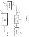
- FIG. 1 is a block diagram of a system known in the prior art for automatically testing the electrical functions of a given device.
- An automatic test unit 2 provides a plurality of output lines 4 which are connected to a plurality of drivers 6.
- the drivers 6 are in turn connected by a plurality of probes 8 to a device under test (DUT) 10.
- a plurality of probes 12 connects the DUT 10 to a plurality of electrical sensors 14.
- the sensors 14 provide a plurality of output lines 16 which are connected to the test unit 2.
- the test unit 2 may be programmed to automatically perform a series of electrical tests on the DUT 10.
- the sensors 14 monitor the areas of interest on the DUT and provide data to the test unit 2.
- the sensors 14, however, are generally responsive only to electrical signals and are not capable of sensing optical signals which may be produced by light-emitting components of the DUT 10.
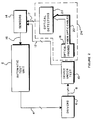
- FIG. 2 is a block diagram of a system for optically testing one or more light-emitting devices.
- An optical test fixture 24 comprises one or more optical probes 18, each of which is connected to an optical detector 22 by a fiber optic cable 20.
- the probes 18 are disposed in close proximity to the DUT 10, whereby light emitted by components thereon may be conducted along the fiber optic cables 20 to the detectors 22.
- Output lines 17 of the detectors 22 are connected to the sensors 14.
- the optical functions of the DUT 10 may be automatically tested by the test unit 2 in a manner similar to that discussed above.
- Figure 3 is an elevational view of the test fixture 24 shown in Figure 2.
- a pinch plate 27 is disposed upon a retaining plate 26.
- Two fasteners 29 extend through the pinch plate 27 to the retaining plate 26.
- Two pins 31 extend upward from the DUT 10.
- Two bushings 33 extend downward from the bottom of the retaining plate 26.
- a plurality of bores 28 extend through both of the plates 26 and 27.
- the bores 28 are arranged in a preselected pattern which corresponds with the arrangement of several light-emitting components 30, 32 and 34.
- An optical probe 18 is disposed in each of the bores 28.
- Each probe 18 comprises a fiber optic cable 20.
- Each cable 20 extends upward from the pinch plate 27 into a bore 38, which is disposed in a support member 36.
- a detector 22 is disposed adjacent to each of the bores 38 and is coupled to the end of the cable 20 disposed therein.
- a lead 40 extends from each of the detectors 22 to a multi-pin connector 42.
- the connector 42 thus provides an interface to the test fixture 24.
- a connector 44 which is shaped to mate with the connector 42, serves to connect the test fixture 24 to the sensors 14 via lines 17 ( Figure 2).
- Each of the fasteners 29 may comprise, for example, a screw disposed in a slot, whereby when the screw is loosened, the pinch plate 27 may slide laterally with respect to the retaining plate 26.
- a lateral force is imposed upon the probes 18. This lateral force tends to retain the probes 18 in their correct respective positions.
- the operation of the test fixture 24 may be summarized as follows. First, the retaining plate 26 is placed in close proximity to the DUT 10. The pins 31 engage the bushings 33, thereby ensuring correct alignment or registration of the retaining plate 26 with the DUT 10. As a result, the probes 18 are placed in close proximity to the light-emitting components 30, 32 and 34, thereby permitting the probes to receive light emitted by the components.
- the test unit 2 in accordance with its programming, controls the drivers 6, which in turn cause the DUT 10 to run through a series of preselected conditions or states. During certain ones of the preselected states, one or more of the light-emitting components 30, 32 or 34 may be illuminated. The probe 18 which corresponds to the illuminated component will conduct a portion of the emitted light along its fiber optic cable 20 to the corresponding detector 22.
- the detector 22 produces an electrical output signal whose magnitude is indicative of the intensity of the light received.
- the output signal is conducted along the lead 40 and one of the lines 17 to the corresponding sensor 14.
- the test unit 2 may determine whether a particular light-emitting component is actually illuminated when it should be, whether the component is providing a minimum brightness, whether two or more components are of uniform brightness, etc.
- one or more of the probes may comprise a telescopic feature, as depicted in Figures 4A-4E.
- the fiber optic cable 20 comprises a light-conducting inner core 50, which is surrounded by an outer cladding 49 and a jacket or casing 48.
- One end of the fiber optic cable 20 is inserted through a cylindrical sleeve 52.
- the sleeve 52 may be secured to the jacket 48, for example, by two crimps 54.
- the portion of the fiber optic cable 20 which extends below the sleeve 52 may be subsequently trimmed to a desired length.
- the free end of the fiber optic cable 20 is inserted through a spring 56, whereby the spring is disposed above and adjacent to the sleeve 52. Subsequently, the cable 20 (along with the sleeve 52 and spring 56) is inserted through a second sleeve 58. A crimp 60, disposed in the upper portion of the sleeve 58, serves to prevent upward movement of the spring 56.
- a retaining ring 62 is slid onto the free end of the fiber optic cable 20 and disposed adjacent to the sleeve 58.
- the retaining ring 62 is secured to the jacket 48 by a crimp 64, thereby restricting the downward movement of the sleeve 52 and the cable 20.
- each individual probe 18 may be extended or retracted to accommodate a device under test which contains light-emitting components of varying height.
- the light-conducting inner core 50 may be selectively recessed within the jacket 48.
- the effect of recessing the inner core 50 is that the acceptance angle of the probe 18 is decreased.
- the spatial resolution of the test fixture 24 may be advantageously altered on a probe-by-probe basis. For example, if several light-emitting components are located very close to each other, the acceptance angles of the corresponding probes may be adjusted to prevent one probe from receiving light emitted by an adjacent component.
- FIG 5 is a schematic diagram of the detector 22 shown in Figure 3.
- Two transistors 66 and 68 are arranged in a Darlington pair configuration.
- Transistor 68 is a photo-sensitive transistor.
- a load resistance 70 is connected between the emitter of the transistor 66 and ground potential.
- the end of the fiber optic cable 20 is disposed in close proximity to the collector-base junction of the transistor 68.
- the lead 40 may be connected directly to an electrical sensor 14.
- an output signal V o is produced.
- the magnitude of the output signal V o is indicative of the magnitude of the light intensity received by the transistor 68.
- the combination of transistors 66 and 68 is available as a discrete component such as Motorola part MFOD-73, which includes a connector for attaching the fiber optic cable 20.
- the load resistance 70 may comprise, for example, a discrete resistor or a rheostat. If a rheostat is used, each detector 22 may be individually calibrated by simply placing the probe 18 in close proximity to a calibrated light source, and then adjusting the rheostat to set the output signal V o at a predetermined level.
Landscapes
- Physics & Mathematics (AREA)
- General Physics & Mathematics (AREA)
- Engineering & Computer Science (AREA)
- Spectroscopy & Molecular Physics (AREA)
- Computer Hardware Design (AREA)
- Theoretical Computer Science (AREA)
- Testing Of Optical Devices Or Fibers (AREA)
- Tests Of Electronic Circuits (AREA)
Description
- The present invention relates to the optical testing of light-emitting devices and displays. More specifically, the invention relates to a test apparatus which may be used, in conjunction with conventional automatic test equipment, to optically test a variety of light-emitting devices.
- As a result of the advent of automatic test equipment (ATE), the testing of the electrical functions of complex devices has become highly automated. For example, a printed circuit board which contains a variety of discrete components, integrated circuits and other devices may be subjected to comprehensive electrical testing by means of a "bed of nails" test fixture. Printed circuit boards, however, frequently include light-emitting components such as light-emitting diodes, seven-segment displays and the like, which must be tested both electrically and optically. Optical testing may determine whether a component is actually emitting light when it should be, whether the emission exceeds a minimum acceptable intensity, whether the intensities among several components are sufficiently uniform, etc.
- One technique of optically testing light-emitting devices involves a machine vision system in which a television camera is aimed at a light-emitting device under test (DUT). The image produced by the camera provides information on emitter intensity and background intensity on a pixel-by-pixel basis. An analog-to-digital conversion is then performed and the equivalent binary values are stored in memory.
- The disadvantages of this type of vision system are numerous. First, the output signals provided by the vision system are typically not electrically compatible with conventional ATE inputs, thus preventing a direct connection of the vision system with an ATE host. As a result, the optical testing of the DUT cannot be directly combined with the electrical testing into a common automatic test program.
- Second, for certain types of optical testing, the vision system produces large amounts of data which are not useful. For example, assume that the object of the test is to determine simply whether a particular light-emitting device is illuminated at a particular time. Assume also that the DUT is a printed circuit board which contains several widely spaced light-emitting diodes and that the viewing angle of the camera is wide enough to cover the entire surface of the circuit board. Under these conditions, most of the pixels in the image produced by the camera will not be of the diodes themselves and are therefore not of interest. Moreover, most of the corresponding binary data is irrelevant and a data reduction process must be performed, which typically requires complex image processing software.
- Third, the camera provides a fixed, uniform spatial resolution across its entire field of view. This may represent a significant disadvantage in cases where the DUT contains several widely spaced clusters of closely spaced light-emitting devices. In order to resolve two adjacent light-emitting devices while also monitoring the entire DUT, the vision system may require additional cameras, thereby increasing the cost and complexity of the system.
- Finally, the cost of the vision system is relatively high due to the necessity of the camera(s), the large memory required to store the data and the image processing software.
- Document Patent Abstracts of Japan, Vol. 9, Nr. 143 [E-322] & JP-A-60025244 discloses a single probe for testing light-emitting diodes on an integrated circuit wafer. The probe includes an optical fiber and is connected to a current source such that when the probe makes contact with a diode, current is applied to forward bias and turn on the diode. The optical fiber carries light emitted by a diode to a photodetector, whose output is connected to a signal processor.
- Document FR-A-2,512,217 discloses a optocoupler and modular housing for coupling light from light-emitting components on a printed circuit board. A separate device for making an electrical connection with the printed circuit board may also be placed in the same housing with the optocoupler.
- The present invention provides a test fixture which may be used in conjunction with conventional automatic test equipment to perform optical testing of a wide variety of light-emitting devices.
- More specifically, the invention comprises an apparatus for optically testing a plurality of light-emitting devices arranged on a device under test in a preselected pattern, wherein said apparatus includes a retaining means for securing a plurality of probe means in preselected locations corresponding to said preselected pattern such that each of said probe means may optically test one of said light-emitting devices, each of said probe means including a light-emitting fiber disposed in a casing and a detector means, said fiber having a first end for receiving light and a second end coupled to said detector means, one or more of said probe means has have a selectively variable angle of acceptance, whereby the field of view of each probe means is individually adjusted to receive light from a predetermined one of said plurality of light-emitting devices and to substantially exclude light emitted from other light-emitting devices, and said apparatus is adapted to interface with automatic test equipment, whereby said automatic test equipment is programmable to automatically test the optical functions of said light-emitting devices.
- Each probe is therefore disposed in close proximity to a light-emitting component and a fiber optic cable connects each probe to a detector. Each of the detectors provides an electrical output signal which is related to the intensity of the light conducted by its fiber optic cable. The output signals of the detectors are electrically compatible with conventional ATE inputs and may be directly connected thereto. Each detector may be individually calibrated.
- Each probe may be mounted in a fixed position or, alternatively, may be provided with a telescopic capability, whereby a DUT having light-emitting components of varying heights may be accommodated. In addition, the light-conducting fiber within each fiber optic cable may be recessed with respect to its casing, thereby effectively decreasing its acceptance angle. As a result, the spatial resolution of the test fixture may be adjusted on a probe-by-probe basis.
- The present invention provides additional advantages over a conventional vision system. For example, since each light-emitting component under test is paired with an individual probe, the need for a camera is eliminated. Moreover, because each probe is directed to a specific light-emitting component, as opposed to an area which may contain numerous components, the present invention produces data with respect to the light-emitting components only. Thus, by eliminating large quantities of irrelevant data, the present invention also eliminates the need for a large memory to store such data and the complex software required to process the data.
- Both the test fixture and probe are low in cost and simple to construct. The test fixture is durable and is easy to operate.
- This invention is pointed out with particularity in the appended claims. The above and further advantages of this invention may be better understood by referring to the following description taken in conjunction with the accompanying drawings, in which:
- Figure 1 is a functional block diagram of a system known in the prior art for automatically testing the electrical functions of a device under test;
- Figure 2 is a functional block diagram of a system for automatically testing the optical functions of one or more light-emitting devices;
- Figure 3 is an elevational view of an optical test apparatus constructed in accordance with the preferred embodiment of the present invention;
- Figures 4A-4E are a series of cross-sectional views showing the assembly of a telescopic probe; and
- Figure 5 is a circuit diagram of the detector shown in Figure 3.
- Figure 1 is a block diagram of a system known in the prior art for automatically testing the electrical functions of a given device. An
automatic test unit 2 provides a plurality ofoutput lines 4 which are connected to a plurality ofdrivers 6. Thedrivers 6 are in turn connected by a plurality ofprobes 8 to a device under test (DUT) 10. A plurality ofprobes 12 connects theDUT 10 to a plurality ofelectrical sensors 14. Thesensors 14 provide a plurality ofoutput lines 16 which are connected to thetest unit 2. - In general, the
test unit 2 may be programmed to automatically perform a series of electrical tests on theDUT 10. Thesensors 14 monitor the areas of interest on the DUT and provide data to thetest unit 2. Thesensors 14, however, are generally responsive only to electrical signals and are not capable of sensing optical signals which may be produced by light-emitting components of theDUT 10. - Figure 2 is a block diagram of a system for optically testing one or more light-emitting devices. For consistency, components which are similar to those shown in Figure 1 retain the same reference numerals. An
optical test fixture 24 comprises one or moreoptical probes 18, each of which is connected to anoptical detector 22 by afiber optic cable 20. Theprobes 18 are disposed in close proximity to theDUT 10, whereby light emitted by components thereon may be conducted along thefiber optic cables 20 to thedetectors 22.Output lines 17 of thedetectors 22 are connected to thesensors 14. As a result, the optical functions of theDUT 10 may be automatically tested by thetest unit 2 in a manner similar to that discussed above. - Figure 3 is an elevational view of the
test fixture 24 shown in Figure 2. Apinch plate 27 is disposed upon a retainingplate 26. Twofasteners 29 extend through thepinch plate 27 to the retainingplate 26. Twopins 31 extend upward from theDUT 10. Twobushings 33 extend downward from the bottom of the retainingplate 26. - A plurality of
bores 28 extend through both of theplates bores 28 are arranged in a preselected pattern which corresponds with the arrangement of several light-emittingcomponents optical probe 18 is disposed in each of thebores 28. Eachprobe 18 comprises afiber optic cable 20. Eachcable 20 extends upward from thepinch plate 27 into abore 38, which is disposed in asupport member 36. Adetector 22 is disposed adjacent to each of thebores 38 and is coupled to the end of thecable 20 disposed therein. A lead 40 extends from each of thedetectors 22 to amulti-pin connector 42. Theconnector 42 thus provides an interface to thetest fixture 24. Aconnector 44, which is shaped to mate with theconnector 42, serves to connect thetest fixture 24 to thesensors 14 via lines 17 (Figure 2). - Each of the
fasteners 29 may comprise, for example, a screw disposed in a slot, whereby when the screw is loosened, thepinch plate 27 may slide laterally with respect to the retainingplate 26. By imparting a slight lateral displacement of thepinch plate 27 with respect to the retainingplate 26 and then tightening thefasteners 29, a lateral force is imposed upon theprobes 18. This lateral force tends to retain theprobes 18 in their correct respective positions. - The operation of the
test fixture 24 may be summarized as follows. First, the retainingplate 26 is placed in close proximity to theDUT 10. Thepins 31 engage thebushings 33, thereby ensuring correct alignment or registration of the retainingplate 26 with theDUT 10. As a result, theprobes 18 are placed in close proximity to the light-emittingcomponents test unit 2, in accordance with its programming, controls thedrivers 6, which in turn cause theDUT 10 to run through a series of preselected conditions or states. During certain ones of the preselected states, one or more of the light-emittingcomponents probe 18 which corresponds to the illuminated component will conduct a portion of the emitted light along itsfiber optic cable 20 to the correspondingdetector 22. - The
detector 22 produces an electrical output signal whose magnitude is indicative of the intensity of the light received. The output signal is conducted along thelead 40 and one of thelines 17 to the correspondingsensor 14. By comparing the output signals received from thevarious sensors 14 to a preselected reference, thetest unit 2 may determine whether a particular light-emitting component is actually illuminated when it should be, whether the component is providing a minimum brightness, whether two or more components are of uniform brightness, etc. - As an alternative to mounting the
probes 18 in fixed positions, one or more of the probes may comprise a telescopic feature, as depicted in Figures 4A-4E. Thefiber optic cable 20 comprises a light-conductinginner core 50, which is surrounded by anouter cladding 49 and a jacket orcasing 48. One end of thefiber optic cable 20 is inserted through acylindrical sleeve 52. Thesleeve 52 may be secured to thejacket 48, for example, by twocrimps 54. The portion of thefiber optic cable 20 which extends below thesleeve 52 may be subsequently trimmed to a desired length. As shown in Figures 4B and 4C, the free end of thefiber optic cable 20 is inserted through aspring 56, whereby the spring is disposed above and adjacent to thesleeve 52. Subsequently, the cable 20 (along with thesleeve 52 and spring 56) is inserted through asecond sleeve 58. Acrimp 60, disposed in the upper portion of thesleeve 58, serves to prevent upward movement of thespring 56. - As shown in Figure 4D, a retaining
ring 62 is slid onto the free end of thefiber optic cable 20 and disposed adjacent to thesleeve 58. The retainingring 62 is secured to thejacket 48 by acrimp 64, thereby restricting the downward movement of thesleeve 52 and thecable 20. - When an upward force is applied to the bottom of the
probe 18, thecable 20 andsleeve 52 move upward, thereby retracting the probe and compressing thespring 56. When the force is removed, thespring 56 tends to restore theprobe 18 to its extended position. Thus, as shown in Figure 4E, once the assembledprobe 18 is disposed in the retainingplate 26, eachindividual probe 18 may be extended or retracted to accommodate a device under test which contains light-emitting components of varying height. - The light-conducting
inner core 50, along with theouter cladding 49, may be selectively recessed within thejacket 48. The effect of recessing theinner core 50 is that the acceptance angle of theprobe 18 is decreased. In other words, when theinner core 50 is recessed, it "sees" or accepts light from a narrower field-of-view than it otherwise would. As a result, the spatial resolution of thetest fixture 24 may be advantageously altered on a probe-by-probe basis. For example, if several light-emitting components are located very close to each other, the acceptance angles of the corresponding probes may be adjusted to prevent one probe from receiving light emitted by an adjacent component. - Figure 5 is a schematic diagram of the
detector 22 shown in Figure 3. Twotransistors Transistor 68 is a photo-sensitive transistor. Aload resistance 70 is connected between the emitter of thetransistor 66 and ground potential. The end of thefiber optic cable 20 is disposed in close proximity to the collector-base junction of thetransistor 68. Thelead 40 may be connected directly to anelectrical sensor 14. - When light conducted by the
fiber optic cable 20 shines on thetransistor 68, an output signal Vo is produced. The magnitude of the output signal Vo is indicative of the magnitude of the light intensity received by thetransistor 68. - The combination of
transistors fiber optic cable 20. Theload resistance 70 may comprise, for example, a discrete resistor or a rheostat. If a rheostat is used, eachdetector 22 may be individually calibrated by simply placing theprobe 18 in close proximity to a calibrated light source, and then adjusting the rheostat to set the output signal Vo at a predetermined level.
Claims (7)
- An apparatus for optically testing (24) a plurality of light-emitting devices (30, 32, 34) arranged on a device unter test (DUT) in a preselected pattern, wherein:- said apparatus includes a retaining means (26, 27) for securing a plurality of probe means (18) in preselected locations corresponding to said preselected pattern such that each of said probe means may optically test one of said light-emitting devices,- each of said probe means includes a light-conducting fiber (50) disposed in a casing (48) and a detector means (22), said fiber having a first end for receiving light and a second end coupled to said detector means,- one or more of said probe means has have a selectively variable angle of acceptance, whereby the field of view of each probe means is individually adjusted to receive light from a predetermined one of said plurality of light-emitting devices and to substantially exclude light emitted from other light-emitting devices,- said apparatus is adapted to interface with automatic test equipment (ATE), whereby said automatic test equipment (ATE) is programmable to automatically test the optical functions of said light-emitting devices.
- The apparatus as in claim 1, wherein one or more of said probe means is are telescopic and comprise(s) a spring (56) surrounding said casing (48) and spaced from said first end of said fiber, a first sleeve (52) disposed between said spring and said first end of said fiber and secured to said casing, a second sleeve (58) surrounding said spring and a portion of said first sleeve and including a crimp (60) for preventing movement of the spring along said casing in a direction away from said first end, and a retaining ring (62) surrounding and secured by another crimp (64) to said casing adjacent to the end of said second sleeve which is distal from the first end of said fiber.
- The apparatus as in claim 1, wherein said retaining means comprises a first plate means (26), said first plate having a plurality of apertures for holding one or more of said probe means.
- The apparatus as in claim 3, wherein said retaining means further comprises a second plate means (27), said second plate means disposed adjacent to said first plate means and having a plurality of apertures which correspond to the apertures in said first plate means, said second plate means including one or more fastening means (29) for securing said second plate means to said first plate means, whereby said plurality of probe means are retained in substantially fixed positions.
- The apparatus as in claim 1, wherein said detector means includes means for calibrating said output signal.
- The apparatus as in claim 1, wherein said automatic test equipment (ATE) is programmable to automatically test the optical functions and to perform electrical tests on said device under test.
- The apparatus as in claim 1, wherein the light-conducting fiber in one or more of said probes is recessed within said casing, thereby decreasing the angle of acceptance of said light-conducting fiber.
Applications Claiming Priority (2)
| Application Number | Priority Date | Filing Date | Title |
|---|---|---|---|
| US07/029,451 US4808815A (en) | 1987-03-23 | 1987-03-23 | Apparatus for testing light-emitting devices using probe means having a preselected pattern arrangement |
| US29451 | 1987-03-23 |
Publications (3)
| Publication Number | Publication Date |
|---|---|
| EP0285493A2 EP0285493A2 (en) | 1988-10-05 |
| EP0285493A3 EP0285493A3 (en) | 1990-12-27 |
| EP0285493B1 true EP0285493B1 (en) | 1995-04-26 |
Family
ID=21849069
Family Applications (1)
| Application Number | Title | Priority Date | Filing Date |
|---|---|---|---|
| EP88400668A Expired - Lifetime EP0285493B1 (en) | 1987-03-23 | 1988-03-21 | Apparatus for testing light-emitting devices |
Country Status (4)
| Country | Link |
|---|---|
| US (1) | US4808815A (en) |
| EP (1) | EP0285493B1 (en) |
| JP (1) | JP2755952B2 (en) |
| DE (1) | DE3853644T2 (en) |
Cited By (1)
| Publication number | Priority date | Publication date | Assignee | Title |
|---|---|---|---|---|
| WO2003100448A1 (en) * | 2002-05-28 | 2003-12-04 | Compusign Pty Ltd | Array monitoring |
Families Citing this family (41)
| Publication number | Priority date | Publication date | Assignee | Title |
|---|---|---|---|---|
| US5134280A (en) * | 1990-05-21 | 1992-07-28 | Everett/Charles Contact Products, Inc. | Optical fiber test probe having a sleeve-like plunger movable in a barrel |
| US5317656A (en) * | 1991-05-17 | 1994-05-31 | Texas Instruments Incorporated | Fiber optic network for multi-point emissivity-compensated semiconductor wafer pyrometry |
| DE4119109A1 (en) * | 1991-06-10 | 1992-12-17 | Grundig Emv | METHOD FOR TESTING DISPLAY COMPONENTS AND ARRANGEMENT FOR IMPLEMENTING THE METHOD |
| US5630001A (en) * | 1995-05-22 | 1997-05-13 | Motorola | Image generator for use in image manifestation apparatus |
| US5956447A (en) * | 1996-05-07 | 1999-09-21 | Univ Central Florida | Device and method for image acquisition through multi-mode fiber |
| GB9824671D0 (en) * | 1998-11-11 | 1999-01-06 | Cashmaster Int Ltd | Monitoring apparatus |
| IES20000322A2 (en) * | 2000-04-28 | 2001-11-14 | Viveen Ltd | Apparatus for testing a light source |
| US6597195B1 (en) * | 2000-07-28 | 2003-07-22 | Labsphere, Inc. | Method of and cassette structure for burn-in and life testing of multiple LEDs and the like |
| DE10048447B4 (en) * | 2000-09-29 | 2006-05-18 | Premosys Gmbh | Method and device for testing self-luminous optoelectronic components |
| US6490037B1 (en) * | 2000-11-13 | 2002-12-03 | Test Coach Corporation | Method and apparatus for verifying a color of an LED in a printed circuit board |
| US6493077B1 (en) * | 2001-07-16 | 2002-12-10 | International Business Machines Corporation | Optical test probe for silicon optical bench |
| US7302382B2 (en) * | 2002-02-20 | 2007-11-27 | Xerox Corporation | Generating with lexical functional grammars |
| US7129722B1 (en) * | 2002-10-09 | 2006-10-31 | Cypress Semiconductor Corp. | Methods of improving reliability of an electro-optical module |
| US20040135595A1 (en) * | 2002-10-30 | 2004-07-15 | Finisar Corporation | Methods, systems, and devices for burn-in testing of optoelectronic devices |
| US6956226B2 (en) * | 2003-01-15 | 2005-10-18 | Hewlett-Packard Development Company, L.P. | Light image sensor test of opto-electronics for in-circuit test |
| US7064832B2 (en) * | 2003-02-26 | 2006-06-20 | Delaware Capital Formation, Inc. | Color and intensity measuring module for test of light emitting components by automated test equipment |
| US7023554B2 (en) * | 2003-11-14 | 2006-04-04 | Test Coach Corporation | Method and apparatus for determining a color and brightness of an LED in a printed circuit board |
| US7348786B2 (en) * | 2004-08-31 | 2008-03-25 | Georgia Tech Research Corporation | Probe module for testing chips with electrical and optical input/output interconnects, methods of use, and methods of fabrication |
| US7265822B2 (en) * | 2004-10-01 | 2007-09-04 | Test Coach Corporation | Method and apparatus for determining presence of a component in a printed circuit board |
| US20060214089A1 (en) * | 2005-03-22 | 2006-09-28 | An Byoung E | Method and apparatus for real time output monitoring of light sources and flexible sensitivity adjustment of light sensors |
| CN100573168C (en) * | 2005-04-21 | 2009-12-23 | 鸿富锦精密工业(深圳)有限公司 | The system and method for test computer panel LED light lamp and connecting line thereof |
| CN101169340B (en) * | 2006-10-27 | 2010-12-08 | 鸿富锦精密工业(深圳)有限公司 | Motherboard light-emitting diode detection device and method |
| TWI390194B (en) * | 2006-11-10 | 2013-03-21 | Hon Hai Prec Ind Co Ltd | Device and method for testing leds on a motherboard |
| CN101424722B (en) * | 2007-10-31 | 2011-01-05 | 鸿富锦精密工业(深圳)有限公司 | Motherboard light-emitting diode testing system and method |
| JP5314634B2 (en) * | 2010-05-17 | 2013-10-16 | 株式会社アドバンテスト | Test apparatus, test method, and device interface |
| EP2388605B1 (en) * | 2010-05-19 | 2018-10-17 | Feasa Enterprises Limited | Testing a light producing element |
| US7964839B1 (en) | 2010-06-11 | 2011-06-21 | Optomistic Products, Inc. | Universal LED testing device |
| US8823406B2 (en) * | 2010-10-20 | 2014-09-02 | Cascade Micotech, Inc. | Systems and methods for simultaneous optical testing of a plurality of devices under test |
| KR20120061656A (en) * | 2010-12-03 | 2012-06-13 | 삼성엘이디 주식회사 | Tray, Testing Apparatus and Testing Method of LED package using the same |
| CN102185003B (en) * | 2011-04-15 | 2013-04-10 | 复旦大学 | Optical detector consisting of tunneling field effect transitor and manufacturing method thereof |
| TWM430614U (en) * | 2011-12-21 | 2012-06-01 | Youngtek Electronics Corp | Fiber optic light guiding top cover structure |
| TW201329425A (en) * | 2012-01-10 | 2013-07-16 | Askey Technology Jiangsu Ltd | Indicator testing system |
| JP6043246B2 (en) * | 2013-07-11 | 2016-12-14 | 株式会社アドバンテスト | Device interface apparatus, test apparatus, and test method |
| US10302496B2 (en) | 2016-02-09 | 2019-05-28 | Nasa Solutions, Llc | Method and apparatus for determining presence and operation of a component in a printed circuit board |
| AT518369B1 (en) * | 2016-02-11 | 2023-06-15 | Zkw Group Gmbh | Method and ICT device for checking modules of a lighting device containing at least two LEDs |
| GB2547428A (en) | 2016-02-16 | 2017-08-23 | Feasa Entpr Ltd | Method and apparatus for testing optical outputs |
| CN107607850A (en) * | 2017-09-21 | 2018-01-19 | 重庆秉为科技有限公司 | A kind of radiation performance of semiconductor lighting product detection means |
| CN110648616B (en) * | 2019-09-29 | 2023-02-28 | 云谷(固安)科技有限公司 | Device and method for detecting flexible display |
| IT201900025027A1 (en) * | 2019-12-20 | 2021-06-20 | Techno Sky S R L | Device for testing airport ground lights |
| CN112378625B (en) * | 2020-11-11 | 2022-09-16 | 北方夜视技术股份有限公司 | Device and method for testing electronic image resolution in electron bombardment CMOS research |
| JP7525389B2 (en) | 2020-12-21 | 2024-07-30 | 株式会社日本マイクロニクス | Measurement System |
Family Cites Families (17)
| Publication number | Priority date | Publication date | Assignee | Title |
|---|---|---|---|---|
| US3215843A (en) * | 1961-06-02 | 1965-11-02 | Special Instr Lab Inc | Photosensitive light source intensity control system |
| US3484614A (en) * | 1965-10-14 | 1969-12-16 | Brady Co W H | Position control method and apparatus |
| JPS44016747B1 (en) * | 1965-11-04 | 1969-07-24 | ||
| US3609450A (en) * | 1969-02-20 | 1971-09-28 | Lindor Electronics Inc | Automatic headlight-washing system |
| US3681654A (en) * | 1971-02-18 | 1972-08-01 | Wagner Electric Corp | Light-regulating power supply circuit for gaseous discharge lamp |
| US3963920A (en) * | 1975-03-10 | 1976-06-15 | General Dynamics Corporation | Integrated optical-to-electrical signal transducing system and apparatus |
| JPS5429034Y2 (en) * | 1975-05-01 | 1979-09-17 | ||
| US4275294A (en) * | 1977-09-28 | 1981-06-23 | Fibun B.V. | Security system and strip or strand incorporating fibre-optic wave-guide means therefor |
| US4234820A (en) * | 1979-04-06 | 1980-11-18 | Controlled Environments Systems | Light regulation system |
| DE2939231C2 (en) * | 1979-09-27 | 1983-01-20 | Siemens AG, 1000 Berlin und 8000 München | Multiple plug for connecting a fiber optic cable to an opto-electrical component |
| US4427881A (en) * | 1981-03-09 | 1984-01-24 | Siemens Corporation | Sensor device for measuring a physical parameter |
| DE3126897A1 (en) * | 1981-07-08 | 1983-06-01 | AEG-Telefunken Nachrichtentechnik GmbH, 7150 Backnang | Optoelectric probe |
| FR2512217A1 (en) * | 1981-08-28 | 1983-03-04 | Alsthom Cgee | OPTO-ELECTRONIC TRANSMISSION HEAD |
| SE428061B (en) * | 1981-09-15 | 1983-05-30 | Asea Ab | FIBEROPTIC METAPHARE |
| US4544843A (en) * | 1983-01-28 | 1985-10-01 | Santa Barbara Research Center | Radiation detector with built-in test capability |
| US4699454A (en) * | 1984-03-29 | 1987-10-13 | American Telephone And Telegraph Company, At&T Bell Laboratories | Fiber optic connector |
| JPS62119644U (en) * | 1986-01-23 | 1987-07-29 |
-
1987
- 1987-03-23 US US07/029,451 patent/US4808815A/en not_active Expired - Lifetime
-
1988
- 1988-03-21 EP EP88400668A patent/EP0285493B1/en not_active Expired - Lifetime
- 1988-03-21 DE DE3853644T patent/DE3853644T2/en not_active Expired - Fee Related
- 1988-03-22 JP JP63067976A patent/JP2755952B2/en not_active Expired - Fee Related
Cited By (1)
| Publication number | Priority date | Publication date | Assignee | Title |
|---|---|---|---|---|
| WO2003100448A1 (en) * | 2002-05-28 | 2003-12-04 | Compusign Pty Ltd | Array monitoring |
Also Published As
| Publication number | Publication date |
|---|---|
| EP0285493A3 (en) | 1990-12-27 |
| DE3853644T2 (en) | 1996-01-25 |
| DE3853644D1 (en) | 1995-06-01 |
| JP2755952B2 (en) | 1998-05-25 |
| EP0285493A2 (en) | 1988-10-05 |
| US4808815A (en) | 1989-02-28 |
| JPS641925A (en) | 1989-01-06 |
Similar Documents
| Publication | Publication Date | Title |
|---|---|---|
| US4808815A (en) | Apparatus for testing light-emitting devices using probe means having a preselected pattern arrangement | |
| JPH011925A (en) | Equipment for testing light emitting devices | |
| EP0599544B1 (en) | Capacitive electrode system for detecting open solder joints in printed circuit assemblies | |
| US6297654B1 (en) | Test socket and method for testing an IC device in a dead bug orientation | |
| EP1277383B1 (en) | Apparatus for testing a light emitting device, and a method for testing light emitting devices | |
| US6765396B2 (en) | Method, apparatus and software for testing a device including both electrical and optical portions | |
| US5895858A (en) | Integrated accelerometer test system | |
| US5583948A (en) | Connecting element inspecting method and connecting element inspecting device | |
| KR100747107B1 (en) | Apparatus and method for inspecting printed circuit boards and inspection probes for apparatus and method | |
| US7336197B2 (en) | LED lighting system for line scan camera based multiple data matrix scanners | |
| US20010050572A1 (en) | Printed circuit board testing apparatus | |
| DE19854697B4 (en) | Device for testing integrated circuit elements | |
| US4772128A (en) | Fiber optic imaging system for on-line monitoring | |
| US20040239353A1 (en) | Test head docking system and method | |
| US5686840A (en) | Method and apparatus for throttle position sensor testing | |
| US8178827B2 (en) | Universal LED testing device | |
| US6064220A (en) | Semiconductor integrated circuit failure analysis using magnetic imaging | |
| JP2801060B2 (en) | Inspection device for connection of electrical conductor to connector and automatic connection device equipped with the connection inspection device | |
| EP1356309B1 (en) | Method and apparatus for verifying a color of a led in a printed circuit board | |
| US6259098B1 (en) | Low cost, low resolution interconnect for a solid-state x-ray detector | |
| USRE34345E (en) | Fiber optic imaging system for on-line monitoring | |
| SK286798B6 (en) | Device for testing cables that are provided with plug connectors | |
| US6037791A (en) | Vision aided docking mechanism for semiconductor testers | |
| GB2350433A (en) | Wire harness for throttle position sensor testing | |
| CA1303236C (en) | Finding faults in circuit boards |
Legal Events
| Date | Code | Title | Description |
|---|---|---|---|
| PUAI | Public reference made under article 153(3) epc to a published international application that has entered the european phase |
Free format text: ORIGINAL CODE: 0009012 |
|
| AK | Designated contracting states |
Kind code of ref document: A2 Designated state(s): DE FR GB |
|
| PUAL | Search report despatched |
Free format text: ORIGINAL CODE: 0009013 |
|
| RHK1 | Main classification (correction) |
Ipc: G01R 31/26 |
|
| AK | Designated contracting states |
Kind code of ref document: A3 Designated state(s): DE FR GB |
|
| 17P | Request for examination filed |
Effective date: 19910531 |
|
| 17Q | First examination report despatched |
Effective date: 19921130 |
|
| RAP1 | Party data changed (applicant data changed or rights of an application transferred) |
Owner name: OPTOMISTIC PRODUCTS |
|
| GRAA | (expected) grant |
Free format text: ORIGINAL CODE: 0009210 |
|
| AK | Designated contracting states |
Kind code of ref document: B1 Designated state(s): DE FR GB |
|
| REF | Corresponds to: |
Ref document number: 3853644 Country of ref document: DE Date of ref document: 19950601 |
|
| ET | Fr: translation filed | ||
| PLBE | No opposition filed within time limit |
Free format text: ORIGINAL CODE: 0009261 |
|
| STAA | Information on the status of an ep patent application or granted ep patent |
Free format text: STATUS: NO OPPOSITION FILED WITHIN TIME LIMIT |
|
| 26N | No opposition filed | ||
| REG | Reference to a national code |
Ref country code: GB Ref legal event code: IF02 |
|
| PGFP | Annual fee paid to national office [announced via postgrant information from national office to epo] |
Ref country code: GB Payment date: 20040317 Year of fee payment: 17 |
|
| PGFP | Annual fee paid to national office [announced via postgrant information from national office to epo] |
Ref country code: FR Payment date: 20040318 Year of fee payment: 17 |
|
| PGFP | Annual fee paid to national office [announced via postgrant information from national office to epo] |
Ref country code: DE Payment date: 20040430 Year of fee payment: 17 |
|
| PG25 | Lapsed in a contracting state [announced via postgrant information from national office to epo] |
Ref country code: GB Free format text: LAPSE BECAUSE OF NON-PAYMENT OF DUE FEES Effective date: 20050321 |
|
| PG25 | Lapsed in a contracting state [announced via postgrant information from national office to epo] |
Ref country code: DE Free format text: LAPSE BECAUSE OF NON-PAYMENT OF DUE FEES Effective date: 20051001 |
|
| GBPC | Gb: european patent ceased through non-payment of renewal fee |
Effective date: 20050321 |
|
| PG25 | Lapsed in a contracting state [announced via postgrant information from national office to epo] |
Ref country code: FR Free format text: LAPSE BECAUSE OF NON-PAYMENT OF DUE FEES Effective date: 20051130 |
|
| REG | Reference to a national code |
Ref country code: FR Ref legal event code: ST Effective date: 20051130 |