EP0284326A2 - Pattern display signal generating apparatus and display apparatus using the same - Google Patents
Pattern display signal generating apparatus and display apparatus using the same Download PDFInfo
- Publication number
- EP0284326A2 EP0284326A2 EP88302453A EP88302453A EP0284326A2 EP 0284326 A2 EP0284326 A2 EP 0284326A2 EP 88302453 A EP88302453 A EP 88302453A EP 88302453 A EP88302453 A EP 88302453A EP 0284326 A2 EP0284326 A2 EP 0284326A2
- Authority
- EP
- European Patent Office
- Prior art keywords
- pattern
- signal
- display
- data
- dot
- Prior art date
- Legal status (The legal status is an assumption and is not a legal conclusion. Google has not performed a legal analysis and makes no representation as to the accuracy of the status listed.)
- Granted
Links
Images
Classifications
-
- G—PHYSICS
- G09—EDUCATION; CRYPTOGRAPHY; DISPLAY; ADVERTISING; SEALS
- G09G—ARRANGEMENTS OR CIRCUITS FOR CONTROL OF INDICATING DEVICES USING STATIC MEANS TO PRESENT VARIABLE INFORMATION
- G09G1/00—Control arrangements or circuits, of interest only in connection with cathode-ray tube indicators; General aspects or details, e.g. selection emphasis on particular characters, dashed line or dotted line generation; Preprocessing of data
- G09G1/06—Control arrangements or circuits, of interest only in connection with cathode-ray tube indicators; General aspects or details, e.g. selection emphasis on particular characters, dashed line or dotted line generation; Preprocessing of data using single beam tubes, e.g. three-dimensional or perspective representation, rotation or translation of display pattern, hidden lines, shadows
- G09G1/14—Control arrangements or circuits, of interest only in connection with cathode-ray tube indicators; General aspects or details, e.g. selection emphasis on particular characters, dashed line or dotted line generation; Preprocessing of data using single beam tubes, e.g. three-dimensional or perspective representation, rotation or translation of display pattern, hidden lines, shadows the beam tracing a pattern independent of the information to be displayed, this latter determining the parts of the pattern rendered respectively visible and invisible
-
- G—PHYSICS
- G09—EDUCATION; CRYPTOGRAPHY; DISPLAY; ADVERTISING; SEALS
- G09G—ARRANGEMENTS OR CIRCUITS FOR CONTROL OF INDICATING DEVICES USING STATIC MEANS TO PRESENT VARIABLE INFORMATION
- G09G5/00—Control arrangements or circuits for visual indicators common to cathode-ray tube indicators and other visual indicators
- G09G5/22—Control arrangements or circuits for visual indicators common to cathode-ray tube indicators and other visual indicators characterised by the display of characters or indicia using display control signals derived from coded signals representing the characters or indicia, e.g. with a character-code memory
- G09G5/24—Generation of individual character patterns
- G09G5/28—Generation of individual character patterns for enhancement of character form, e.g. smoothing
Definitions
- the present invention generally relates to a pattern display signal generating apparatus, and in particular to a pattern display signal generating apparatus capable of generating a pattern display signal which enables a pattern to be displayed so that a contour of the character pattern is highlighted.
- the present invention further relates to a pattern display apparatus using the present pattern display signal generating apparatus.
- various display formats are used for producing a visual image of patterns of characters figures on a picture plane of a display unit such as television sets.
- Highlighting display of characters is one example of the display formats. For example, when highlighting the display of characters such as letters, numerals and symbols, the whole of a character is highly and uniformly intensified, or only a contour of the character is highly brightened. In the latter highlighting display, the contour of the character is visually emphasized compared to other portions thereof and is displayed.
- a display apparatus comprises a pattern display signal generating apparatus for generating a pattern display signal.
- the pattern display signal generating apparatus includes a character generator capable of generating dot patterns of characters. One dot pattern is arranged in a dot matrix of N lines and M columns. A dot pattern signal corresponding to one character is read out from the character generator line by line, and is supplied as a pattern display signal to a signal processing circuit.
- the signal processing circuit generates a video signal from the pattern display signal.
- the video signal is supplied to a display unit such as a cathode ray tube display unit, and the corresponding character is displayed on a display picture plane thereof.
- the conventional pattern display signal generating apparatus further includes an operation circuit for generating a specific pattern display signal which enables the highlighting display of the contour of the character (hereafter referred to as a contour highlighting display signal).
- the operation circuit generates the contour highlighting display signal corresponding to a dot pattern of only the contour of the character by using the dot pattern signal read out from the character generator.
- the contour of the dot pattern has a width of one dot in a direction of lines in the pattern (raster scan direction), for example.
- the contour highlighting display signal for forming the contour pattern having the width of one dot is generated by subjecting all the dots of an N ⁇ M dot matrix to the following processing.
- FIG.1 which shows a portion of the N ⁇ M dot matrix
- data of its neighboring dots i.e., 8 dots represented by shaded squares are read out from the character generator in addition to the datum of the dot at the position (n, m).
- the operation circuit built in the pattern display signal generating apparatus performs a predetermined operation between the 9 dot data, and decides whether or not the dot at the position (n, m) is necessary to form the dot pattern of the contour. If a result of the operation is affirmative, the dot subjected to the operation is decided to be a dot for the contour.
- the above process for obtaining the dot pattern of the contour is very complex.
- the operation circuit which is designed specifically for implementing the above process cannot generate a different contour dot pattern having a width of two dots in the direction of the line for example. For this reason, a degree of flexibility in the display format of the highlighting contour is poor.
- a display pattern signal generating apparatus having a configuration shown in FIG.2 is proposed.
- a memory 10 stores dot pattern data of various characters
- a memory 11 stores a dot pattern of a center (or inner) region of each character obtained by removing a dot pattern of a contour thereof.
- the data which are simultaneously read out from the memory 10 and 11 in response to the same address signal ADDS are subjected to the parallel-to-serial conversion in shift registers 12 and 13, respectively.
- the conversion is performed in synchronization with a clock signal o supplied to the shift registers 12 and 13.
- the shift registers 12 and 13 output serial signals to output terminals 14 and 15 of the pattern display signal generating apparatus, respectively.
- the outputs of the shift registers 12 and 13 are supplied to an exclusive-OR circuit 13.
- a result of the exclusive-OR operation is a contour highlighting display signal related to the dot corresponding to the address ADDS.
- the contour highlighting display signal is supplied to an output terminal 17. In this manner, the contour highlighting display signal related to all the N ⁇ M dots is generated.
- a general object of the present invention is to provide a novel and useful pattern display signal generating apparatus in which the disadvantages of the above conventional apparatus have been effectively eliminated.
- a more specific object of the present invention is to provide a pattern display signal generating apparatus of a simple configuration.
- Another object of the present invention is to provide a pattern display signal generating apparatus which can provide a higher degree of flexibility in the design of the highlighting display.
- Still another object of the present invention is to provide a pattern display signal generating apparatus capable of configuring a memory of a smaller capacity for storing dot patterns of characters.
- a pattern display signal generating apparatus comprising a memory for storing predetermined pattern data and separately outputting even-numbered bits and odd-numbered bits of the pattern data in parallel when scanned, a timing generator for generating an address for scanning the memory and for generating first and second clock signals having a predetermined phase difference, a first shift register for shifting the odd-numbered bits and outputting the same in series in synchronization with the first clock signal, a second shift register for shifting the even-numbered bits and outputting the same in series in synchronization with the second clock signal, and a logical operation circuit for performing at least one predetermined logical operation between outputs of the first and second shift registers to generate a pattern display signal.
- a further object of the present invention is to provide a pattern display apparatus using the above pattern display signal generating apparatus.
- a pattern display apparatus comprising a control circuit (signal processing unit) for designating a character code corresponding to a character pattern to be displayed, a pattern signal generating apparatus for generating pattern display signals corresponding to a pattern to be displayed, a signal processing circuit for subjecting the pattern display signals to predetermined signal processings and for generating a corresponding video signal, and a display unit for displaying a pattern corresponding to the video signal.
- a control circuit signal processing unit
- the pattern generating signal generating apparatus comprises a display memory for storing the character code from the control circuit, a memory (character generator) for storing predetermined pattern data and separately outputting even-numbered bits and odd-numbered bits of the pattern data in parallel when a pattern data designated by the character code from the display memory is scanned, a timing generator for generating an address for scanning the memory and for generating first and second clock signals having a predetermined phase difference, a first shift register for shifting the odd-numbered bits and outputting the same in series in synchronization with the first clock signal, a second shift register for shifting the even-numbered bits and outputting the same in series in synchronization with the second clock signal, and a logical operation circuit for performing a plurality of predetermined logical operations between outputs of the first and second shift registers to generate the pattern display signals to be supplied to the signal processing circuit.
- a central processing unit (hereafter simply referred to as a CPU) 50 provides a display memory 24 with a character code corresponding to a character to be displayed through a terminal 25.
- a write address counter 20 generates a write address for the display memory 24, and a read address counter 21 generates a read address for the display memory 24.
- the write address and the read address are supplied to a selector 22.
- a controller 23 generates a read/write switching signal (hereafter simply referred to as R/W switching signal), and supplies the same to the selector 22 through a signal line 36.
- the controller 23 When the CPU 50 outputs the character code to the display memory 24, the controller 23 provides the selector 22 with the R/W switching signal having a signal state which designates the selection of the write address generated by the write address counter 20. At this time, the display memory 24 is maintained in a write mode which is designated by a read/write signal which is generated by the controller 23 and is passed through a signal line 37.
- the display memory 24 is used to temporarily store character codes, each of which indicates a corresponding character.
- the character code in the display memory 24 is read out therefrom and is supplied to a character generator 26.
- the controller 23 generates the R/W switching signal having a state which designates the selection of the read address generated by the read address counter 21.
- the character generator 26 is a memory in which composite character dot patterns each of which corresponds to respective character codes.
- Each of the composite character patterns is composed of 32 (lines) ⁇ 24 (columns) dots, for example.
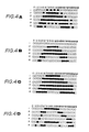
- a composite character dot pattern is a specific dot pattern as shown in FIG.4A. In this figure, lines following the sixth line are omitted for simplicity.
- a dot represented by "o” denotes a binary zero
- a dot represented by " ⁇ " denotes a binary one.
- FIG.4C shows a part of a character dot pattern which is normally stored in the conventional character generators and corresponds to the character which is the same as the character related to the specific character dot pattern shown in FIG.4A.
- FIG.4B shows a part of a dot pattern obtained by eliminating a dot pattern which forms a contour of the character dot pattern shown in FIG.4C. That is, the dot pattern shown in FIG.4B is the dot pattern of a center or inner portion of the character inside the contour.
- the dot pattern which forms the contour of the character dot pattern shown in FIG.4B is shown in FIG.4D. This pattern is hereafter referred to as a contour dot pattern.
- Various contour dot patterns can be formed without difficulties by arbitrarily extracting dots from the dot pattern shown in FIG.4C.
- a character dot pattern as shown in FIG.4A can be obtained from its contour dot pattern, for example.
- the composite character dot pattern shown in FIG.4A can be obtained by using the contour dot pattern shown in FIG.4D in the following manner.
- the contour dot pattern shown in FIG.4D is generated by performing the exclusive-OR operation between two adjacent dots in each line shown in FIG.4A. For example, in the first lines shown in FIGS.4A and 4D, the exclusive-OR operation is performed between the dots positioned at the sixth and seventh columns in the composite character dot pattern of FIG.4A, and as a result of the operation, a value is decided for the dot at the seventh column in the contour dot pattern of FIG.4D.
- values of the dots at the seventh column in the composite character dot pattern of FIG.4A can be obtained by use of the value of the dot at the sixth column in the dot pattern of FIG.4A and the value of the dot at the seventh column in the dot pattern shown in FIG.4D. Since the dot in the sixth column in FIG.4A has a value of 0, and the dot in the seventh column in FIG.4D has a value of 1, a value of the dot at the seventh column in FIG.4A is decided to be 1.
- This step for generating the dot data of the composite character dot pattern from the contour dot pattern is carried out starting with the dot positioned at the first column for each line.
- the dot at the first column of FIG.4D is initially processed.
- a value of the dot at the first column in FIG.4D is a value of the dot at the first column in FIG.4A as it is.
- the dot at the second column in FIG.4D is processed. Since the dot at the second column has a value of 0, a value of the dot at the second column is decided to be 0. In this manner, values of the dots at up to the sixth column in FIG.4A are decided to be 0.
- the value of the sixth column in FIG.4A which has already been obtained is referred to in addition to the value of the dot at the seventh column in FIG.4D. Since the dot at the sixth column in FIG.4A has a value of 0, and the dot at the seventh column in FIG.4D has a value of 1, a value of the dot at the seventh column in FIG.4A is decided to be 1. Subsequently, the dot at the eighth column in FIG.4D is processed. Since both the dot at the seventh column in FIG.4A and the dot at the eighth column in FIG.4D have values of 1, a value of the dot at the eighth column in FIG.4A is decided to be 0. In the above manner, the composite character dot pattern of FIG.4A can be obtained by using the contour dot pattern of FIG.4D.
- consecutive black dot data in each line of the contour dot pattern shown in FIG.4D are represented by an arrangment of consecutive dot data in the corresponding line of the composite character dot pattern shown in FIG.4A, in which black dot data are arranged for every other dot.
- consecutive white dot data inside the contour dot pattern are represented by an arrangment of consecutive black dot data in the corresponding line of the composite character dot patter shown in FIG.4A.
- a change from a white dot datum to a black dot datum in each line is represented as it is in the corresponding line of the composite character dot pattern shown in FIG.4A.
- White dot data outside the contour dot pattern are represented as they are.
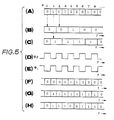
- a timing generator 27 supplies the character generator 26 with a raster address signal for designating the 32 lines in sequence through an address line 38. Thereby, data of the dots in the designated line of the composite character dot pattern corresponding to the character code are successively read out from the character generator 26 in a parallel form line by line. At this time, even-numbered bits are read out in parallel on a bus line 41, and odd-numbered bits are read out in parallel on a bus line 42.
- FIG.5A shows a portion of data which is simultaneously read out from the character generator 26 in which the even-numbered bits and the odd-numbered bits are arranged on the same axis in sequence for simplicity of the figure.
- the even-numbered bits and the odd-numbered bits are supplied to shift registers 29 and 28 through the bus lines 42 and 41, respectively.
- the shift registers 28 and 29 are provided with clock signals ⁇ 1 and ⁇ 2 having a phase difference of 180° which are generated by the timing generator 27 and are passed through through signal lines 39 and 40 respectively.
- the shift register 28 shifts each of the odd-numbered bits in parallel by respective predetermined times in synchronization with the clock signal ⁇ 1, as shown in FIG.5(C).
- a horizontal direction represents time.
- the odd-numbered bits are outputted per one bit in series starting with the smallest odd-numbered bit (# 1, in the illustrated example).
- Each of the outputted bits has a pulse width twice that of the original pulse width.
- the shift register 29 shifts each of the even-numbered bits in parallel by respective predetermined times in synchronization with the clock signal ⁇ 2, as shown in FIG.5(B).
- the even-numbered bits are outputted per one bit in series starting with the smallest even-numbered bit (# 0, in the illustrated example).
- Each of outputted bits has a pulse width twice that of the original pulse width.
- FIGS.5(B) and 5(C) adjacent even-numbered and odd-numbered bits shown in FIG.5(A) overlaps with each other on a time axis.
- the serial data from the shift registers 28 and 29 are supplied to an AND circuit 30, an OR circuit 31 and an exclusive OR circuit 32.
- Output signals of the AND circuit 30, OR circuit 31 and exclusive-OR circuit 32 shown in FIGS.5(F) through 5(H) are supplied to output terminals 33, 34 and 35, respectively.
- the output signal of the AND circuit 30 is a pattern display signal for displaying the pattern shown in FIG.4B, which is the same as the pattern stored in the memory 11 shown in FIG.2.
- the output signal is a pattern display signal for displaying the pattern shown in FIG.4C, which is the same as the pattern stored in the memory 10 shown in FIG.2.
- the output signal of the exclusive-OR circuit 32 is a contour highlighting display signal for displaying the pattern shown in FIG.4D, which is the same as the signal at the terminal 17 shown in FIG.2.
- the three different pattern display signals obtained by the present embodiment are generated from one pattern stored in the character generator 26.
- the conventional apparatus utilizes the two character generators each having the same memory capacity as that for the present embodiment. As a result, according to the embodiment, the memory capacity is half that for the conventional apparatus.
- different contour highlighting display signals can be easily obtained by varying the composite character dot patterns stored in the character generator 26. These results in an improved degree in the flexibility of the design of the display patterns.
- the output signals from the AND circuit 30, OR circuit 31 and exclusive-OR circuit 32 are supplied to a conventional signal processing circuit 60, respectively.
- the signal processing circuit 60 generates a video signal from the above signals.
- the luminance of the video signal may be controlled by the above signals. For example, the luminance of the video signal corresponding to the contour of the character is emphasized, compared to that for the inner portion thereof.
- the video signal is supplied to a cathode ray tube 70, so that the character is displayed on its picture plane in a state where the brightness of the contour is highlighted.
Abstract
Description
- The present invention generally relates to a pattern display signal generating apparatus, and in particular to a pattern display signal generating apparatus capable of generating a pattern display signal which enables a pattern to be displayed so that a contour of the character pattern is highlighted. The present invention further relates to a pattern display apparatus using the present pattern display signal generating apparatus.
- Conventionally, various display formats are used for producing a visual image of patterns of characters figures on a picture plane of a display unit such as television sets. Highlighting display of characters is one example of the display formats. For example, when highlighting the display of characters such as letters, numerals and symbols, the whole of a character is highly and uniformly intensified, or only a contour of the character is highly brightened. In the latter highlighting display, the contour of the character is visually emphasized compared to other portions thereof and is displayed.
- A display apparatus comprises a pattern display signal generating apparatus for generating a pattern display signal. The pattern display signal generating apparatus includes a character generator capable of generating dot patterns of characters. One dot pattern is arranged in a dot matrix of N lines and M columns. A dot pattern signal corresponding to one character is read out from the character generator line by line, and is supplied as a pattern display signal to a signal processing circuit. The signal processing circuit generates a video signal from the pattern display signal. The video signal is supplied to a display unit such as a cathode ray tube display unit, and the corresponding character is displayed on a display picture plane thereof.
- The conventional pattern display signal generating apparatus further includes an operation circuit for generating a specific pattern display signal which enables the highlighting display of the contour of the character (hereafter referred to as a contour highlighting display signal). The operation circuit generates the contour highlighting display signal corresponding to a dot pattern of only the contour of the character by using the dot pattern signal read out from the character generator. In this case, the contour of the dot pattern has a width of one dot in a direction of lines in the pattern (raster scan direction), for example.
- The contour highlighting display signal for forming the contour pattern having the width of one dot is generated by subjecting all the dots of an N × M dot matrix to the following processing. Referring to FIG.1 which shows a portion of the N × M dot matrix, when a dot positioned at the n'th line and the m'th column (hereafter represented as (n, m)) is processed, data of its neighboring dots, i.e., 8 dots represented by shaded squares are read out from the character generator in addition to the datum of the dot at the position (n, m). The operation circuit built in the pattern display signal generating apparatus performs a predetermined operation between the 9 dot data, and decides whether or not the dot at the position (n, m) is necessary to form the dot pattern of the contour. If a result of the operation is affirmative, the dot subjected to the operation is decided to be a dot for the contour.
- However, the above process for obtaining the dot pattern of the contour is very complex. In addition, the operation circuit which is designed specifically for implementing the above process cannot generate a different contour dot pattern having a width of two dots in the direction of the line for example. For this reason, a degree of flexibility in the display format of the highlighting contour is poor.
- In order to eliminate the above problems, a display pattern signal generating apparatus having a configuration shown in FIG.2 is proposed. Referring to FIG.2, a
memory 10 stores dot pattern data of various characters, and amemory 11 stores a dot pattern of a center (or inner) region of each character obtained by removing a dot pattern of a contour thereof. - The data which are simultaneously read out from the
memory shift registers shift registers output terminals shift registers OR circuit 13. A result of the exclusive-OR operation is a contour highlighting display signal related to the dot corresponding to the address ADDS. The contour highlighting display signal is supplied to anoutput terminal 17. In this manner, the contour highlighting display signal related to all the N × M dots is generated. - However, the configuration shown in FIG.2 must store two dot patterns associated with one character, and thus a large memory capacity is necessary.
- Accordingly, a general object of the present invention is to provide a novel and useful pattern display signal generating apparatus in which the disadvantages of the above conventional apparatus have been effectively eliminated.
- A more specific object of the present invention is to provide a pattern display signal generating apparatus of a simple configuration.
- Another object of the present invention is to provide a pattern display signal generating apparatus which can provide a higher degree of flexibility in the design of the highlighting display.
- Still another object of the present invention is to provide a pattern display signal generating apparatus capable of configuring a memory of a smaller capacity for storing dot patterns of characters.
- The above objects of the present invention can be achieved by a pattern display signal generating apparatus comprising a memory for storing predetermined pattern data and separately outputting even-numbered bits and odd-numbered bits of the pattern data in parallel when scanned, a timing generator for generating an address for scanning the memory and for generating first and second clock signals having a predetermined phase difference, a first shift register for shifting the odd-numbered bits and outputting the same in series in synchronization with the first clock signal, a second shift register for shifting the even-numbered bits and outputting the same in series in synchronization with the second clock signal, and a logical operation circuit for performing at least one predetermined logical operation between outputs of the first and second shift registers to generate a pattern display signal.
- A further object of the present invention is to provide a pattern display apparatus using the above pattern display signal generating apparatus.
- The above object of the present invention is achieved by a pattern display apparatus comprising a control circuit (signal processing unit) for designating a character code corresponding to a character pattern to be displayed, a pattern signal generating apparatus for generating pattern display signals corresponding to a pattern to be displayed, a signal processing circuit for subjecting the pattern display signals to predetermined signal processings and for generating a corresponding video signal, and a display unit for displaying a pattern corresponding to the video signal. The pattern generating signal generating apparatus comprises a display memory for storing the character code from the control circuit, a memory (character generator) for storing predetermined pattern data and separately outputting even-numbered bits and odd-numbered bits of the pattern data in parallel when a pattern data designated by the character code from the display memory is scanned, a timing generator for generating an address for scanning the memory and for generating first and second clock signals having a predetermined phase difference, a first shift register for shifting the odd-numbered bits and outputting the same in series in synchronization with the first clock signal, a second shift register for shifting the even-numbered bits and outputting the same in series in synchronization with the second clock signal, and a logical operation circuit for performing a plurality of predetermined logical operations between outputs of the first and second shift registers to generate the pattern display signals to be supplied to the signal processing circuit.
- Other objects, features and advantages of the present invention will become apparent from the following detailed description when read in conjunction with the accompanying drawings.
-
- FIG.1 is a view for explaining an example of the conventional apparatus for generating a display signal for displaying a highlighting contour of a character;
- FIG.2 is a block diagram of an another example of the conventional apparatus for generating a display signal for displaying a highlighting contour of a character;
- FIG.3 is a block diagram of a preferred embodiment of the present invention which is a part constituting a visual display apparatus;
- FIG.4A is a view for showing a part of a character dot pattern stored in a character generator shown in FIG.3;
- FIG.4B through 4D are views for showing parts of character dot patterns which can be generated by the configuration shown in FIG.3; and
- FIGS.5(A) through 5(H) are views for explaining digital signals at different parts in the configuration shown in FIG.3.
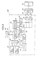
- Referring to FIG.3, a
reference numeral 100 denotes an preferred embodiment of the present invention. A central processing unit (hereafter simply referred to as a CPU) 50 provides adisplay memory 24 with a character code corresponding to a character to be displayed through aterminal 25. Awrite address counter 20 generates a write address for thedisplay memory 24, and aread address counter 21 generates a read address for thedisplay memory 24. The write address and the read address are supplied to aselector 22. Acontroller 23 generates a read/write switching signal (hereafter simply referred to as R/W switching signal), and supplies the same to theselector 22 through asignal line 36. When theCPU 50 outputs the character code to thedisplay memory 24, thecontroller 23 provides theselector 22 with the R/W switching signal having a signal state which designates the selection of the write address generated by thewrite address counter 20. At this time, thedisplay memory 24 is maintained in a write mode which is designated by a read/write signal which is generated by thecontroller 23 and is passed through asignal line 37. - The
display memory 24 is used to temporarily store character codes, each of which indicates a corresponding character. When reading out the desired character code from thedisplay memory 24, it is kept in a read mode designated by the read/write signal from thecontroller 23. The character code in thedisplay memory 24 is read out therefrom and is supplied to acharacter generator 26. At this time, thecontroller 23 generates the R/W switching signal having a state which designates the selection of the read address generated by theread address counter 21. - The
character generator 26 is a memory in which composite character dot patterns each of which corresponds to respective character codes. Each of the composite character patterns is composed of 32 (lines) × 24 (columns) dots, for example. A composite character dot pattern is a specific dot pattern as shown in FIG.4A. In this figure, lines following the sixth line are omitted for simplicity. A dot represented by "o" denotes a binary zero, and a dot represented by "●" denotes a binary one. - Character dot patterns stored in the
character generator 26 are different from those stored in the conventional character generators. FIG.4C shows a part of a character dot pattern which is normally stored in the conventional character generators and corresponds to the character which is the same as the character related to the specific character dot pattern shown in FIG.4A. FIG.4B shows a part of a dot pattern obtained by eliminating a dot pattern which forms a contour of the character dot pattern shown in FIG.4C. That is, the dot pattern shown in FIG.4B is the dot pattern of a center or inner portion of the character inside the contour. The dot pattern which forms the contour of the character dot pattern shown in FIG.4B is shown in FIG.4D. This pattern is hereafter referred to as a contour dot pattern. Various contour dot patterns can be formed without difficulties by arbitrarily extracting dots from the dot pattern shown in FIG.4C. - A character dot pattern as shown in FIG.4A can be obtained from its contour dot pattern, for example. By way of example, the composite character dot pattern shown in FIG.4A can be obtained by using the contour dot pattern shown in FIG.4D in the following manner. As will be described in detail later, the contour dot pattern shown in FIG.4D is generated by performing the exclusive-OR operation between two adjacent dots in each line shown in FIG.4A. For example, in the first lines shown in FIGS.4A and 4D, the exclusive-OR operation is performed between the dots positioned at the sixth and seventh columns in the composite character dot pattern of FIG.4A, and as a result of the operation, a value is decided for the dot at the seventh column in the contour dot pattern of FIG.4D. Therefore, values of the dots at the seventh column in the composite character dot pattern of FIG.4A can be obtained by use of the value of the dot at the sixth column in the dot pattern of FIG.4A and the value of the dot at the seventh column in the dot pattern shown in FIG.4D. Since the dot in the sixth column in FIG.4A has a value of 0, and the dot in the seventh column in FIG.4D has a value of 1, a value of the dot at the seventh column in FIG.4A is decided to be 1. This step for generating the dot data of the composite character dot pattern from the contour dot pattern is carried out starting with the dot positioned at the first column for each line.
- For example, when deciding values of the dots in the first line of FIG.4A, the dot at the first column of FIG.4D is initially processed. A value of the dot at the first column in FIG.4D is a value of the dot at the first column in FIG.4A as it is. Next, the dot at the second column in FIG.4D is processed. Since the dot at the second column has a value of 0, a value of the dot at the second column is decided to be 0. In this manner, values of the dots at up to the sixth column in FIG.4A are decided to be 0. Thereafter, when the dot at the seventh column in FIG.4D is processed, the value of the sixth column in FIG.4A which has already been obtained is referred to in addition to the value of the dot at the seventh column in FIG.4D. Since the dot at the sixth column in FIG.4A has a value of 0, and the dot at the seventh column in FIG.4D has a value of 1, a value of the dot at the seventh column in FIG.4A is decided to be 1. Subsequently, the dot at the eighth column in FIG.4D is processed. Since both the dot at the seventh column in FIG.4A and the dot at the eighth column in FIG.4D have values of 1, a value of the dot at the eighth column in FIG.4A is decided to be 0. In the above manner, the composite character dot pattern of FIG.4A can be obtained by using the contour dot pattern of FIG.4D.
- The above process may be summarized as follows. Firstly, consecutive black dot data in each line of the contour dot pattern shown in FIG.4D are represented by an arrangment of consecutive dot data in the corresponding line of the composite character dot pattern shown in FIG.4A, in which black dot data are arranged for every other dot. Secondly, consecutive white dot data inside the contour dot pattern are represented by an arrangment of consecutive black dot data in the corresponding line of the composite character dot patter shown in FIG.4A. Thirdly, a change from a white dot datum to a black dot datum in each line is represented as it is in the corresponding line of the composite character dot pattern shown in FIG.4A. White dot data outside the contour dot pattern are represented as they are.
- Returning to FIG.3, a
timing generator 27 supplies thecharacter generator 26 with a raster address signal for designating the 32 lines in sequence through anaddress line 38. Thereby, data of the dots in the designated line of the composite character dot pattern corresponding to the character code are successively read out from thecharacter generator 26 in a parallel form line by line. At this time, even-numbered bits are read out in parallel on abus line 41, and odd-numbered bits are read out in parallel on abus line 42. - FIG.5A shows a portion of data which is simultaneously read out from the
character generator 26 in which the even-numbered bits and the odd-numbered bits are arranged on the same axis in sequence for simplicity of the figure. The even-numbered bits and the odd-numbered bits are supplied to shiftregisters bus lines timing generator 27 and are passed through throughsignal lines shift register 28 shifts each of the odd-numbered bits in parallel by respective predetermined times in synchronization with the clock signal ø₁, as shown in FIG.5(C). In FIG.5(C), a horizontal direction represents time. Then, the odd-numbered bits are outputted per one bit in series starting with the smallest odd-numbered bit (# 1, in the illustrated example). Each of the outputted bits has a pulse width twice that of the original pulse width. Likewise, theshift register 29 shifts each of the even-numbered bits in parallel by respective predetermined times in synchronization with the clock signal ø₂, as shown in FIG.5(B). Then, the even-numbered bits are outputted per one bit in series starting with the smallest even-numbered bit (# 0, in the illustrated example). Each of outputted bits has a pulse width twice that of the original pulse width. - As shown in FIGS.5(B) and 5(C), adjacent even-numbered and odd-numbered bits shown in FIG.5(A) overlaps with each other on a time axis. The serial data from the shift registers 28 and 29 are supplied to an AND
circuit 30, an ORcircuit 31 and an exclusive ORcircuit 32. Output signals of the ANDcircuit 30, ORcircuit 31 and exclusive-OR circuit 32 shown in FIGS.5(F) through 5(H) are supplied tooutput terminals circuit 30 is a pattern display signal for displaying the pattern shown in FIG.4B, which is the same as the pattern stored in thememory 11 shown in FIG.2. The output signal is a pattern display signal for displaying the pattern shown in FIG.4C, which is the same as the pattern stored in thememory 10 shown in FIG.2. The output signal of the exclusive-OR circuit 32 is a contour highlighting display signal for displaying the pattern shown in FIG.4D, which is the same as the signal at the terminal 17 shown in FIG.2. It will be appreciated that the three different pattern display signals obtained by the present embodiment are generated from one pattern stored in thecharacter generator 26. On the other hand, the conventional apparatus utilizes the two character generators each having the same memory capacity as that for the present embodiment. As a result, according to the embodiment, the memory capacity is half that for the conventional apparatus. In addition to the above advantage, different contour highlighting display signals can be easily obtained by varying the composite character dot patterns stored in thecharacter generator 26. These results in an improved degree in the flexibility of the design of the display patterns. - The output signals from the AND
circuit 30, ORcircuit 31 and exclusive-OR circuit 32 are supplied to a conventionalsignal processing circuit 60, respectively. Thesignal processing circuit 60 generates a video signal from the above signals. At this time, the luminance of the video signal may be controlled by the above signals. For example, the luminance of the video signal corresponding to the contour of the character is emphasized, compared to that for the inner portion thereof. The video signal is supplied to acathode ray tube 70, so that the character is displayed on its picture plane in a state where the brightness of the contour is highlighted. - The present invention is not limited to the above embodiment, but various variations and modifications may be made without departing from the scope of the present invention.
Claims (11)
Applications Claiming Priority (2)
| Application Number | Priority Date | Filing Date | Title |
|---|---|---|---|
| JP62070730A JPH068990B2 (en) | 1987-03-25 | 1987-03-25 | Pattern display signal generator |
| JP70730/87 | 1987-03-25 |
Publications (3)
| Publication Number | Publication Date |
|---|---|
| EP0284326A2 true EP0284326A2 (en) | 1988-09-28 |
| EP0284326A3 EP0284326A3 (en) | 1990-01-10 |
| EP0284326B1 EP0284326B1 (en) | 1993-02-03 |
Family
ID=13439943
Family Applications (1)
| Application Number | Title | Priority Date | Filing Date |
|---|---|---|---|
| EP88302453A Expired - Lifetime EP0284326B1 (en) | 1987-03-25 | 1988-03-21 | Pattern display signal generating apparatus and display apparatus using the same |
Country Status (5)
| Country | Link |
|---|---|
| US (1) | US5003304A (en) |
| EP (1) | EP0284326B1 (en) |
| JP (1) | JPH068990B2 (en) |
| KR (1) | KR910005364B1 (en) |
| DE (1) | DE3877994T2 (en) |
Cited By (2)
| Publication number | Priority date | Publication date | Assignee | Title |
|---|---|---|---|---|
| EP0375219A2 (en) * | 1988-12-21 | 1990-06-27 | Fujitsu Limited | Method and apparatus for forming outline character |
| EP0542316A2 (en) * | 1991-11-15 | 1993-05-19 | Seiko Epson Corporation | Bit map data generation apparatus |
Families Citing this family (5)
| Publication number | Priority date | Publication date | Assignee | Title |
|---|---|---|---|---|
| KR920010811B1 (en) * | 1990-05-10 | 1992-12-17 | 주식회사 금성사 | Tv teletext apparatus |
| FR2664999B1 (en) * | 1990-07-23 | 1992-09-18 | Bull Sa | DATA OUTPUT INPUT DEVICE FOR DISPLAYING INFORMATION AND METHOD USED BY SUCH A DEVICE. |
| JP2726951B2 (en) * | 1990-08-24 | 1998-03-11 | 富士ゼロックス株式会社 | Character / graphic drawing device |
| US5909519A (en) * | 1996-05-21 | 1999-06-01 | Hewlett-Packard Company | Method for printing pseudo-bold characters at arbitrary orientations, scaling, and resolutions |
| US7551475B2 (en) | 2006-04-03 | 2009-06-23 | International Business Machines Corporation | Data shifting through scan registers |
Citations (2)
| Publication number | Priority date | Publication date | Assignee | Title |
|---|---|---|---|---|
| EP0076082A2 (en) * | 1981-09-21 | 1983-04-06 | Nec Corporation | Display processing apparatus |
| EP0128291A2 (en) * | 1983-05-11 | 1984-12-19 | International Business Machines Corporation | Independent image and annotation overlay with highlighting of overlay conflicts |
Family Cites Families (3)
| Publication number | Priority date | Publication date | Assignee | Title |
|---|---|---|---|---|
| JPS57187257A (en) * | 1981-05-15 | 1982-11-17 | Fuji Xerox Co Ltd | Printing system |
| US4408198A (en) * | 1981-09-14 | 1983-10-04 | Shintron Company, Inc. | Video character generator |
| US4613856A (en) * | 1983-04-04 | 1986-09-23 | Tektronix, Inc. | Character and video mode control circuit |
-
1987
- 1987-03-25 JP JP62070730A patent/JPH068990B2/en not_active Expired - Fee Related
-
1988
- 1988-03-21 DE DE8888302453T patent/DE3877994T2/en not_active Expired - Fee Related
- 1988-03-21 EP EP88302453A patent/EP0284326B1/en not_active Expired - Lifetime
- 1988-03-25 KR KR8803231A patent/KR910005364B1/en not_active IP Right Cessation
-
1990
- 1990-05-23 US US07/526,948 patent/US5003304A/en not_active Expired - Lifetime
Patent Citations (2)
| Publication number | Priority date | Publication date | Assignee | Title |
|---|---|---|---|---|
| EP0076082A2 (en) * | 1981-09-21 | 1983-04-06 | Nec Corporation | Display processing apparatus |
| EP0128291A2 (en) * | 1983-05-11 | 1984-12-19 | International Business Machines Corporation | Independent image and annotation overlay with highlighting of overlay conflicts |
Cited By (6)
| Publication number | Priority date | Publication date | Assignee | Title |
|---|---|---|---|---|
| EP0375219A2 (en) * | 1988-12-21 | 1990-06-27 | Fujitsu Limited | Method and apparatus for forming outline character |
| EP0375219A3 (en) * | 1988-12-21 | 1990-08-08 | Fujitsu Limited | Method and apparatus for forming outline character |
| US5099230A (en) * | 1988-12-21 | 1992-03-24 | Fujitsu Limited | Method of and apparatus for forming outline character |
| EP0542316A2 (en) * | 1991-11-15 | 1993-05-19 | Seiko Epson Corporation | Bit map data generation apparatus |
| EP0542316A3 (en) * | 1991-11-15 | 1994-01-05 | Seiko Epson Corp | |
| US5457774A (en) * | 1991-11-15 | 1995-10-10 | Seiko Epson Corporation | Bit map data generation apparatus |
Also Published As
| Publication number | Publication date |
|---|---|
| US5003304A (en) | 1991-03-26 |
| KR910005364B1 (en) | 1991-07-29 |
| KR880011696A (en) | 1988-10-29 |
| JPS63236088A (en) | 1988-09-30 |
| EP0284326B1 (en) | 1993-02-03 |
| DE3877994D1 (en) | 1993-03-18 |
| DE3877994T2 (en) | 1993-05-27 |
| JPH068990B2 (en) | 1994-02-02 |
| EP0284326A3 (en) | 1990-01-10 |
Similar Documents
| Publication | Publication Date | Title |
|---|---|---|
| EP0199989B1 (en) | Method and system for image processing | |
| US4439762A (en) | Graphics memory expansion system | |
| US4246578A (en) | Pattern generation display system | |
| US4630039A (en) | Display processing apparatus | |
| EP0139932A2 (en) | Apparatus for generating the display of a cursor | |
| US4095216A (en) | Method and apparatus for displaying alphanumeric data | |
| US4409591A (en) | Variable size character generator | |
| EP0284326B1 (en) | Pattern display signal generating apparatus and display apparatus using the same | |
| US5068651A (en) | Image display apparatus | |
| US4345243A (en) | Apparatus for generating signals for producing a display of characters | |
| US5606656A (en) | Image data processing unit for forming a plurality of identical images in a single output image area | |
| EP0400990A2 (en) | Apparatus for superimposing character patterns in accordance with dot-matrix on video signals | |
| JPH10233915A (en) | Image processor | |
| KR100266930B1 (en) | Method of drawing figure such as polygon and display control device | |
| EP0510182B1 (en) | Image scaling for thermal printers and the like | |
| EP0242139B1 (en) | Display controller | |
| JP2570755B2 (en) | Pattern generator | |
| JP2732172B2 (en) | Video display device | |
| SU1037329A1 (en) | Device for displaying data on cathode-ray tube screen | |
| JP2647073B2 (en) | Graphic display device | |
| JP2987983B2 (en) | Character display device | |
| JPH05313643A (en) | Character attribute synthesizing device of character display device | |
| JPS5854395B2 (en) | Character pattern generation method | |
| JPH0612048A (en) | Picture display device | |
| JPH0614267A (en) | Display device |
Legal Events
| Date | Code | Title | Description |
|---|---|---|---|
| PUAI | Public reference made under article 153(3) epc to a published international application that has entered the european phase |
Free format text: ORIGINAL CODE: 0009012 |
|
| AK | Designated contracting states |
Kind code of ref document: A2 Designated state(s): DE FR GB |
|
| PUAL | Search report despatched |
Free format text: ORIGINAL CODE: 0009013 |
|
| AK | Designated contracting states |
Kind code of ref document: A3 Designated state(s): DE FR GB |
|
| 17P | Request for examination filed |
Effective date: 19900119 |
|
| 17Q | First examination report despatched |
Effective date: 19911113 |
|
| GRAA | (expected) grant |
Free format text: ORIGINAL CODE: 0009210 |
|
| AK | Designated contracting states |
Kind code of ref document: B1 Designated state(s): DE FR GB |
|
| RAP2 | Party data changed (patent owner data changed or rights of a patent transferred) |
Owner name: FUJITSU DEVICES INC Owner name: FUJITSU LIMITED |
|
| REF | Corresponds to: |
Ref document number: 3877994 Country of ref document: DE Date of ref document: 19930318 |
|
| ET | Fr: translation filed | ||
| PLBE | No opposition filed within time limit |
Free format text: ORIGINAL CODE: 0009261 |
|
| STAA | Information on the status of an ep patent application or granted ep patent |
Free format text: STATUS: NO OPPOSITION FILED WITHIN TIME LIMIT |
|
| 26N | No opposition filed | ||
| PGFP | Annual fee paid to national office [announced via postgrant information from national office to epo] |
Ref country code: GB Payment date: 19960312 Year of fee payment: 9 |
|
| PGFP | Annual fee paid to national office [announced via postgrant information from national office to epo] |
Ref country code: FR Payment date: 19960315 Year of fee payment: 9 |
|
| PGFP | Annual fee paid to national office [announced via postgrant information from national office to epo] |
Ref country code: DE Payment date: 19960328 Year of fee payment: 9 |
|
| PG25 | Lapsed in a contracting state [announced via postgrant information from national office to epo] |
Ref country code: GB Effective date: 19970321 |
|
| GBPC | Gb: european patent ceased through non-payment of renewal fee |
Effective date: 19970321 |
|
| PG25 | Lapsed in a contracting state [announced via postgrant information from national office to epo] |
Ref country code: FR Free format text: LAPSE BECAUSE OF NON-PAYMENT OF DUE FEES Effective date: 19971128 |
|
| PG25 | Lapsed in a contracting state [announced via postgrant information from national office to epo] |
Ref country code: DE Effective date: 19971202 |
|
| REG | Reference to a national code |
Ref country code: FR Ref legal event code: ST |