EP0281676B1 - Radiation detector with an ionizable gas atop an integrated circuit - Google Patents
Radiation detector with an ionizable gas atop an integrated circuit Download PDFInfo
- Publication number
- EP0281676B1 EP0281676B1 EP87118193A EP87118193A EP0281676B1 EP 0281676 B1 EP0281676 B1 EP 0281676B1 EP 87118193 A EP87118193 A EP 87118193A EP 87118193 A EP87118193 A EP 87118193A EP 0281676 B1 EP0281676 B1 EP 0281676B1
- Authority
- EP
- European Patent Office
- Prior art keywords
- radiation
- gas
- detector
- radiation detector
- collecting electrode
- Prior art date
- Legal status (The legal status is an assumption and is not a legal conclusion. Google has not performed a legal analysis and makes no representation as to the accuracy of the status listed.)
- Expired - Lifetime
Links
- 230000005855 radiation Effects 0.000 title claims description 161
- 238000001514 detection method Methods 0.000 claims abstract description 28
- 230000003139 buffering effect Effects 0.000 claims abstract 3
- 150000002500 ions Chemical class 0.000 claims description 90
- 230000005684 electric field Effects 0.000 claims description 51
- 230000008878 coupling Effects 0.000 claims description 10
- 238000010168 coupling process Methods 0.000 claims description 10
- 238000005859 coupling reaction Methods 0.000 claims description 10
- 230000001419 dependent effect Effects 0.000 claims description 10
- 230000004907 flux Effects 0.000 claims description 8
- 238000005259 measurement Methods 0.000 claims description 8
- 239000000463 material Substances 0.000 claims description 7
- 238000012544 monitoring process Methods 0.000 claims description 5
- 239000007789 gas Substances 0.000 description 70
- 230000015654 memory Effects 0.000 description 25
- 239000004033 plastic Substances 0.000 description 25
- 229920003023 plastic Polymers 0.000 description 25
- 238000010586 diagram Methods 0.000 description 23
- 239000003990 capacitor Substances 0.000 description 15
- 238000004891 communication Methods 0.000 description 15
- 239000000758 substrate Substances 0.000 description 14
- 210000001519 tissue Anatomy 0.000 description 10
- 239000000872 buffer Substances 0.000 description 9
- 238000000034 method Methods 0.000 description 9
- 230000008859 change Effects 0.000 description 8
- 238000012546 transfer Methods 0.000 description 6
- 230000006870 function Effects 0.000 description 5
- 230000004044 response Effects 0.000 description 5
- 102000012677 DET1 Human genes 0.000 description 4
- 101150113651 DET1 gene Proteins 0.000 description 4
- 238000011109 contamination Methods 0.000 description 4
- 230000006798 recombination Effects 0.000 description 4
- 238000005215 recombination Methods 0.000 description 4
- 230000035945 sensitivity Effects 0.000 description 4
- 230000033228 biological regulation Effects 0.000 description 3
- 229910052799 carbon Inorganic materials 0.000 description 3
- 230000003247 decreasing effect Effects 0.000 description 3
- 230000007613 environmental effect Effects 0.000 description 3
- 101100484492 Arabidopsis thaliana VHA-C gene Proteins 0.000 description 2
- XKRFYHLGVUSROY-UHFFFAOYSA-N Argon Chemical compound [Ar] XKRFYHLGVUSROY-UHFFFAOYSA-N 0.000 description 2
- IJGRMHOSHXDMSA-UHFFFAOYSA-N Atomic nitrogen Chemical compound N#N IJGRMHOSHXDMSA-UHFFFAOYSA-N 0.000 description 2
- OKTJSMMVPCPJKN-UHFFFAOYSA-N Carbon Chemical compound [C] OKTJSMMVPCPJKN-UHFFFAOYSA-N 0.000 description 2
- RYGMFSIKBFXOCR-UHFFFAOYSA-N Copper Chemical compound [Cu] RYGMFSIKBFXOCR-UHFFFAOYSA-N 0.000 description 2
- 101150066284 DET2 gene Proteins 0.000 description 2
- VYPSYNLAJGMNEJ-UHFFFAOYSA-N Silicium dioxide Chemical compound O=[Si]=O VYPSYNLAJGMNEJ-UHFFFAOYSA-N 0.000 description 2
- 229910000831 Steel Inorganic materials 0.000 description 2
- 230000004888 barrier function Effects 0.000 description 2
- 230000000295 complement effect Effects 0.000 description 2
- 229910052802 copper Inorganic materials 0.000 description 2
- 239000010949 copper Substances 0.000 description 2
- 230000009977 dual effect Effects 0.000 description 2
- 230000000694 effects Effects 0.000 description 2
- PCHJSUWPFVWCPO-UHFFFAOYSA-N gold Chemical compound [Au] PCHJSUWPFVWCPO-UHFFFAOYSA-N 0.000 description 2
- 229910052737 gold Inorganic materials 0.000 description 2
- 239000010931 gold Substances 0.000 description 2
- 230000005865 ionizing radiation Effects 0.000 description 2
- 238000002955 isolation Methods 0.000 description 2
- 238000004519 manufacturing process Methods 0.000 description 2
- 229910052757 nitrogen Inorganic materials 0.000 description 2
- 230000036961 partial effect Effects 0.000 description 2
- 239000002245 particle Substances 0.000 description 2
- 230000008569 process Effects 0.000 description 2
- 230000001681 protective effect Effects 0.000 description 2
- 239000010959 steel Substances 0.000 description 2
- 230000001960 triggered effect Effects 0.000 description 2
- 239000002699 waste material Substances 0.000 description 2
- 208000032953 Device battery issue Diseases 0.000 description 1
- 239000004593 Epoxy Substances 0.000 description 1
- 101710144121 Non-structural protein 5 Proteins 0.000 description 1
- 239000004698 Polyethylene Substances 0.000 description 1
- 231100000987 absorbed dose Toxicity 0.000 description 1
- 238000010521 absorption reaction Methods 0.000 description 1
- 238000009825 accumulation Methods 0.000 description 1
- 239000000853 adhesive Substances 0.000 description 1
- 230000001070 adhesive effect Effects 0.000 description 1
- 239000003570 air Substances 0.000 description 1
- 239000004411 aluminium Substances 0.000 description 1
- 229910052782 aluminium Inorganic materials 0.000 description 1
- 229910052786 argon Inorganic materials 0.000 description 1
- 230000005540 biological transmission Effects 0.000 description 1
- WUKWITHWXAAZEY-UHFFFAOYSA-L calcium difluoride Chemical compound [F-].[F-].[Ca+2] WUKWITHWXAAZEY-UHFFFAOYSA-L 0.000 description 1
- 229910001634 calcium fluoride Inorganic materials 0.000 description 1
- 238000004364 calculation method Methods 0.000 description 1
- 239000006229 carbon black Substances 0.000 description 1
- 230000001143 conditioned effect Effects 0.000 description 1
- 238000010276 construction Methods 0.000 description 1
- 125000004122 cyclic group Chemical group 0.000 description 1
- 230000007547 defect Effects 0.000 description 1
- 238000011161 development Methods 0.000 description 1
- 238000009792 diffusion process Methods 0.000 description 1
- 239000012777 electrically insulating material Substances 0.000 description 1
- 239000007772 electrode material Substances 0.000 description 1
- 238000005516 engineering process Methods 0.000 description 1
- 239000013056 hazardous product Substances 0.000 description 1
- 229910052739 hydrogen Inorganic materials 0.000 description 1
- 238000002347 injection Methods 0.000 description 1
- 239000007924 injection Substances 0.000 description 1
- 238000009413 insulation Methods 0.000 description 1
- 230000000670 limiting effect Effects 0.000 description 1
- 239000000203 mixture Substances 0.000 description 1
- 238000012986 modification Methods 0.000 description 1
- 230000004048 modification Effects 0.000 description 1
- 210000003205 muscle Anatomy 0.000 description 1
- QJGQUHMNIGDVPM-UHFFFAOYSA-N nitrogen group Chemical group [N] QJGQUHMNIGDVPM-UHFFFAOYSA-N 0.000 description 1
- 230000003287 optical effect Effects 0.000 description 1
- 229910052760 oxygen Inorganic materials 0.000 description 1
- 238000002161 passivation Methods 0.000 description 1
- 230000000737 periodic effect Effects 0.000 description 1
- -1 polyethylene Polymers 0.000 description 1
- 229920000573 polyethylene Polymers 0.000 description 1
- 238000012545 processing Methods 0.000 description 1
- 238000000275 quality assurance Methods 0.000 description 1
- 230000002285 radioactive effect Effects 0.000 description 1
- 229910052704 radon Inorganic materials 0.000 description 1
- SYUHGPGVQRZVTB-UHFFFAOYSA-N radon atom Chemical compound [Rn] SYUHGPGVQRZVTB-UHFFFAOYSA-N 0.000 description 1
- 230000002829 reductive effect Effects 0.000 description 1
- 230000002441 reversible effect Effects 0.000 description 1
- 238000000926 separation method Methods 0.000 description 1
- 235000012239 silicon dioxide Nutrition 0.000 description 1
- 239000000377 silicon dioxide Substances 0.000 description 1
- 239000007787 solid Substances 0.000 description 1
- 239000011343 solid material Substances 0.000 description 1
- 239000000126 substance Substances 0.000 description 1
- 230000001360 synchronised effect Effects 0.000 description 1
- 230000000007 visual effect Effects 0.000 description 1
- XLYOFNOQVPJJNP-UHFFFAOYSA-N water Substances O XLYOFNOQVPJJNP-UHFFFAOYSA-N 0.000 description 1
Images





Classifications
-
- H—ELECTRICITY
- H01—ELECTRIC ELEMENTS
- H01J—ELECTRIC DISCHARGE TUBES OR DISCHARGE LAMPS
- H01J47/00—Tubes for determining the presence, intensity, density or energy of radiation or particles
- H01J47/02—Ionisation chambers
-
- G—PHYSICS
- G01—MEASURING; TESTING
- G01T—MEASUREMENT OF NUCLEAR OR X-RADIATION
- G01T1/00—Measuring X-radiation, gamma radiation, corpuscular radiation, or cosmic radiation
- G01T1/16—Measuring radiation intensity
- G01T1/185—Measuring radiation intensity with ionisation chamber arrangements
-
- G—PHYSICS
- G01—MEASURING; TESTING
- G01T—MEASUREMENT OF NUCLEAR OR X-RADIATION
- G01T7/00—Details of radiation-measuring instruments
- G01T7/12—Provision for actuation of an alarm
- G01T7/125—Alarm- or controlling circuits using ionisation chambers, proportional counters or Geiger-Mueller tubes, also functioning as UV detectors
Definitions
- the invention refers to a radiation detector means for measuring radiation comprising the features according to the preamble of claim 1.
- a radiation detector means of the aforementioned art is known from IEEE Transactions on Nuclear Science (Vol. NS26, No. 4, August 1979, pages 4596 ff.), wherein the radiation detector means is named multichannel electrometer system.
- This known electrometer comprises an array of ionization chambers which are closely spaced by about 2 cm.
- An essential disadvantage of this electrometer is the separation of the different ionization chamber detectors and their corresponding electrometer circuitries. Therefore, cables etc. are necessary for the connection of the ionization chambers and the electrometer circuitries. Additionally, each electrometer is housed in a cast-aluminium box. These disadvantages therefore do not allow a high accuracy in measuring the corresponding radiation.
- Ionizing radiation presents a direct hazard to people; therefore, the measurement of radiation in environmental settings is important.
- the type of radiation monitor or detector used to measure the radiation depends upon the type of radiation, e.g., beta, alpha or X-ray and the environmental setting, e.g., an environmentally isolated laboratory, an open mine, a waste dump holding potentially hazardous material.
- the laboratory most likely requires a monitoring system with a continuous display and singular or multiple radiation detectors; the mine requires a moderately sensitive portable area detector; and the waste dump a relatively sensitive, directional detector.
- the portable monitor consists of a Geiger-Muller tube (GM tube) with an event counter which records the number of ionizing events. There is a readout display and an audio alarm.
- GM tube Geiger-Muller tube
- the problem with the GM tube is that its response is not linear with the energy of the radiation so its accuracy varies with radiation energy, although it is useful for warning.
- the radiation detector means includes at least one radiation detection sub-assembly and a detector control means and interface unit.
- Each subassembly includes a hemispheric bubble of electrically conductive tissue equivalent plastic which defines a volume of gas within the bubble. The gas is adapted to be ionized by radiation incident thereon.
- An integrated circuit (herein IC) is mounted below the volume of gas.
- a collecting electrode on the surface of the IC, is in direct contact with the gas and collects ions resulting from the ionization of the gas by the radiation.
- the IC includes an amplifier that incorporates the collecting electrode.
- the detector control and interface unit conditions the signal from the amplifier and buffers that signal.
- the unit includes a sensing amplifier that acts as a comparator, and a counter which is used to control the detection subassembly.
- the collecting electrode is a control gate for an amplifying transistor in the incorporated amplifier. An electric field within the volume of gas moves ions of one polarity toward the collecting electrode.
- the control gate/collecting electrode is biased to a predetermined level which changes due to the collected ions and therefore the output of the amplifying transistor is a signal representative of the amount of ions collected.
- the signal is applied to the interface and passed to the sense amplifier. When the conditioned signal passes a predetermined threshold, the counter is triggered and is incremented.
- Triggering the counter also commands a circuit to clear or restore a predetermined bias level to the control gate (the collecting electrode) of the amplifying transistor.
- the interface may additionally include a dose and dose rate computer, a memory and a communications section.
- the voltage level (bias) of the collecting electrode is switched from a high and to a low level or vice versa upon receipt of a triggering pulse, thereby eliminating the need to electrically connect a voltage source to the collecting electrode to clear the accumulated charge.
- Electrodes can be used on the surface of the IC and configured either as collecting electrodes or biasing electrodes. In the latter configuration, the flux lines of the electric field extend between the biasing electrodes and the collecting electrodes. Otherwise, the electric field extends between the collecting electrodes and the interior surface of the conductive plastic defining the bubble of gas.
- Another embodiment of the present invention utilizes several volumes of gas disposed above a single IC.
- the IC has a plurality of collecting electrodes in direct contact with each volume of gas.
- one volume of gas is displaced from atop the IC by a small distance.
- the IC and the corresponding collecting electrode in the offset volume of gas are mounted on the substrate. The electrode is electrically coupled to the amplifier in the IC.
- the radiation detector may be used in a calibration and display device. Further, a plurality of radiation detectors can be configured as an area network.
- This invention relates generally to a radiation detector and particularly to a radiation detector with a volume of ionizable gas atop a solid-state integrated circuit.
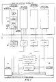
- FIG. 1 illustrates a functional block diagram of the radiation detector.
- Radiation detector 10 includes two general sections, a radiation detection assembly 12 and a detector control and interface unit 14.
- Radiation detection assembly 12 includes radiation detection subassemblies 1, 2...n-1, n. Each detection subassembly includes similar items as those depicted in detection subassembly 1.
- An ion chamber 16 holds a volume of ionizable gas atop an integrated circuit having a collecting or sensing electrode in direct contact with the gas.
- a field generator 18 develops an electrical field within the volume of gas and moves the ions in the gas created by radiation.
- the signal from the collecting electrode is applied to amplifier 20 and is subsequently applied to a leakage compensation and discharge controller1 22 in detector control and interface unit 14.
- the detection subassembly 1 may include leakage compensation circuit A 24. Since the collecting electrode attracts ions in the gas due to the bias placed thereon, the subassembly includes charge removal device 26 that is coupled to the input of amplifier 20 and the input of field generator 18. The specific circuitry for charge removal device 26 and its operation is described later with respect to Figures 15 through 22.
- Leakage compensation and discharge circuit1 22 controls charge removal device 26.
- Leakage compensation and discharge unit1 22 is coupled to dose and dose rate calculator and controller 30, memories 32, human interface 34 and electronic interface 36.
- the dose and dose rate calculator and controller generally determines the total amount of radiation the radiation detector has been subjected to as well as the rate at which the detector detects the radiation. These items are stored as radiation count data in the memories 32.
- the radiation detector may be embodied as CMOS integrated circuit elements to reduce power requirements and hence reduce the size of a power supply.
- the power can be internal to the detector and can be a battery; the power supply and the battery are not shown in Figure 1.
- Various detection subassemblies and associated circuits in the detector control can be embodied as a plurality of integrated circuits (ICs). These ICs can be coupled to a microcomputer on a chip that functions as dose and dose rate calculator and controller 30, memories 32, human interface 34 and electronic interface 36. In another embodiment, a substantial portion of the detector can be embodied as a single IC.
- the human interface 34 can include a display device which displays the total radiation count, i.e., the dose, or the dose rate. The human interface could also include actuable switches such that the dose and dose rate could be displayed upon command. Alternatively, those values could be continuously displayed.
- the human interface may include alarm circuitry which would audibly, visually or otherwise (such as tactile or olfactory) provide an alarm to a human indicating that a certain dose threshold or a dose rate threshold has been exceeded.
- Electronic interface 36 in another preferred embodiment, could include a communications section linking a plurality of radiation detectors together.
- the electronic interface in combination with calculator and controler 30 and memories 32 could provide for the setting or programming of the dose threshold or dose rate threshold for the alarm.
- Calculator and controller 30 is the controller for interfaces 34 and 36, memories 32, and the other components in unit 14.
- detection subassemblies 1, 2, n-1 and n could be constructed to sense different degrees of radiation. Detection subassembly 1 could detect significantly lower levels of radiation than subassembly 2 and calculator and controller 30 can be programmed to select the output from subassembly 2 only after the output of subassembly 1 reaches a predetermined value. In a general sense, detector control and interface unit 14 buffers the signal from radiation detection assembly 12 and conditions the output signal from those subassemblies as well as processes those output signals.
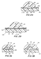
- Figure 2A illustrates a partial cross-sectional view of a hemispheric plastic bubble 94 defining two volumes of gas, large volume 96 and small volume 98.
- Integrated circuit 100 is disposed immediately below gas volumes 96 and 98 and has surface portions 102a and 102b in direct contact with the substantially discrete volumes of gas. Although present, the electrodes on surfaces 102a and 102b are not illustrated in Figure 2.
- Integrated circuit 100 is mounted on base 104. Connecting wire 106 extends between integrated circuit 100 and other components in the radiation detector located at other places on substrate base 104.
- tissue equivalent plastic is a polyethylene based plastic with mixture of carbon black, calcium fluoride, and nitrogen containing plastics that approximately match the elemental characteristics (C, N, H and O) and effective atomic number of human muscle.
- Gas volumes 96 and 98 are not illustrated as being completely isolated and further the plastic, which forms bubble 94, extends laterally along surface 108 of substrate 104. Precise isolation between volumes 96 and 98 is not required because ions generated by the radiation will move in each volume dependent upon an electric field established therein. Few if any ions pass between gas volume 96 and gas volume 98.
- the plastic is not illustrated as being specifically mounted on surface 108 of substrate 104 because of manufacturing constraints. Also, Figure 2 is a magnified view of the ion chamber and the gap between plastic 94 and surface 108 may be exaggerated in that illustration.
- FIG. 2B illustrates IC 100 mounted on substrate 104. Additionally, a thin tissue equivalent plastic insert layer 101 is interposed between bubble plastic 94 and substrate 104 by mounts 103 and 105. Tissue equivalent plastic dots 107 and 109 are chosen as the collecting electrodes in order to obtain the proper electron equilibrium in the ion chamber. The geometry of the dots can be used to optimize the electric field. Layer 101 and dots 107 and 109 are an integral part of the IC surface. Other collecting electrode materials may be used to gain different advantages.
- Plastic bubble 94 is molded to define two gas volumes 96 and 98.
- all the electronics for the radiation detector reside on one substrate.
- the ICs, one of which is IC 100, are bonded directly to the substrate.
- the circuit can be injection molded into the bottom case of the radiation detector or be a rigid board or a flexible substrate which is attached to the bottom case. It is important that the integrated circuits align with the ion chambers on the top half of the case. Also, it is important that water does not leak into the radiation detector after it is assembled.
- An adhesive type epoxy may hold the two halves of the detector together or they can preferably be welded together.
- the thickness of the thinnest chamber wall is approx. 0.076 mm (0.003 inch); therefore, further protective structures may be required for that chamber holding that volume of gas.
- Figure 3A illustrates another embodiment of the present invention wherein large gas volume 96 is immediately proximate and atop integrated circuit 100 but small gas volume 98 is disposed proximate to but offset from IC 100. Small volume 98 should be as close as possible to the IC to minimize capacitance.
- An important feature of the present invention is the presence of the collecting electrode in direct contact with the gas volume, e.g., in Figure 3A, electrode 110 in gas volume 96.
- the collecting electrode is on a surface segment of the IC.
- the surface segment is a portion of the structure which defines the volume of gas.
- the claims appended hereto include the concept that the collecting electrode may be bond pads, sense pads or electrically conductive, plastic structures bonded to, overlayed on or connected to the IC.
- the collecting electrode may encompass all of the surface segment of the IC in contact with the gas.
- the IC is in close proximity to the volume of gas and in a preferred embodiment is immediately below the volume of gas.
- a protective covering, a non-conductive layer, or other structures placed on the surface of the IC, exclusive of the surface portion having the collecting electrode thereon, is encompassed by the use of the term "integrated circuit element" in the claims.
- collecting electrode 110 (the size of which is exaggerated in Fig. 3A) is on surface 102 of integrated circuit 100 and collects the ions produced by the radiation within gas volume 96. With respect to smaller gas volume 98, collecting electrode 112 is disposed on substrate 104. In a similar fashion to collecting electrode 110, collecting electrode 112 is in direct contact with the potentially ionized gas in gas volume 98. Coupling wire 114 electrically couples collecting electrode 112 to appropriate electronics in integrated circuit 100.
- Figure 3B shows an embodiment wherein two ion chambers or gas volumes 96 and 97 are concentric and both are disposed atop IC 100.
- the lower gas volume 96 is a low dose rate ion chamber and chamber or volume 97 is the high dose rate chamber.
- the volumes are physically separated by barrier wall 95. Gas is capable of passing between volumes 96 and 97 via passage 99.
- barrier wall 95 is an electrically insulating plastic support having on its radially outer surface a collecting electrode structure (not shown but may be a layer of conductive plastic) for the high dose chamber or volume 97.
- the radially inner surface of wall 95 includes a biasing or counter electrode, which is described in detail later with respect to the electric field generating means, for the low dose chamber or volume 96.
- wall 95 is not made of electrically insulating material but is an electrically conductive plastic material such that the low dose rate counter electrode and the high dose rate collecting electrode are the same entity.
- control circuitry selects the effective range of the detector subassemblies by selecting which chamber is being monitored.
- the high dose rate chamber (volume 97) has a more uniform electric field.
- Figure 4 illustrates an alternative embodiment of the present invention showing integrated circuits 120 and 122 associated with ion chambers 124 and 126, respectively. Only a surface segment of each IC is proximate the respective volume.
- Figure 5 illustrates the top surface 128 of an integrated circuit 130. Bond pads 132 are illustrated along the right-hand portion of integrated circuit 130. These bond pads provide electrical contacts to the integrated circuit. On surface 128, electrodes E1, E2 and E3 are illustrated as being concentric.
- Figure 6 is a cross-sectional view of integrated circuit 130 which has been mounted on base 134 and below an ion chamber.
- Plastic bubble 136 defines gas volume 138.
- Electrodes E1, E2 and E3 are in direct contact with the gas in gas volume 138.
- Figure 7A shows a further embodiment of the present invention utilizing multiple ion chambers 140, 142 and 144 disposed atop integrated circuit 146.
- Ion chambers 140, 142 and 144 include electrode sets 148, 150 and 152, respectively.
- Figures 7B and 7C show a "snowman" configuration. The "snowman" configuration places the IC or a corner thereof into a fully spherical ion chamber. See IC 145 partially exposed to chamber 147 in Figure 7B. This gives almost 4 ⁇ uniform detection. The spherical volume inside the inner wall defining chamber 147 is filled with gas.
- FIG. 7C shows plastic case 141, capable of holding batteries and other components and IC 145 extending beyond the outer wall of the bubble defining chamber 147.
- an electric field is generated therein such that the ions move in accordance with the electric field.
- flux lines are illustrated as intersecting with and/or extending from the electrodes.
- the semicircular line 154 represents the interior surface of the plastic bubble of the ion chamber.
- V s is the sensing voltage and usually designates the collecting electrode; 0 v represents a grounded element; and V s1 , V s2 and V s3 represent different collecting electrodes set at different predetermined voltages.
- electrode E1 is the collecting electrode and is set at voltage +V s . It is to be understood that the voltages illustrated and discussed herein are only exemplary and any discrete voltage levels can be used in place of the described and illustrated voltages. For example, rather than having a positive voltage at the collecting electrode, a negative voltage can be applied thereto. In that case, positive ions are collected at the collecting electrode rather than negative ions as discussed with respect to a +V s , at the collecting electrode. Also, the 0 v could be any internal ground voltage other than zero volts which is designated as ground for the radiation detector.
- electrode E1 is the collecting electrode and is electrically biased to predetermined level +V s .
- V s implies that this electrode is connected to a sensing circuit.
- the voltages E n imply connection to a voltage source with no measurement of collected charge being done.
- Electrodes E2 and E3 operate as biasing electrodes and are at 0 v.
- the one end of the flux lines of the electric field in Figure 8 intersects collecting electrode E1 and the other end intersects biasing electrodes E2 and E3. Also, since interior surface 154 will be typically grounded and since the plastic is conductive in nature, the electric field does extend to that interior surface.
- the radiation detection subassembly includes means for generating the electric field.
- the strength of the electric field generally depends upon the voltage differential between the collecting electrode and another element within or without the volume of gas. Therefore, the strength of the electric field can be varied by changing the voltage differential, at least in Figure 8, between electrode E1 and electrodes E2 and E3. By applying a lower voltage to electrodes E2 and E3, the electric field within the volume of gas would increase. Similarly, by raising the voltage V s on collecting electrode E1, the electric field increases.
- interior surface 154 is grounded at 0 v, electrodes E1 and E2 are biased to voltage +V e and electrode E3 is selected as the collecting electrode and is biased to +V s . Since electrode E3 is selected as the collecting electrode, the region swept is that region between electrode E3 and surface 154 and is limited to the radially outer sectors of the volume. A complex conically cylindrically symmetric region is therefore swept.
- any one of electrodes E1, E2 and E3 can be the collecting electrode since V s1 need not equal V s2 or V s3 .
- the means for generating the electric field need not be a battery. It can be two dissimilar materials which are physically and electrically connected at one end. For example, if the ends of a piece of copper and a piece of steel are joined, a voltage develops across the free ends of the copper and steel due to the work function difference between the different materials. This voltage differential may be sufficient to create the electric field for the IC dosimeter. Particularly, a gold plate or element and a carbon based plastic may be utilized to generate an electric field in this fashion due to the work function between gold and the carbon based plastic. Also, the biasing electrodes do not have to be exposed to the gas (excepting the collecting or sensing electrodes) since a field can be developed by conductors either within the IC or within the hemispheric bubble defining the volume of gas.
- the radiation interacts with the gas in the ion chamber generating ions which move in the electric field.
- the ions of one polarity are collected on the exposed collecting electrode and the charge signal therefrom is amplified. If the collecting electrode is biased to a positive voltage with respect to the other electrodes, negative ions will be attracted and the voltage +V s will decrease based upon the amount of collected ions.
- the number of ions generated is proportional to the dose received. Ideally, all the ions generated are collected.
- the gas in the chambers should be under a slight pressure to provide some crush resistance when thin covers are used for the detection of beta particles.
- the choice of gas is determined by the energy response desired. Air, nitrogen, argon or tissue equivalent gas are possibilities.
- Roentgens The use of air would result in the radiation being measured in Roentgens (R).
- Tissue equivalent gas measures radiation in rad (radiation absorbed dose) or Gy (gray unit which equals 100 rads).
- 1 Roentgen unit (R) equals 258 ⁇ C/kg.
- the ion chamber performance is not ideal.
- the greater the radiation dose rate the greater the number of ions generated.
- the ions are not collected instantly, so the concentration of ions in the gas increases with increasing dose rate. This results in some of the positive ions recombining with negative ions. These ions cancel and are not collected by the electrodes. Thus, the charge collected is decreased by this recombination and the measurement is no longer proportional to the dose received.
- the minimum size of the ion chamber is determined by the minimum dose rate to be reliably detected.
- the dose rate permissible in an unrestricted area is 2 mR/hr.
- a reasonable charge sensitivity for an integrated circuit amplifier is 1000 electrons since engineering literature describes an amplifier that can sense 1 mv with an input capacity of 1 x 10 ⁇ 14F.
- 1 mR as being the amount of radiation required to generate 2000 ion pairs/mm3
- a volume of 180 mm3 would average one pulse every five seconds at a dose of 2 mR/hr.
- the shape of the ion chamber is controlled by the conflicting desires to have as high an electric field as possible and as low a capacitance as possible.
- the higher the electric field the faster the ions move and higher the dose rate which can be accurately monitored.
- the lower the capacitance the smaller the minimum charge and hence the smaller the dose which can be measured.
- a large area parallel plate arrangement could give the highest field. Concentric spherical surfaces would give a low capacitance. As mentioned above, at high dose rates, recombination occurs.
- Different ion chambers and measurement circuits can accurately measure different dose rates. In certain situations, monitoring needs to occur over a wide range of dose rates, such as a survey instrument, or an area monitor which must take measurements during an accident as well as normal times. Or, some information about the radiation dose as a function of energy may be needed so several ion chambers are needed.
- the high dose rate chamber would be significantly smaller and have a higher field than the low dose rate chamber.
- the collecting electrode need not be directly attached to the integrated circuit as illustrated in Figure 3.
- the added capacitance of connecting wire 114 can be tolerated because ion chamber 98 does not need to be sensitive to miniscule doses.
- the control electronics in the detector control and interface unit 14 monitor the dose rate from each detection subassembly and use the chamber which is most accurate.
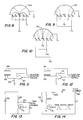
- FIG. 8 shows the bias applied when measuring a low dose rate. All charge is collected at center electrode E1. Charge is collected from the total volume.
- Figure 9 shows the bias conditions for which charge is measured in a smaller, high field, volume. In Figure 10, the collecting electrode and hence the volume swept can be selected.
- Figures 11 and 12 illustrate circuits which measure the current to the collecting electrode 155 rather than the charge due to the collection of ions on that electrode.
- one input of amplifier 157 is biased to a voltage level dependent upon the power source V1 and the value of resistor 159. The voltage changes due to the voltage drop across resistor 159 as the collected current is conducted through it.
- electrode 156 is a bias electrode that establishes the electric field in the volume of gas.
- resistor 161 provides a feedback voltage signal that is a basis for comparing the signal obtained from collecting electrode 155.
- FIGS 13 and 14 illustrate flyback circuits to increase the voltage levels and hence increase the electric field.
- the use of flyback circuits permits bias control circuitry for a particular ion chamber to increase the bias field V e(g) (depicted as V e in Figure 9) as the dose rate increases. For example, for every factor of 10 increase in the dose rate, the bias is increased by the square root of 10 to maintain recombination losses at the same level.
- the flyback transformers 160, 160a and 160b are triggered via transistor T g after the dose rate exceeds some rate threshold.
- the charge on capacitor C f is increased due to the release of energy from inductors 160 and 160a when T g is turned off.
- the battery voltage is applied to V e with substantially no voltage loss other than the diode.
- the detector control in Figure 1 can be configured to control the flyback circuits in this manner.
- This power circuitry is part of the detector control as is any required voltage regulation circuitry.
- FIGs 15, 16, 17, 18, 19, 20 and 21 illustrate electrical block diagrams for the radiation detector.
- collecting electrode 170 is electrically biased to predetermined voltage level V s .
- Bias electrode 171 establishes the electric field in the gas and is coupled to power supply 173.
- the dashed box 175 on the right indicates that those components are part of one radiation subassembly in Figure 1.
- the dashed box 177 indicates components considered part of detector control and interface unit 14 in Figure 1.
- the collecting electrode is exposed to the volume of gas.
- the collecting electrode is also the control gate for amplifying transistor T0, i.e., the collecting electrode is "incorporated" into the amplifier embodied by transistor T0.
- the source of amplifying transistor T0 is coupled to voltage V2 and the drain of the amplifying transistor places a signal on line 172 representative of the amount of accumulated charges on the electrode and hence the radiation sensed by the detector subassembly.
- Buffer amplifier 174 isolates amplifying transistor T0 from the rest of the circuitry and amplifies T0's output.
- V0 is applied to sense amplifier 176.
- Sense amplifier 176 determines when the V0 drops below a predetermined threshold V ref and generates trigger signal for counter 178.
- the trigger signal is also applied as a clearing control signal to a circuit which restores voltage V s to the collecting electrode or clears the accumulated charge from the electrode. If V s is a positive voltage with respect to the voltage on 171, negative ions will be attracted to collecting electrode 170 and voltage V0 will fall dependent upon the accumulated charge. When V0 falls below V ref , sense amplifier 176 triggers counter 178.
- Switching transistor T1 applies a clearing voltage V c1 to the control gate of amplifying transistor T0. Clearing voltage V c1 is developed across capacitor C1. Switching transistor T1 is turned on by the clear control signal, i.e., the trigger signal, from sense amp 176 and thereafter couples capacitor C1 to the control gate of amplifying transistor T0. During the trigger pulse, inverter 180 turns second switching transistor T2 off and therefore isolates V chg from capacitor C1. When the trigger signal is removed, second switching transistor T2 is turned on and capacitor C1 is charged by voltage V chg . It is recommended that transistors T1 and T2 do not conduct at the same time. In this sense, the turn off time of the transistors must be quick and the turn on time must be slow.
- transistors T0, T1 and T2 as well as buffer amplifier 174, sense amplifier 176, counter 178 and capacitor C1 are all disposed within the integrated circuit.
- the buffer and sense amplifiers may be combined.
- Other data processing components in the detector control and interface unit are downstream of counter 178 and may or may not be on the same IC.
- Collecting electrode 170 is directly exposed to the volume of gas and may be embodied as a sense pad which is placed above a conductive channel running internally into the integrated circuit element.
- the sense pad may be larger than the internal conductive channel because the sense pad can be spread over a top layer of insulation on the surface of the integrated circuit.
- CMOS technology can be utilized to obtain the low power detector described herein.
- sense amp 176 is part of amplifier 20; counter 178 corresponds to part of calculator and controller 30, transistors T1 and T2 and associated circuitry correspond to charge removal device 26.
- Counter 178 can be reset or re-zeroed on a periodic clock signal from computer 30.
- the device control and interface unit could operate on purely analog signals from the subassemblies rather than digital signals. As is described in detail below, the charge removal, the electric field generation and leakage compensation are all interrelated.
- switching transistor T1 to provide a clearing voltage (V c1 ) to the control gate of amplifying transistor T0 presents a problem regarding the current leakage, ILEAK, from the transistor diffusion to the IC substrate.
- the current leakage is designated by dashed lines as ILEAK in Figure 15 from the integrated circuit substrate to the drain of switching transistor T1.
- This current leakage ILEAK will be sensed as an accumulated charge and hence a dose. A rough calculation indicates that this leakage could cause a pulse every eight seconds. For a 0.18cm3 chamber, this gives a background reading of radiation of 1.25 mR/hr which is unacceptable. The effect of leakage should be less than 1 mR/day. Corrective measures for minimizing the effect of ILEAK are discussed later.
- Figure 16 illustrates collecting electrode 170 and biasing electrode 182 as well as a rate change circuit that includes transistor T R . Items to the left of the double dashed line 85 are considered part of the detection subassembly; items to the right are part of the detector control.
- the biasing voltage V e is applied to biasing electrode 162 providing an electric field that extends between collecting electrode 170 and biasing electrode 182.
- the bias voltage can be controllably set by a control circuit 184 coupled to the output of counter 178.
- biasing voltage V e can be controllably set at a plurality of discrete levels dependent upon the count in counter 178.
- the flyback circuits of Figures 13 and 14 could be used to apply this increased biasing voltage.
- Transistor T r is controlled by rate change control signal TR gate from control circuit 184.
- rate change control signal TR gate is high, capacitor C r is electrically coupled to the control gate of transistor T0. Therefore, accumulated charge on collecting electrode 170 must charge or discharge capacitor C r and hence the rate at which signal V0 changes is decreased because of the added capacitance.
- the electronics has a maximum count rate set by its speed. If this maximum count rate becomes a limitation rather than the charge recombination rate discussed earlier, it is necessary to add the extra capacitance C r to reduce the sensitivity of the detection subassembly.
- C r When transistor T r is conductive, the amount of charge required to trigger sense amp 176 is increased.
- the control circuit 184 would monitor the dose rate and provide rate change control signal TR gate when the dose rate exceeds a predetermined level.
- the major difficulty with clearing or restoring voltage V s to the control gate of transistor T0 via transistor T1 is the current leakage ILEAK from the integrated circuit substrate to the drain of transistor T1 and hence the collecting electrode.
- the rough estimate earlier presented indicates that this leakage may cause a pulse every eight seconds.
- One method of compensating for ILEAK is simply to have the radiation detector not register any pulses unless the pulses are less than eight seconds apart. This operation is simply pulse stream manipulation.
- a second simple method is to have the radiation detector not register any dose when it is disabled or turned-off. The detector could be stored in a charging/disabling cradle during that time.
- Figure 17 illustrates a block diagram circuit for analog current subtraction used to compensate for the leakage current.
- Current generator ICOMP is controlled by ICOMP control 186.
- the ICOMP control would be sent during calibration of the detector.
- ILEAK would be a current source and ICOMP would be a current sink.
- ICOMP is controllable by ICOMP control 186.
- the difficulty with this system is having ICOMP follow ILEAK as conditions vary.
- FIG 18 illustrates another alternative embodiment of a circuit to compensate for ILEAK.
- the sensing circuit is indicated by character “a” such that transistor T0 is now T 0a .
- T 0a is coupled to buffer amplifier 174a, sense amp 176a and counter 178a.
- a duplicate circuit is illustrated with character “b.” Therefore, the counterpart to transistor T 0a is T 0b , buffer amp 174a is duplicated as amp 174b, etc.
- the primary distinction between the duplicate circuit and the sensing circuit is that the control gate for transistor T 0b is not coupled to the collecting electrode in the duplicate circuit.
- T 1a and T 1b are equal in size and do not contain any gross defects
- the leakages ILEAKA and ILEAKB should be almost identical. In other words, both leakage currents should track each other as conditions vary. Therefore, the true dose exposure can be determined by taking the difference between the number of pulses received by circuits a and b.
- One compensation method utilizes a rate compensator 188. It senses when the pulse rate in sense amp 176a is less than the pulse rate in sense amp 176b and prevents an incrementing counter 178a. Thus, no dose is registered unless it is in excess of ILEAKB.
- a second method is better adapted to proportional but unequal ILEAKA and ILEAKB.
- a prescaler 190 decrements counter 178a when the count value from duplicative counter 178b equals the compensation count value in leakage compensation memory 192.
- the scaling circuit compensates for the measurement circuits not being identical.
- the leakage compensation memory is loaded during calibration and contains the proportionality constant related to the two circuits leakages.
- Figure 19 illustrates a further circuit, in block diagram form, for eliminating switching transistor T1 and thus the source of leakage.
- the collecting electrode is only connected to the control gate of transistor T0.
- the bias V e(t) drives a charge of one polarity to the collecting electrode 170.
- the single polarity charge accumulates ions at collecting electrode 170 until sense amplifier 176 triggers counter 178.
- Control circuit 184 changes the bias signal applied to bias electrode 182 thereby switching the electric field in the volume of gas to bring ions of the opposite polarity to collecting electrode 170.
- the oppositely charged ions cancel the previously accumulated charge on collecting electrode 170.
- the minimum voltage V e (t) (min) is less than V s which in turn is less than the maximum voltage V e (t) max .
- the reference voltage V ref (t) is varied such that the sense amp triggers the counter when signal V0 exceeds a maximum threshold level in one instance and falls below a minimum threshold level in a second instance. Therefore, either the reference voltage must be switched within sense amp 176 or electrical circuitry be designed to determine when V0 passes beyond a predetermined window.
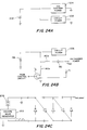
- FIG 20A illustrates a block diagram circuit which changes the voltage of collecting electrode 170 via a coupling capacitor C0.
- control circuit 194 switches coupling voltage V coup1 (t) to a different predetermined level. Therefore, the voltage V s is biased to a high and then a low predetermined level based upon a level control signal applied to level control circuit 194.
- the biasing voltage V e applied to biasing electrode 182 is at an intermediate level as compared to the maximum coupling voltage V coup1 (t) max and the minimum coupling voltage V coup1 (t) min . Switching via the coupling capacitors is advantageous because all ion chambers can have the same counter electrode potential (V e ) and the coupling capacitor is part of the integrated circuit.
- Figure 21 shows a block diagram of another circuit for clearing the accumulated charge on the collecting electrode.
- Figure 22 shows the timing diagram for the operation of the circuit in Figure 21.
- the polarity of the electric field is reversed periodically (see V z in Figure 22) similar to the operation described in Figure 19, i.e., when V D reaches V revL or V revH or effectively after a certain number of counts.
- Sense amplifiers 176a and 176b trigger a counter or other detector control component when the signal exceeds or falls below one of two reference voltages V ref1 or V ref2 .
- capacitor C D the frequency at which field reversal is required is greatly reduced, if each time the threshold is exceeded, the voltage V D is changed in a stepwise manner.
- the relatively small voltage step restores the voltage of the amplifier input to its original value (see V c between times t1 and t2) and prepares the amplifier to sense another pulse.
- This circuit substantially eliminates any inaccuracy which arises when the field polarity is changed after each pulse. Also, it confers some noise resistance similar to that given by constant charge removal versus constant voltage reset.
- a change in V D indicates one pulse sensed by one of the sense amps. From times t1 to t2, these pulses represent charge sensed and thus dose received. From times t2 to t3, the pulses are simply a result of the changing V z being capacitively coupled to V c .
- guard ring as one of the electrodes (for example, E3) around the sensing pad (for example, E1 or E2) to minimize leakage over the silicon dioxide layer in the integrated circuit and the passivation materials on that integrated circuit.
- One method of compensating for stray capacitance and stray electric fields developed by components internal of the integrated circuit is to have the guard electrode at the same potential as the sensing electrode. The geometry of the guard and the sensing electrode would be chosen such that the guard receives few of the flux lines of the electric field but surrounds the sensing electrode, thereby interrupting any surface leakage from the internal components.
- any of these methods of leakage compensation can be combined with any ion chamber described above.
- a large ion chamber would utilize integrated circuit control without switching transistor T1 and utilize electric field reversal.
- the same or a different integrated circuit senses the accumulated charge from a second smaller ion chamber utilizing the simplest sensing circuit illustrated in Figure 15. No leakage compensation is necessary in this simple circuit because the count from the small ion chamber is recognized only if the dose rate is high. Also, in the contamination monitor discussed previously, this ion chamber configuration would be repeated for each of the three tissue depths at which a measurement is to be made.
- Figure 23 is a further development from Figure 10.
- selector control 196 actuates selecting means 200 which selects one of the electrodes E1, E2 or E3 as the collecting electrode.
- the accumulated charge from the selected collecting electrode would be applied via T s1 , T s2 or T s3 to buffer amplifier 174.
- biasing electrodes could be selected to apply different levels of biasing voltage for the electric field at different times. Because different volumes of the gas are swept by the electric field of the different electrodes, changing the biases and the collecting electrode changes the sensitivity and dose rate limits of the radiation detector.
- Figures 24a, 24b and 24c illustrate power circuits for the detector.
- the power from battery 202 is applied directly to ion chamber power 204 as well as to circuit power 206.
- Figure 24c illustrates a capacitive voltage multiplier which increases battery voltage without the need for an inductor.
- Square wave generator 210 activates the set of capacitors to achieve this multiplication of voltage.
- Figure 25 illustrates, in block diagram form, the memory and communications section in the detector control.
- this section is associated with one IC.
- This communications section is a means for recovering the radiation count from the counters.
- the dashed line 212 indicates an interface with a bus structure for transferring data and command or control signals between the memory and communications sections for other ICs.
- all the integrated circuits are connected as is best illustrated in Figure 26, the power and communication path diagram.
- the alarm out line is activated if any one of the ICs, IC1, IC2 or IC3, generates an alarm.
- the alarm is passed from IC to IC by the alarm-in/alarm-out interconnection between the three integrated circuits.
- the alarm is passed to the human interface 34 in Figure 1 when the radiation detector is, for example, configured as an area alarm monitor or as a contamination monitor.
- the data out line is coupled to the electronic interface 36 when the radiation detector is configured as a survey meter or an exposure rate meter. In the latter configurations, the chip enable command would be periodically actuated to provide a seemingly continuous radiation readout.
- the alarm-out line is raised when any line coupled to OR gate 214 is raised: the alarm-in line, the dose alarm/rate alarm line from the control circuit/radiation count counters or the cyclic redundant character (CRC) control check circuit 216.
- CRC cyclic redundant character
- Memories M1, M2, M3, M4, M5, M6, M n-3 , M n-2 , M n-1 and M n are coupled to various counters and other devices in the integrated circuit.
- counter 178 (Fig. 15 and others) may be directly coupled to one of these memory units or may be the memory unit M n .
- Counter 178 and control circuit 184 must include some type of memory to trigger the control signal g (see Fig. 14), the change rate signal TR gate (see Fig. 16), the ICOMP control (see Fig. 17) and the level and pulse duration of V e(t) (see Fig. 19) and the coupling voltage (see Fig. 20).
- the leakage compensation memory is a memory unit.
- Shift registers S1, S2, S3, S4, S5, S6, S n-3 , S n-2 , S n-1 and S n are connected to corresponding memory units. These serially connected shift registers are supplied with data on the data-in line.
- the CRC space control device 218 is needed to hold the 16 CRC characters used to confirm accurate data reception without displacing any data from its proper locations. All of the serially connected registers are loaded during a data write routine and a shift register write (SRW) control signal from counter 220 loads the shift register data into the appropriate memory. Shift control to each shift register is also accomplished by a control line from counter 220.
- SRW shift register write
- Counter 220 is activated by a chip enable signal and a clock signal which is fed to AND gate 222. The output of the counter is also fed to CRC calculator 224 to indicate when to calculate and output, or check, the CRC.
- the control input/output circuit 226 is coupled to the chip enable line and to the output of the CRC checker circuit 216. I/O control 226 activates transistor T out and allows the data to be reflected on the data-out line. Also, when the counter 220 determines that the last 16-bit word is appropriately checked, it places a value of the CRC calculator 224 on the data-out line. The last 16 bits represent the CRC code which is used by the receiving device to determine if the transmission was accurately received.
- Data can be shifted into memory with a shift register read/write control line. When the read or write operation is completed for the present chip, the next chip is enabled. To write data from outside, data is shifted from M x to S x by the shift register read/write control line. Then the shift registers are shifted once on each clock cycle with one bit coming out and also going to the CRC calculator 224. When all the data is out, the 16-bit CRC is shifted out.
- Figure 26 illustrates the power and communication path for the detector with integrated circuits IC1, IC2 and IC3. Power and ground are applied from an internal battery in the detector control unit.
- the alarm is a daisy chained signal. If the alarm is active, it gets passed along. The active alarm signal out of the last chip turns the piezoelectric buzzer on if the detector is configured with an active human interface.
- the alarm could trigger a communications transmit command through the electronics interface. Upon receipt of this transmit command, the detector would transmit radiation data, e.g., dose or dose rate, to an external device. Data read and write is synchronized by the clock. The clock and all power for the external communication drivers and internal shift register is provided by communications power which is in turn supplied by a calibration and display unit.
- the chip enable and read line are held low.
- the read/write is brought high for X clock cycles and then low. After Y cycles, the chip enable is brought high. Z cycles later, all data in the IC1 is shifted serially out the data-out line. When IC1 is done, it enables IC2. Z cycles later, the data from IC2 comes out on the data-out line.
- the dosimeter counters are disabled.
- the read/write control line is held high and kept high. After A cycles, the chip enable is brought high. After B cycles, the data is serially read in on the data-in line until all shift registers are full. When IC1 is loaded, it raises the chip enable of IC2. When all the data is loaded, bringing the write line low before lowering the chip enable line causes data to be stored into the integrated circuit chip memories.
- Figure 27 illustrates detector unit 310 having ion chambers 312, 314a, 314b, 314c, 314d, 314e and 314f.
- the large ion chamber 312 is most sensitive to radiation.
- the smaller chambers 314a through f are less sensitive but are capable of accurately detecting higher doses and dose rates as compared with the larger chamber.
- the ion chambers inside domes 312, 314 and 317 may all be identical and so have identical dose rate responses, but have different wall thicknesses and, thus, be measuring dose at different depths into the body.
- Electrical contacts 320 extend from one end of unit 310.
- External connections 320 on detector unit 310 are provided to facilitate the transfer of information, i.e., radiation data, control commands, ground and power signals as necessary.
- information i.e., radiation data, control commands, ground and power signals as necessary.
- the use of output drivers in the detector unit that obtain power from an external battery in a cradle display unit 322 prevents the possibility that one or more contacts 320 would short together and result in a spark or drain of the internal battery in the detector unit.
- the only common connection between the internal circuitry in the detector unit and the external unit such as display unit 322 is ground.
- data communications can use an optical link, encoded sound, near or far field electromagnetic waves, rather than electrical contacts.
- a cradle, interface and display unit 322 is separably mated with detector unit 310.
- display unit 322 includes lip portions 324 which mate with ledge or flange 326 on detector unit 310.
- Display unit 322 includes LCD display 328 and recessed control buttons 330.
- Electrical contacts 320 on detector unit 310 mate with complementary electrical contacts not shown in display unit 322.
- the illustrated connection 323 to central control is optional since the mated detector and display units can operate as a stand alone apparatus or can operate in conjunction with multiple mated units.
- the radiation detector unit is separably mated to display unit 322 in order to allow the detector unit to be regularly tested and appropriately calibrated.
- the display unit and detector unit can be permanently mated in order to provide a survey meter, a contamination monitor or other types of radiation monitors requiring substantially continuous or controllably displayble radiation data displays.
- the geometric configuration of ion chambers 312 and 314a-f is only exemplary.
- the ion chambers can be geometrically configured in as many shapes as are permitted by manufacturing constraints.
- a grid, barrel or hemispheric geometric configuration may be appropriate, respectively, for a contamination monitor, directional survey meter and a wide area survey meter.
- Display 328 is a means for recovering the radiation count from the counters.
- Display unit 322 can also be configured as a programming device to set threshold limits, e.g., dose and dose rate thresholds, in the detector unit.
- Control buttons 330 can be utilized to confirm the thresholds input via the buttons and then confirm a successful programming of the detector unit. Since unit 322 can be viewed as a programming device, that unit is referred to herein as a programming and display unit.
- FIG. 28 illustrates, in block diagram form, the electrical components of programming and display unit 322.
- Battery 334 is coupled to an optional voltage regulator 336 which supplies voltage V supply to microcomputer on a chip 338 (herein microcomputer chip 338) and to connector pin unit 340.
- Connector pin unit 340 matingly couples with pin unit 320 of the detector unit 310.
- Microcomputer chip 338 is coupled to input buttons 342 and display unit 344. Microcomputer chip 338, when activated by input buttons 342, generates a data transfer command to detector unit 310. This transfer command is the read command discussed above with respect to Figures 25 and 26. The output from the detector unit is placed in a memory which is part of microcomputer chip 338. Also, the radiation data from the detector control interface, e.g., the counters, is displayed on display 344. Microcomputer chip 338 also programs threshold values into detector unit 310. For example, microcomputer chip 338 programmably sets the total dose alarm threshold, the dose rate threshold and the trigger threshold for the counter. The total dose alarm threshold is that radiation count value which, when exceeded, triggers the audible and electrical alarm in the radiation detector.
- Figure 29 illustrates a calibration and display device 350.
- the radiation detector is placed in either of two mounting positions, the calibration position 352 or the readout position 354.
- Calibration unit 350 includes display device 356 and keyboard 358.
- Printer 360 provides a printed copy of the information obtained from the IC dosimeter. Particularly, during calibration, a predetermined amount of radiation, from radiation source 357 (shielded by shield 359), is directed toward the detector unit.
- Calibration unit 350 monitors the resulting radiation data (both total dose and dose rate as necessary) and then compares that radiation data against accurately predetermined radiation data. This computation is carried out in microcomputer 362. The detector would then be programmed such that the threshold level of the sensing amplifier (a threshold determining means) would be set and further the alarm threshold levels for the alarm circuitry would be set by calibration unit 350.
- calibration unit 350 When the radiation detector unit is in readout position 354, calibration unit 350 would generate a transfer data command to the detector and read out all data including the current radiation data from the memory units. Appropriate information is displayed on display 356 and printed out by printer 360. Additionally, calibration unit 350 could program a date of calibration into the radiation detector unit as a historical indicator in the detector's memory. The calibration unit also resets or clears selected counters, if necessary, in the detector. Additionally, the calibrator includes a memory, clock, analog and digital interface circuits, and an I/O computer communications port to transfer data information to other computer devices.
- Figure 30 illustrates an area monitor which utilizes a plurality of radiation detectors DET1, DET2, DET3 and DET4 mounted on a support wherein DET1 is illustrated as directionally oriented or facing one region and the others are facing the opposite region.
- the radiation detectors are plugged into complementary electrical connectors 364 of area monitor 366.
- area monitor 366 utilizes at least four radiation detectors disposed 360° around an area monitor.
- a multiple IC detector control 368 periodically obtains the radiation count values from IC detectors DET1, DET2, DET3 and DET4 by issuing appropriate transfer commands; accumulates the data and relates the data to the particular detector actuated thereby indicating direction, and relates the data to date and time information; and during other occasions periodically communicates via communications circuit 372 to an external command unit.
- Area monitor 366 would include its own power source 374 to enable the area monitor to be self-sufficient and to power the detectors.
- Area monitor 366 is generally an environmental monitor which provides information regarding the direction as well as the amount of the radiation.
- a further embodiment of the area monitor is the addition of air blower or air pump 410 coupled to air monitor interface 412. By forcing air over radiation detector DET1 320, the monitor measures the amount of radiation in the air.
- an activated absorbing substance 411 can be interposed in the path of the forced air to trap particles or gases therein. Radiation detector 1 is mounted proximate absorbant 411 to measure the radiation output therefrom.
- the radiation detector may include some components to eliminate the possibility of data loss.
- An EEPROM on the integrated circuit could be utilized such that battery failure does not result in a loss of data.
- the radiation detector could chirp a "low battery" signal when the internal battery reached a predetermined low value.
- the human interface alarm, sounded by the detector could include a visual alarm as well as an audible alarm.
- the alarm signifying an overexposure of radiation (total dose) could be different than the alarm signifying an unacceptably high dose rate, i.e., different intensity, frequency and/or duty cycle.
- transistor T0 may be part of a differential amplifier or the collecting electrode may be a voltage follower input.
- Transistors T1 and T2 may be two of many additional transistors.
- the audible alarm could require a square wave generator as illustrated in Figure 24.
- This concept can be applied to radiation detectors which presently use Geiger-Mueller tubes, scintillators and photomultipliers, or solid state detectors where the decreased absorption of a gas filled ion chamber, when compared to a solid material, is not important. Also, due to their low input capacitance and resulting high sensitivity, the radiation detectors can replace proportional counters which use multiplication within the gas.
- This concept can also replace passive detectors, such as film or thermoluminescent detector material, in applications or apparatus where immediate readout would be advantageous. This includes but is not limited to radon monitoring and occupational monitoring.
Landscapes
- Spectroscopy & Molecular Physics (AREA)
- Health & Medical Sciences (AREA)
- Life Sciences & Earth Sciences (AREA)
- General Physics & Mathematics (AREA)
- High Energy & Nuclear Physics (AREA)
- Molecular Biology (AREA)
- Physics & Mathematics (AREA)
- Measurement Of Radiation (AREA)
- Investigating Or Analyzing Materials By The Use Of Electric Means (AREA)
- Other Investigation Or Analysis Of Materials By Electrical Means (AREA)
- Electron Sources, Ion Sources (AREA)
- Measurement Of Current Or Voltage (AREA)
- Photoreceptors In Electrophotography (AREA)
Abstract
Description
- The invention refers to a radiation detector means for measuring radiation comprising the features according to the preamble of
claim 1. - A radiation detector means of the aforementioned art is known from IEEE Transactions on Nuclear Science (Vol. NS26, No. 4, August 1979, pages 4596 ff.), wherein the radiation detector means is named multichannel electrometer system. This known electrometer comprises an array of ionization chambers which are closely spaced by about 2 cm. An essential disadvantage of this electrometer is the separation of the different ionization chamber detectors and their corresponding electrometer circuitries. Therefore, cables etc. are necessary for the connection of the ionization chambers and the electrometer circuitries. Additionally, each electrometer is housed in a cast-aluminium box. These disadvantages therefore do not allow a high accuracy in measuring the corresponding radiation.
- Ionizing radiation presents a direct hazard to people; therefore, the measurement of radiation in environmental settings is important. The type of radiation monitor or detector used to measure the radiation depends upon the type of radiation, e.g., beta, alpha or X-ray and the environmental setting, e.g., an environmentally isolated laboratory, an open mine, a waste dump holding potentially hazardous material. The laboratory most likely requires a monitoring system with a continuous display and singular or multiple radiation detectors; the mine requires a moderately sensitive portable area detector; and the waste dump a relatively sensitive, directional detector.
- D. A. Waechter et al. describe in an article entitled "New Generation Low Power Radiation Survey Instruments," a standard portable dosimeter (radiation monitor) system. The portable monitor consists of a Geiger-Muller tube (GM tube) with an event counter which records the number of ionizing events. There is a readout display and an audio alarm. The problem with the GM tube is that its response is not linear with the energy of the radiation so its accuracy varies with radiation energy, although it is useful for warning.
- It is a main object of this invention to provide a radiation detector means which accurately measures both the total radiation exposure (total dose) and the rate of exposure (dose rate).
- It is another object of the present invention to provide small, lightweight, integrated radiation detector means which electronically record the degree of radiation exposure.
- It is an additional object of the present invention to provide a radiation detector means which is separably mounted in a calibration and display unit capable of calibrating the assembly and displaying the radiation count or the dose rate.
- It is an additional object of the present invention to provide a radiation detector means usable whenever ionizing radiation needs to be detected and measured, for example, area monitors, survey notes, radioactive gas detectors and quality assurance measures.
- The aforementioned main object is solved by the features of
claim 1, while the further objects will be solved by the dependent claims. - In one embodiment, the radiation detector means includes at least one radiation detection sub-assembly and a detector control means and interface unit. Each subassembly includes a hemispheric bubble of electrically conductive tissue equivalent plastic which defines a volume of gas within the bubble. The gas is adapted to be ionized by radiation incident thereon. An integrated circuit (herein IC) is mounted below the volume of gas. A collecting electrode, on the surface of the IC, is in direct contact with the gas and collects ions resulting from the ionization of the gas by the radiation. The IC includes an amplifier that incorporates the collecting electrode. The detector control and interface unit conditions the signal from the amplifier and buffers that signal. In one embodiment, the unit includes a sensing amplifier that acts as a comparator, and a counter which is used to control the detection subassembly. The collecting electrode is a control gate for an amplifying transistor in the incorporated amplifier. An electric field within the volume of gas moves ions of one polarity toward the collecting electrode. The control gate/collecting electrode is biased to a predetermined level which changes due to the collected ions and therefore the output of the amplifying transistor is a signal representative of the amount of ions collected. The signal is applied to the interface and passed to the sense amplifier. When the conditioned signal passes a predetermined threshold, the counter is triggered and is incremented. Triggering the counter also commands a circuit to clear or restore a predetermined bias level to the control gate (the collecting electrode) of the amplifying transistor. The interface may additionally include a dose and dose rate computer, a memory and a communications section. In further embodiments, the voltage level (bias) of the collecting electrode is switched from a high and to a low level or vice versa upon receipt of a triggering pulse, thereby eliminating the need to electrically connect a voltage source to the collecting electrode to clear the accumulated charge.
- Multiple electrodes can be used on the surface of the IC and configured either as collecting electrodes or biasing electrodes. In the latter configuration, the flux lines of the electric field extend between the biasing electrodes and the collecting electrodes. Otherwise, the electric field extends between the collecting electrodes and the interior surface of the conductive plastic defining the bubble of gas.
- Another embodiment of the present invention utilizes several volumes of gas disposed above a single IC. In this setting, the IC has a plurality of collecting electrodes in direct contact with each volume of gas. In an additional embodiment, one volume of gas is displaced from atop the IC by a small distance. In this situation, the IC and the corresponding collecting electrode in the offset volume of gas are mounted on the substrate. The electrode is electrically coupled to the amplifier in the IC.
- The radiation detector may be used in a calibration and display device. Further, a plurality of radiation detectors can be configured as an area network.
- The invention, however, together with further objects and advantages thereof, may best be understood by reference to the following description taken in conjunction with the accompanying drawings in which:
- Figure 1 illustrates a functional block diagram of the radiation detector;
- Figures 2A and 2B illustrate a partial cross-sectional view of two volumes of gas, or ion chambers, atop an integrated circuit;
- Figure 3A illustrates another embodiment wherein one chamber is disposed proximate to but offset from the integrated circuit;
- Figure 3B illustrates an embodiment wherein two ion chambers are concentric and both are disposed atop the integrated circuit;
- Figure 4 illustrates a cutaway top view of an embodiment of the present invention showing ion chambers atop two integrated circuit elements;
- Figure 5 illustrates the integrated circuit having surface electrodes E₁, E₂ and E₃;
- Figure 6 illustrates the cross-sectional view of the ion chamber with multiple electrodes E₁, E₂ and E₃, in direct contact with the gas in the chamber;
- Figures 7A, 7B and 7C illustrate respectively multiple ion chambers per IC and multiple chambers each having a corresponding IC;
- Figures 8, 9 and 10 schematically illustrate the electric field configurations with multiple electrodes in an ion chamber;
- Figures 11 and 12 illustrate circuits, in block diagram form, which measure the voltage of the sensing or collecting electrode;
- Figure 13 illustrates a flyback circuit which applies an increased voltage bias to a bias electrode;
- Figure 14 illustrates another flyback circuit;
- Figure 15 illustrates a block diagram circuit for measuring the amount of radiation and counting the radiation dose;
- Figure 16 illustrates a block diagram circuit that changes the rate at which the voltage changes on the collecting electrode dependent upon the radiation count;
- Figure 17 illustrates a block diagram circuit for compensating current leakage between the drain of switching transistor T₁ and the IC substrate;
- Figure 18 illustrates further leakage compensation circuit;
- Figure 19 illustrates a block diagram circuit that varies the voltage bias applied to the bias electrode thereby eliminating the switching transistor;
- Figures 20A and 20B illustrate a block diagram circuit that changes the voltage level applied to the collecting electrode and the timing diagram therefor, respectively;
- Figure 21 illustrates a block diagram circuit that changes both voltage levels applied to the bias electrode and the collecting electrode.
- Figure 22 shows a timing diagram for the circuit in Figure 21;
- Figure 23 illustrates multiple electrodes coupled to a selecting means in block diagram form;
- Figures 24a, 24b and 24c schematically illustrate a power circuit, a flyback circuit and a capacitive voltage multiplier for the present invention;
- Figure 25 illustrates a memory and communications section for the radiation detector;
- Figure 26 illustrates the power and communications paths for multiple integrated circuit elements in the detector;
- Figure 27 illustrates an exploded view of the radiation detector and a cradle display unit which mates with the detector;
- Figure 28 illustrates a block diagram circuit for the display unit;
- Figure 29 illustrates a detector calibration and display device; and,
- Figure 30 illustrates an area monitor utilizing four detectors.
- This invention relates generally to a radiation detector and particularly to a radiation detector with a volume of ionizable gas atop a solid-state integrated circuit.
- Figure 1 illustrates a functional block diagram of the radiation detector. Radiation detector 10 includes two general sections, a
radiation detection assembly 12 and a detector control andinterface unit 14.Radiation detection assembly 12 includesradiation detection subassemblies detection subassembly 1. Anion chamber 16 holds a volume of ionizable gas atop an integrated circuit having a collecting or sensing electrode in direct contact with the gas. Afield generator 18 develops an electrical field within the volume of gas and moves the ions in the gas created by radiation. The signal from the collecting electrode is applied toamplifier 20 and is subsequently applied to a leakage compensation and dischargecontroller₁ 22 in detector control andinterface unit 14. The leakage compensation is discussed in detail below with respect to Figures 15 through 18. Alternatively, or in addition to, thedetection subassembly 1 may include leakagecompensation circuit A 24. Since the collecting electrode attracts ions in the gas due to the bias placed thereon, the subassembly includescharge removal device 26 that is coupled to the input ofamplifier 20 and the input offield generator 18. The specific circuitry forcharge removal device 26 and its operation is described later with respect to Figures 15 through 22. - Leakage compensation and discharge
circuit₁ 22 controlscharge removal device 26. In the detector control andinterface unit 14, a leakage compensation and discharge circuit is associated with each radiation detection subassembly. Leakage compensation and dischargeunit₁ 22 is coupled to dose and dose rate calculator andcontroller 30,memories 32,human interface 34 andelectronic interface 36. The dose and dose rate calculator and controller generally determines the total amount of radiation the radiation detector has been subjected to as well as the rate at which the detector detects the radiation. These items are stored as radiation count data in thememories 32. The radiation detector may be embodied as CMOS integrated circuit elements to reduce power requirements and hence reduce the size of a power supply. The power can be internal to the detector and can be a battery; the power supply and the battery are not shown in Figure 1. Various detection subassemblies and associated circuits in the detector control can be embodied as a plurality of integrated circuits (ICs). These ICs can be coupled to a microcomputer on a chip that functions as dose and dose rate calculator andcontroller 30,memories 32,human interface 34 andelectronic interface 36. In another embodiment, a substantial portion of the detector can be embodied as a single IC. In general, thehuman interface 34 can include a display device which displays the total radiation count, i.e., the dose, or the dose rate. The human interface could also include actuable switches such that the dose and dose rate could be displayed upon command. Alternatively, those values could be continuously displayed. Further, the human interface may include alarm circuitry which would audibly, visually or otherwise (such as tactile or olfactory) provide an alarm to a human indicating that a certain dose threshold or a dose rate threshold has been exceeded.Electronic interface 36, in another preferred embodiment, could include a communications section linking a plurality of radiation detectors together. The electronic interface in combination with calculator andcontroler 30 andmemories 32 could provide for the setting or programming of the dose threshold or dose rate threshold for the alarm. Calculator andcontroller 30 is the controller forinterfaces memories 32, and the other components inunit 14. - In another alternative embodiment,
detection subassemblies Detection subassembly 1 could detect significantly lower levels of radiation thansubassembly 2 and calculator andcontroller 30 can be programmed to select the output fromsubassembly 2 only after the output ofsubassembly 1 reaches a predetermined value. In a general sense, detector control andinterface unit 14 buffers the signal fromradiation detection assembly 12 and conditions the output signal from those subassemblies as well as processes those output signals. - Figure 2A illustrates a partial cross-sectional view of a
hemispheric plastic bubble 94 defining two volumes of gas,large volume 96 andsmall volume 98.Integrated circuit 100 is disposed immediately belowgas volumes surface portions surfaces Integrated circuit 100 is mounted onbase 104.Connecting wire 106 extends betweenintegrated circuit 100 and other components in the radiation detector located at other places onsubstrate base 104. - It is known to persons of ordinary skill in the art that the domestic and international government regulations require and/or recommend measuring dose at different tissue depths. Therefore, several ion chambers are included in the radiation detector. The geometry of each ion chamber can be altered to match the radiation response of the human body. Likewise, different wall materials can be used rather than tissue equivalent plastic. Also, different types of gas can be utilized to vary the detection of prescribed types or energies of radiation. The thickness of the ion chamber wall, if made from tissue equivalent plastic, determines the depth, into the human body, at which the radiation is being measured. An example of tissue equivalent plastic is a polyethylene based plastic with mixture of carbon black, calcium fluoride, and nitrogen containing plastics that approximately match the elemental characteristics (C, N, H and O) and effective atomic number of human muscle.
-
Gas volumes bubble 94, extends laterally alongsurface 108 ofsubstrate 104. Precise isolation betweenvolumes gas volume 96 andgas volume 98. The plastic is not illustrated as being specifically mounted onsurface 108 ofsubstrate 104 because of manufacturing constraints. Also, Figure 2 is a magnified view of the ion chamber and the gap betweenplastic 94 andsurface 108 may be exaggerated in that illustration. - Figure 2B illustrates
IC 100 mounted onsubstrate 104. Additionally, a thin tissue equivalentplastic insert layer 101 is interposed betweenbubble plastic 94 andsubstrate 104 bymounts 103 and 105. Tissue equivalentplastic dots Layer 101 anddots -
Plastic bubble 94 is molded to define twogas volumes IC 100, are bonded directly to the substrate. The circuit can be injection molded into the bottom case of the radiation detector or be a rigid board or a flexible substrate which is attached to the bottom case. It is important that the integrated circuits align with the ion chambers on the top half of the case. Also, it is important that water does not leak into the radiation detector after it is assembled. An adhesive type epoxy may hold the two halves of the detector together or they can preferably be welded together. The thickness of the thinnest chamber wall is approx. 0.076 mm (0.003 inch); therefore, further protective structures may be required for that chamber holding that volume of gas. - Figure 3A illustrates another embodiment of the present invention wherein
large gas volume 96 is immediately proximate and atopintegrated circuit 100 butsmall gas volume 98 is disposed proximate to but offset fromIC 100.Small volume 98 should be as close as possible to the IC to minimize capacitance. - An important feature of the present invention is the presence of the collecting electrode in direct contact with the gas volume, e.g., in Figure 3A,
electrode 110 ingas volume 96. The collecting electrode is on a surface segment of the IC. The surface segment is a portion of the structure which defines the volume of gas. However, the claims appended hereto include the concept that the collecting electrode may be bond pads, sense pads or electrically conductive, plastic structures bonded to, overlayed on or connected to the IC. In a strict sense, the collecting electrode may encompass all of the surface segment of the IC in contact with the gas. In any case, the IC is in close proximity to the volume of gas and in a preferred embodiment is immediately below the volume of gas. A protective covering, a non-conductive layer, or other structures placed on the surface of the IC, exclusive of the surface portion having the collecting electrode thereon, is encompassed by the use of the term "integrated circuit element" in the claims. - Returning to Figure 3, collecting electrode 110 (the size of which is exaggerated in Fig. 3A) is on
surface 102 ofintegrated circuit 100 and collects the ions produced by the radiation withingas volume 96. With respect tosmaller gas volume 98, collectingelectrode 112 is disposed onsubstrate 104. In a similar fashion to collectingelectrode 110, collectingelectrode 112 is in direct contact with the potentially ionized gas ingas volume 98.Coupling wire 114 electricallycouples collecting electrode 112 to appropriate electronics inintegrated circuit 100. - Figure 3B shows an embodiment wherein two ion chambers or
gas volumes IC 100. Thelower gas volume 96 is a low dose rate ion chamber and chamber orvolume 97 is the high dose rate chamber. The volumes are physically separated bybarrier wall 95. Gas is capable of passing betweenvolumes passage 99. In one embodiment,barrier wall 95 is an electrically insulating plastic support having on its radially outer surface a collecting electrode structure (not shown but may be a layer of conductive plastic) for the high dose chamber orvolume 97. In that embodiment, the radially inner surface ofwall 95 includes a biasing or counter electrode, which is described in detail later with respect to the electric field generating means, for the low dose chamber orvolume 96. In another embodiment,wall 95 is not made of electrically insulating material but is an electrically conductive plastic material such that the low dose rate counter electrode and the high dose rate collecting electrode are the same entity. As will be described later, control circuitry selects the effective range of the detector subassemblies by selecting which chamber is being monitored. In Figure 3B, the high dose rate chamber (volume 97) has a more uniform electric field. - Figure 4 illustrates an alternative embodiment of the present invention showing
integrated circuits ion chambers - Figure 5 illustrates the
top surface 128 of anintegrated circuit 130.Bond pads 132 are illustrated along the right-hand portion ofintegrated circuit 130. These bond pads provide electrical contacts to the integrated circuit. Onsurface 128, electrodes E₁, E₂ and E₃ are illustrated as being concentric. - Figure 6 is a cross-sectional view of
integrated circuit 130 which has been mounted onbase 134 and below an ion chamber.Plastic bubble 136 definesgas volume 138. Electrodes E₁, E₂ and E₃ are in direct contact with the gas ingas volume 138. - Figure 7A shows a further embodiment of the present invention utilizing
multiple ion chambers circuit 146.Ion chambers IC 145 partially exposed tochamber 147 in Figure 7B. This gives almost 4π uniform detection. The spherical volume inside the innerwall defining chamber 147 is filled with gas. The corner (or edge of the IC if a single IC is exposed to all the chambers) of the IC would have an appropriate (probably spherical) electrode glued to it to collect ions. Thus, the angular response is uniform except when the radiation passes through the case in the black or from one ion chamber to the other. Figure 7C showsplastic case 141, capable of holding batteries and other components andIC 145 extending beyond the outer wall of thebubble defining chamber 147. - In order to efficiently collect ions within the gas volume, an electric field is generated therein such that the ions move in accordance with the electric field. In Figures 8, 9 and 10, flux lines are illustrated as intersecting with and/or extending from the electrodes. In general, by controlling the electric field, different regions of the gas volume can be swept or sensed by the electronics in the radiation detector. In the figures, the
semicircular line 154 represents the interior surface of the plastic bubble of the ion chamber. Vs, is the sensing voltage and usually designates the collecting electrode; 0 v represents a grounded element; and Vs1, Vs2 and Vs3 represent different collecting electrodes set at different predetermined voltages. - In Figure 8, electrode E₁ is the collecting electrode and is set at voltage +Vs. It is to be understood that the voltages illustrated and discussed herein are only exemplary and any discrete voltage levels can be used in place of the described and illustrated voltages. For example, rather than having a positive voltage at the collecting electrode, a negative voltage can be applied thereto. In that case, positive ions are collected at the collecting electrode rather than negative ions as discussed with respect to a +Vs, at the collecting electrode. Also, the 0 v could be any internal ground voltage other than zero volts which is designated as ground for the radiation detector.
- In Figure 8, electrode E₁ is the collecting electrode and is electrically biased to predetermined level +Vs. Vs implies that this electrode is connected to a sensing circuit. The voltages En imply connection to a voltage source with no measurement of collected charge being done. Electrodes E₂ and E₃ operate as biasing electrodes and are at 0 v. The one end of the flux lines of the electric field in Figure 8 intersects collecting electrode E₁ and the other end intersects biasing electrodes E₂ and E₃. Also, since
interior surface 154 will be typically grounded and since the plastic is conductive in nature, the electric field does extend to that interior surface. In this situation, when ions are generated in the volume of gas, negative ions will move towards collecting electrode E₁ due to the positive voltage level thereon and voltage Vs will change, although the change may be minute, due to the accumulation of charge on electrode E₁. In order to obtain the electric field, the radiation detection subassembly includes means for generating the electric field. The strength of the electric field generally depends upon the voltage differential between the collecting electrode and another element within or without the volume of gas. Therefore, the strength of the electric field can be varied by changing the voltage differential, at least in Figure 8, between electrode E₁ and electrodes E₂ and E₃. By applying a lower voltage to electrodes E₂ and E₃, the electric field within the volume of gas would increase. Similarly, by raising the voltage Vs on collecting electrode E₁, the electric field increases. - In Figure 9,
interior surface 154 is grounded at 0 v, electrodes E₁ and E₂ are biased to voltage +Ve and electrode E₃ is selected as the collecting electrode and is biased to +Vs. Since electrode E₃ is selected as the collecting electrode, the region swept is that region between electrode E₃ andsurface 154 and is limited to the radially outer sectors of the volume. A complex conically cylindrically symmetric region is therefore swept. - In Figure 10, any one of electrodes E₁, E₂ and E₃ can be the collecting electrode since Vs1 need not equal Vs2 or Vs3.
- The means for generating the electric field need not be a battery. It can be two dissimilar materials which are physically and electrically connected at one end. For example, if the ends of a piece of copper and a piece of steel are joined, a voltage develops across the free ends of the copper and steel due to the work function difference between the different materials. This voltage differential may be sufficient to create the electric field for the IC dosimeter. Particularly, a gold plate or element and a carbon based plastic may be utilized to generate an electric field in this fashion due to the work function between gold and the carbon based plastic. Also, the biasing electrodes do not have to be exposed to the gas (excepting the collecting or sensing electrodes) since a field can be developed by conductors either within the IC or within the hemispheric bubble defining the volume of gas.
- In operation, the radiation interacts with the gas in the ion chamber generating ions which move in the electric field. The ions of one polarity are collected on the exposed collecting electrode and the charge signal therefrom is amplified. If the collecting electrode is biased to a positive voltage with respect to the other electrodes, negative ions will be attracted and the voltage +Vs will decrease based upon the amount of collected ions. The number of ions generated is proportional to the dose received. Ideally, all the ions generated are collected. The gas in the chambers should be under a slight pressure to provide some crush resistance when thin covers are used for the detection of beta particles. The choice of gas is determined by the energy response desired. Air, nitrogen, argon or tissue equivalent gas are possibilities. The use of air would result in the radiation being measured in Roentgens (R). Tissue equivalent gas measures radiation in rad (radiation absorbed dose) or Gy (gray unit which equals 100 rads). 1 Roentgen unit (R) equals 258 µC/kg.
- The ion chamber performance is not ideal. The greater the radiation dose rate, the greater the number of ions generated. However, for finite electric fields, the ions are not collected instantly, so the concentration of ions in the gas increases with increasing dose rate. This results in some of the positive ions recombining with negative ions. These ions cancel and are not collected by the electrodes. Thus, the charge collected is decreased by this recombination and the measurement is no longer proportional to the dose received.
- The minimum size of the ion chamber is determined by the minimum dose rate to be reliably detected. The dose rate permissible in an unrestricted area, an area which is classified as unrestricted by government regulations, is 2 mR/hr. A reasonable charge sensitivity for an integrated circuit amplifier is 1000 electrons since engineering literature describes an amplifier that can sense 1 mv with an input capacity of 1 x 10⁻¹⁴F. Using the definition of 1 mR as being the amount of radiation required to generate 2000 ion pairs/mm³, a volume of 180 mm³ would average one pulse every five seconds at a dose of 2 mR/hr.
- The shape of the ion chamber is controlled by the conflicting desires to have as high an electric field as possible and as low a capacitance as possible. The higher the electric field, the faster the ions move and higher the dose rate which can be accurately monitored. The lower the capacitance, the smaller the minimum charge and hence the smaller the dose which can be measured. A large area parallel plate arrangement could give the highest field. Concentric spherical surfaces would give a low capacitance. As mentioned above, at high dose rates, recombination occurs.
- Different ion chambers and measurement circuits can accurately measure different dose rates. In certain situations, monitoring needs to occur over a wide range of dose rates, such as a survey instrument, or an area monitor which must take measurements during an accident as well as normal times. Or, some information about the radiation dose as a function of energy may be needed so several ion chambers are needed. The high dose rate chamber would be significantly smaller and have a higher field than the low dose rate chamber. For the high dose rate chamber, the collecting electrode need not be directly attached to the integrated circuit as illustrated in Figure 3. The added capacitance of connecting
wire 114 can be tolerated becauseion chamber 98 does not need to be sensitive to miniscule doses. The control electronics in the detector control andinterface unit 14 monitor the dose rate from each detection subassembly and use the chamber which is most accurate. - Alternatively, two or more electrodes in one ion chamber can be used. By changing the voltages applied to these electrodes, the volume swept by the collecting field can be changed. Examples of these are illustrated in Figures 8, 9 and 10. There are an unlimited number of electrode configurations with various advantages. Figure 8 shows the bias applied when measuring a low dose rate. All charge is collected at center electrode E₁. Charge is collected from the total volume. Figure 9 shows the bias conditions for which charge is measured in a smaller, high field, volume. In Figure 10, the collecting electrode and hence the volume swept can be selected.
- Figures 11 and 12 illustrate circuits which measure the current to the collecting
electrode 155 rather than the charge due to the collection of ions on that electrode. In Figure 11, one input ofamplifier 157 is biased to a voltage level dependent upon the power source V¹ and the value ofresistor 159. The voltage changes due to the voltage drop acrossresistor 159 as the collected current is conducted through it. As is discussed in detail later,electrode 156 is a bias electrode that establishes the electric field in the volume of gas. In Figure 12,resistor 161 provides a feedback voltage signal that is a basis for comparing the signal obtained from collectingelectrode 155. - Since the electric field is controlled in part by the voltage applied to a particular electrode, Figures 13 and 14 illustrate flyback circuits to increase the voltage levels and hence increase the electric field. The use of flyback circuits permits bias control circuitry for a particular ion chamber to increase the bias field Ve(g) (depicted as Ve in Figure 9) as the dose rate increases. For example, for every factor of 10 increase in the dose rate, the bias is increased by the square root of 10 to maintain recombination losses at the same level. The
flyback transformers inductors - Figures 15, 16, 17, 18, 19, 20 and 21 illustrate electrical block diagrams for the radiation detector. In Figure 15, collecting
electrode 170 is electrically biased to predetermined voltage level Vs. Bias electrode 171 establishes the electric field in the gas and is coupled topower supply 173. The dashedbox 175 on the right indicates that those components are part of one radiation subassembly in Figure 1. The dashedbox 177 indicates components considered part of detector control andinterface unit 14 in Figure 1. - The collecting electrode is exposed to the volume of gas. The collecting electrode is also the control gate for amplifying transistor T₀, i.e., the collecting electrode is "incorporated" into the amplifier embodied by transistor T₀. The source of amplifying transistor T₀ is coupled to voltage V₂ and the drain of the amplifying transistor places a signal on line 172 representative of the amount of accumulated charges on the electrode and hence the radiation sensed by the detector subassembly.
Buffer amplifier 174 isolates amplifying transistor T₀ from the rest of the circuitry and amplifies T₀'s output. V₀ is applied tosense amplifier 176.Sense amplifier 176 determines when the V₀ drops below a predetermined threshold Vref and generates trigger signal forcounter 178. The trigger signal is also applied as a clearing control signal to a circuit which restores voltage Vs to the collecting electrode or clears the accumulated charge from the electrode. If Vs is a positive voltage with respect to the voltage on 171, negative ions will be attracted to collectingelectrode 170 and voltage V₀ will fall dependent upon the accumulated charge. When V₀ falls below Vref,sense amplifier 176 triggers counter 178. - Switching transistor T₁ applies a clearing voltage Vc1 to the control gate of amplifying transistor T₀. Clearing voltage Vc1 is developed across capacitor C1. Switching transistor T₁ is turned on by the clear control signal, i.e., the trigger signal, from
sense amp 176 and thereafter couples capacitor C1 to the control gate of amplifying transistor T₀. During the trigger pulse,inverter 180 turns second switching transistor T₂ off and therefore isolates Vchg from capacitor C1. When the trigger signal is removed, second switching transistor T₂ is turned on and capacitor C1 is charged by voltage Vchg. It is recommended that transistors T₁ and T₂ do not conduct at the same time. In this sense, the turn off time of the transistors must be quick and the turn on time must be slow. - In one embodiment, transistors T₀, T₁ and T₂ as well as
buffer amplifier 174,sense amplifier 176, counter 178 and capacitor C1 are all disposed within the integrated circuit. The buffer and sense amplifiers may be combined. Other data processing components in the detector control and interface unit are downstream ofcounter 178 and may or may not be on the same IC. Collectingelectrode 170 is directly exposed to the volume of gas and may be embodied as a sense pad which is placed above a conductive channel running internally into the integrated circuit element. The sense pad may be larger than the internal conductive channel because the sense pad can be spread over a top layer of insulation on the surface of the integrated circuit. The precise construction of an integrated circuit having these electrical components is known to persons of ordinary skill in the art. CMOS technology can be utilized to obtain the low power detector described herein. - Although these components are constructed as a single IC, their function corresponds to the functional block diagram in Figure 1 as follows:
sense amp 176 is part ofamplifier 20;counter 178 corresponds to part of calculator andcontroller 30, transistors T₁ and T₂ and associated circuitry correspond to chargeremoval device 26.Counter 178 can be reset or re-zeroed on a periodic clock signal fromcomputer 30. Alternatively, the device control and interface unit could operate on purely analog signals from the subassemblies rather than digital signals. As is described in detail below, the charge removal, the electric field generation and leakage compensation are all interrelated. - The use of switching transistor T₁ to provide a clearing voltage (Vc1) to the control gate of amplifying transistor T₀ presents a problem regarding the current leakage, ILEAK, from the transistor diffusion to the IC substrate. The current leakage is designated by dashed lines as ILEAK in Figure 15 from the integrated circuit substrate to the drain of switching transistor T₁. This current leakage ILEAK will be sensed as an accumulated charge and hence a dose. A rough calculation indicates that this leakage could cause a pulse every eight seconds. For a 0.18cm³ chamber, this gives a background reading of radiation of 1.25 mR/hr which is unacceptable. The effect of leakage should be less than 1 mR/day. Corrective measures for minimizing the effect of ILEAK are discussed later.
- A person of ordinary skill in the art recognizes that the voltage levels discussed with respect to Figure 15 could be reversed. In that situation, positive ions would be attracted to the collecting electrode and amplifying transistor T₀ would either turn on at a certain voltage level Vs or simply amplify the voltage Vs based upon the accumulated charge. In that situation, voltage V₀ would steadily increase and
sense amp 176 would provide a trigger when voltage V₀ exceeds reference voltage Vref. Capacitor C1 would then discharge the accumulated charge from the gate of transistor T₀ and capacitor C1 would then discharge via transistor T₂ to the voltage source. Also, the buffer amp and sense amp could be inverting or non-inverting with compensation made elsewhere in the circuit. - Figure 16 illustrates collecting
electrode 170 and biasingelectrode 182 as well as a rate change circuit that includes transistor TR. Items to the left of the double dashed line 85 are considered part of the detection subassembly; items to the right are part of the detector control. The biasing voltage Ve is applied to biasingelectrode 162 providing an electric field that extends between collectingelectrode 170 and biasingelectrode 182. The bias voltage can be controllably set by acontrol circuit 184 coupled to the output ofcounter 178. As described earlier with respect to Figure 12b, biasing voltage Ve can be controllably set at a plurality of discrete levels dependent upon the count incounter 178. Particularly, the flyback circuits of Figures 13 and 14 could be used to apply this increased biasing voltage. - Another aspect illustrated in Figure 16 is the circuit for changing the rate upon which the control gate of transistor T₀ changes. Transistor Tr is controlled by rate change control signal TR gate from
control circuit 184. When rate change control signal TR gate is high, capacitor Cr is electrically coupled to the control gate of transistor T₀. Therefore, accumulated charge on collectingelectrode 170 must charge or discharge capacitor Cr and hence the rate at which signal V₀ changes is decreased because of the added capacitance. - The electronics has a maximum count rate set by its speed. If this maximum count rate becomes a limitation rather than the charge recombination rate discussed earlier, it is necessary to add the extra capacitance Cr to reduce the sensitivity of the detection subassembly. When transistor Tr is conductive, the amount of charge required to trigger
sense amp 176 is increased. For a constant dose, if the counter is incremented by a number greater than 1 for each trigger pulse fromsense amp 176, the calibration in the counter per collected charge stays constant but the period between counter updates is increased. Therefore, the speed of the electronics is no longer a limiting factor. In this sense, thecontrol circuit 184 would monitor the dose rate and provide rate change control signal TR gate when the dose rate exceeds a predetermined level. - As stated earlier, the major difficulty with clearing or restoring voltage Vs to the control gate of transistor T₀ via transistor T₁ is the current leakage ILEAK from the integrated circuit substrate to the drain of transistor T₁ and hence the collecting electrode. The rough estimate earlier presented indicates that this leakage may cause a pulse every eight seconds.
- One method of compensating for ILEAK is simply to have the radiation detector not register any pulses unless the pulses are less than eight seconds apart. This operation is simply pulse stream manipulation. A second simple method is to have the radiation detector not register any dose when it is disabled or turned-off. The detector could be stored in a charging/disabling cradle during that time.
- Figure 17 illustrates a block diagram circuit for analog current subtraction used to compensate for the leakage current. Current generator ICOMP is controlled by
ICOMP control 186. The ICOMP control would be sent during calibration of the detector. As is known by persons of ordinary skill in the art, if the voltages were reversed in Figure 17, ILEAK would be a current source and ICOMP would be a current sink. In either situation, ICOMP is controllable byICOMP control 186. The difficulty with this system is having ICOMP follow ILEAK as conditions vary. - Figure 18 illustrates another alternative embodiment of a circuit to compensate for ILEAK. In that figure, the sensing circuit is indicated by character "a" such that transistor T₀ is now T0a. T0a is coupled to buffer amplifier 174a,
sense amp 176a and counter 178a. A duplicate circuit is illustrated with character "b." Therefore, the counterpart to transistor T0a is T0b, buffer amp 174a is duplicated as amp 174b, etc. The primary distinction between the duplicate circuit and the sensing circuit is that the control gate for transistor T0b is not coupled to the collecting electrode in the duplicate circuit. - As long as T1a and T1b are equal in size and do not contain any gross defects, the leakages ILEAKA and ILEAKB should be almost identical. In other words, both leakage currents should track each other as conditions vary. Therefore, the true dose exposure can be determined by taking the difference between the number of pulses received by circuits a and b.
- One compensation method utilizes a
rate compensator 188. It senses when the pulse rate insense amp 176a is less than the pulse rate insense amp 176b and prevents an incrementingcounter 178a. Thus, no dose is registered unless it is in excess of ILEAKB. A second method is better adapted to proportional but unequal ILEAKA and ILEAKB. Aprescaler 190 decrements counter 178a when the count value fromduplicative counter 178b equals the compensation count value inleakage compensation memory 192. The scaling circuit compensates for the measurement circuits not being identical. The leakage compensation memory is loaded during calibration and contains the proportionality constant related to the two circuits leakages. - Another method to reduce current leakage ILEAK is the well isolation inherent in CMOS process. By keeping the well of transistor T₁ equal to the voltage of the collecting electrode, significantly less leakage will occur.
- Figure 19 illustrates a further circuit, in block diagram form, for eliminating switching transistor T₁ and thus the source of leakage. The collecting electrode is only connected to the control gate of transistor T₀. The bias Ve(t) drives a charge of one polarity to the collecting
electrode 170. The single polarity charge accumulates ions at collectingelectrode 170 untilsense amplifier 176 triggers counter 178.Control circuit 184 changes the bias signal applied tobias electrode 182 thereby switching the electric field in the volume of gas to bring ions of the opposite polarity to collectingelectrode 170. The oppositely charged ions cancel the previously accumulated charge on collectingelectrode 170. In this situation, the minimum voltage Ve(t)(min) is less than Vs which in turn is less than the maximum voltage Ve(t)max. The reference voltage Vref(t) is varied such that the sense amp triggers the counter when signal V₀ exceeds a maximum threshold level in one instance and falls below a minimum threshold level in a second instance. Therefore, either the reference voltage must be switched withinsense amp 176 or electrical circuitry be designed to determine when V₀ passes beyond a predetermined window. - Figure 20A illustrates a block diagram circuit which changes the voltage of collecting
electrode 170 via a coupling capacitor C₀. In this embodiment, whensense amp 176 triggers counter 178 when Vcoup1(t) is at one level (see Figure 20B),control circuit 194 switches coupling voltage Vcoup1(t) to a different predetermined level. Therefore, the voltage Vs is biased to a high and then a low predetermined level based upon a level control signal applied tolevel control circuit 194. In this situation, the biasing voltage Ve applied to biasingelectrode 182 is at an intermediate level as compared to the maximum coupling voltage Vcoup1(t)max and the minimum coupling voltage Vcoup1(t)min. Switching via the coupling capacitors is advantageous because all ion chambers can have the same counter electrode potential (Ve) and the coupling capacitor is part of the integrated circuit. - There is an additional complication that the sense amp must now sense two voltages so some type of Schmitt trigger, window comparator or dual sense amplifiers must be utilized as
sense amp 176. As described earlier with respect to the dual bias levels, the reference voltage Vref(t) varies between two threshold levels dependent upon the coupling voltage. - Figure 21 shows a block diagram of another circuit for clearing the accumulated charge on the collecting electrode. Figure 22 shows the timing diagram for the operation of the circuit in Figure 21. Generally, the polarity of the electric field is reversed periodically (see Vz in Figure 22) similar to the operation described in Figure 19, i.e., when VD reaches VrevL or VrevH or effectively after a certain number of counts.
Sense amplifiers - A change in VD indicates one pulse sensed by one of the sense amps. From times t₁ to t₂, these pulses represent charge sensed and thus dose received. From times t₂ to t₃, the pulses are simply a result of the changing Vz being capacitively coupled to Vc.
- Even without the conducting path through switching transistor T₁, leakage can still occur through other paths. It may be necessary to include a guard ring as one of the electrodes (for example, E₃) around the sensing pad (for example, E₁ or E₂) to minimize leakage over the silicon dioxide layer in the integrated circuit and the passivation materials on that integrated circuit. One method of compensating for stray capacitance and stray electric fields developed by components internal of the integrated circuit is to have the guard electrode at the same potential as the sensing electrode. The geometry of the guard and the sensing electrode would be chosen such that the guard receives few of the flux lines of the electric field but surrounds the sensing electrode, thereby interrupting any surface leakage from the internal components.
- Any of these methods of leakage compensation can be combined with any ion chamber described above. In a currently preferred embodiment, a large ion chamber would utilize integrated circuit control without switching transistor T₁ and utilize electric field reversal. Then, the same or a different integrated circuit senses the accumulated charge from a second smaller ion chamber utilizing the simplest sensing circuit illustrated in Figure 15. No leakage compensation is necessary in this simple circuit because the count from the small ion chamber is recognized only if the dose rate is high. Also, in the contamination monitor discussed previously, this ion chamber configuration would be repeated for each of the three tissue depths at which a measurement is to be made.
- Figure 23 is a further development from Figure 10. In this situation, selector control 196 actuates selecting means 200 which selects one of the electrodes E₁, E₂ or E₃ as the collecting electrode. The accumulated charge from the selected collecting electrode would be applied via Ts1, Ts2 or Ts3 to buffer
amplifier 174. In a similar manner, biasing electrodes could be selected to apply different levels of biasing voltage for the electric field at different times. Because different volumes of the gas are swept by the electric field of the different electrodes, changing the biases and the collecting electrode changes the sensitivity and dose rate limits of the radiation detector. - Figures 24a, 24b and 24c illustrate power circuits for the detector. In Figure 24a, the power from
battery 202 is applied directly toion chamber power 204 as well as tocircuit power 206. - In Figure 24b, the flyback circuit, earlier illustrated in Figure 14, is combined with
circuit power 206 and both are coupled to one side ofbattery 158. - Figure 24c illustrates a capacitive voltage multiplier which increases battery voltage without the need for an inductor.
Square wave generator 210 activates the set of capacitors to achieve this multiplication of voltage. - In all the power supply types mentioned above, if the concept of alternating bias voltage polarity is used, then significant power may be lost each time the voltage is switched, unless an inductor or some other means is used to store the energy and reverse the voltage of the ion chamber. However, this may not be a serious problem because this circuit is used primarily in low dose applications.
- Figure 25 illustrates, in block diagram form, the memory and communications section in the detector control. In one embodiment, this section is associated with one IC. This communications section is a means for recovering the radiation count from the counters. The dashed
line 212 indicates an interface with a bus structure for transferring data and command or control signals between the memory and communications sections for other ICs. In one embodiment, all the integrated circuits are connected as is best illustrated in Figure 26, the power and communication path diagram. For example, the alarm out line is activated if any one of the ICs, IC₁, IC₂ or IC₃, generates an alarm. The alarm is passed from IC to IC by the alarm-in/alarm-out interconnection between the three integrated circuits. The alarm is passed to thehuman interface 34 in Figure 1 when the radiation detector is, for example, configured as an area alarm monitor or as a contamination monitor. The data out line is coupled to theelectronic interface 36 when the radiation detector is configured as a survey meter or an exposure rate meter. In the latter configurations, the chip enable command would be periodically actuated to provide a seemingly continuous radiation readout. - In Figure 25, the alarm-out line is raised when any line coupled to OR
gate 214 is raised: the alarm-in line, the dose alarm/rate alarm line from the control circuit/radiation count counters or the cyclic redundant character (CRC)control check circuit 216. - Memories M₁, M₂, M₃, M₄, M₅, M₆, Mn-3, Mn-2, Mn-1 and Mn are coupled to various counters and other devices in the integrated circuit. For example, counter 178 (Fig. 15 and others) may be directly coupled to one of these memory units or may be the memory unit Mn. Counter 178 and
control circuit 184 must include some type of memory to trigger the control signal g (see Fig. 14), the change rate signal TR gate (see Fig. 16), the ICOMP control (see Fig. 17) and the level and pulse duration of Ve(t) (see Fig. 19) and the coupling voltage (see Fig. 20). Also, the leakage compensation memory is a memory unit. - Shift registers S₁, S₂, S₃, S₄, S₅, S₆, Sn-3, Sn-2, Sn-1 and Sn are connected to corresponding memory units. These serially connected shift registers are supplied with data on the data-in line. The CRC
space control device 218 is needed to hold the 16 CRC characters used to confirm accurate data reception without displacing any data from its proper locations. All of the serially connected registers are loaded during a data write routine and a shift register write (SRW) control signal from counter 220 loads the shift register data into the appropriate memory. Shift control to each shift register is also accomplished by a control line from counter 220. - Counter 220 is activated by a chip enable signal and a clock signal which is fed to AND
gate 222. The output of the counter is also fed toCRC calculator 224 to indicate when to calculate and output, or check, the CRC. The control input/output circuit 226 is coupled to the chip enable line and to the output of theCRC checker circuit 216. I/O control 226 activates transistor Tout and allows the data to be reflected on the data-out line. Also, when the counter 220 determines that the last 16-bit word is appropriately checked, it places a value of theCRC calculator 224 on the data-out line. The last 16 bits represent the CRC code which is used by the receiving device to determine if the transmission was accurately received. - Data can be shifted into memory with a shift register read/write control line. When the read or write operation is completed for the present chip, the next chip is enabled. To write data from outside, data is shifted from Mx to Sx by the shift register read/write control line. Then the shift registers are shifted once on each clock cycle with one bit coming out and also going to the
CRC calculator 224. When all the data is out, the 16-bit CRC is shifted out. - Figure 26 illustrates the power and communication path for the detector with integrated circuits IC₁, IC₂ and IC₃. Power and ground are applied from an internal battery in the detector control unit. The alarm is a daisy chained signal. If the alarm is active, it gets passed along. The active alarm signal out of the last chip turns the piezoelectric buzzer on if the detector is configured with an active human interface. In another embodiment, the alarm could trigger a communications transmit command through the electronics interface. Upon receipt of this transmit command, the detector would transmit radiation data, e.g., dose or dose rate, to an external device. Data read and write is synchronized by the clock. The clock and all power for the external communication drivers and internal shift register is provided by communications power which is in turn supplied by a calibration and display unit.
- To read, the chip enable and read line are held low. The read/write is brought high for X clock cycles and then low. After Y cycles, the chip enable is brought high. Z cycles later, all data in the IC₁ is shifted serially out the data-out line. When IC₁ is done, it enables IC₂. Z cycles later, the data from IC₂ comes out on the data-out line. When writing, the dosimeter counters are disabled. To write data, the read/write control line is held high and kept high. After A cycles, the chip enable is brought high. After B cycles, the data is serially read in on the data-in line until all shift registers are full. When IC₁ is loaded, it raises the chip enable of IC₂. When all the data is loaded, bringing the write line low before lowering the chip enable line causes data to be stored into the integrated circuit chip memories.
- Figure 27 illustrates
detector unit 310 havingion chambers large ion chamber 312 is most sensitive to radiation. Thesmaller chambers 314a through f are less sensitive but are capable of accurately detecting higher doses and dose rates as compared with the larger chamber. Or the ion chambers insidedomes 312, 314 and 317 may all be identical and so have identical dose rate responses, but have different wall thicknesses and, thus, be measuring dose at different depths into the body.Electrical contacts 320 extend from one end ofunit 310. -
External connections 320 ondetector unit 310 are provided to facilitate the transfer of information, i.e., radiation data, control commands, ground and power signals as necessary. The use of output drivers in the detector unit that obtain power from an external battery in acradle display unit 322 prevents the possibility that one ormore contacts 320 would short together and result in a spark or drain of the internal battery in the detector unit. The only common connection between the internal circuitry in the detector unit and the external unit such asdisplay unit 322 is ground. Alternatively, data communications can use an optical link, encoded sound, near or far field electromagnetic waves, rather than electrical contacts. - A cradle, interface and
display unit 322 is separably mated withdetector unit 310. As illustrated,display unit 322 includeslip portions 324 which mate with ledge orflange 326 ondetector unit 310.Display unit 322 includesLCD display 328 and recessedcontrol buttons 330.Electrical contacts 320 ondetector unit 310 mate with complementary electrical contacts not shown indisplay unit 322. The illustrated connection 323 to central control is optional since the mated detector and display units can operate as a stand alone apparatus or can operate in conjunction with multiple mated units. The radiation detector unit is separably mated to displayunit 322 in order to allow the detector unit to be regularly tested and appropriately calibrated. The display unit and detector unit can be permanently mated in order to provide a survey meter, a contamination monitor or other types of radiation monitors requiring substantially continuous or controllably displayble radiation data displays. Further, the geometric configuration ofion chambers -
Display 328 is a means for recovering the radiation count from the counters.Display unit 322 can also be configured as a programming device to set threshold limits, e.g., dose and dose rate thresholds, in the detector unit.Control buttons 330 can be utilized to confirm the thresholds input via the buttons and then confirm a successful programming of the detector unit. Sinceunit 322 can be viewed as a programming device, that unit is referred to herein as a programming and display unit. - Figure 28 illustrates, in block diagram form, the electrical components of programming and
display unit 322.Battery 334 is coupled to anoptional voltage regulator 336 which supplies voltage Vsupply to microcomputer on a chip 338 (herein microcomputer chip 338) and toconnector pin unit 340.Connector pin unit 340 matingly couples withpin unit 320 of thedetector unit 310. -
Microcomputer chip 338 is coupled to inputbuttons 342 anddisplay unit 344.Microcomputer chip 338, when activated byinput buttons 342, generates a data transfer command todetector unit 310. This transfer command is the read command discussed above with respect to Figures 25 and 26. The output from the detector unit is placed in a memory which is part ofmicrocomputer chip 338. Also, the radiation data from the detector control interface, e.g., the counters, is displayed ondisplay 344.Microcomputer chip 338 also programs threshold values intodetector unit 310. For example,microcomputer chip 338 programmably sets the total dose alarm threshold, the dose rate threshold and the trigger threshold for the counter. The total dose alarm threshold is that radiation count value which, when exceeded, triggers the audible and electrical alarm in the radiation detector. - Figure 29 illustrates a calibration and
display device 350. The radiation detector is placed in either of two mounting positions, thecalibration position 352 or thereadout position 354.Calibration unit 350 includesdisplay device 356 andkeyboard 358.Printer 360 provides a printed copy of the information obtained from the IC dosimeter. Particularly, during calibration, a predetermined amount of radiation, from radiation source 357 (shielded by shield 359), is directed toward the detector unit.Calibration unit 350 monitors the resulting radiation data (both total dose and dose rate as necessary) and then compares that radiation data against accurately predetermined radiation data. This computation is carried out inmicrocomputer 362. The detector would then be programmed such that the threshold level of the sensing amplifier (a threshold determining means) would be set and further the alarm threshold levels for the alarm circuitry would be set bycalibration unit 350. - When the radiation detector unit is in
readout position 354,calibration unit 350 would generate a transfer data command to the detector and read out all data including the current radiation data from the memory units. Appropriate information is displayed ondisplay 356 and printed out byprinter 360. Additionally,calibration unit 350 could program a date of calibration into the radiation detector unit as a historical indicator in the detector's memory. The calibration unit also resets or clears selected counters, if necessary, in the detector. Additionally, the calibrator includes a memory, clock, analog and digital interface circuits, and an I/O computer communications port to transfer data information to other computer devices. - Figure 30 illustrates an area monitor which utilizes a plurality of radiation detectors DET₁, DET₂, DET₃ and DET₄ mounted on a support wherein DET₁ is illustrated as directionally oriented or facing one region and the others are facing the opposite region. The radiation detectors are plugged into complementary
electrical connectors 364 of area monitor 366. In another embodiment, area monitor 366 utilizes at least four radiation detectors disposed 360° around an area monitor. A multipleIC detector control 368 periodically obtains the radiation count values from IC detectors DET₁, DET₂, DET₃ and DET₄ by issuing appropriate transfer commands; accumulates the data and relates the data to the particular detector actuated thereby indicating direction, and relates the data to date and time information; and during other occasions periodically communicates via communications circuit 372 to an external command unit. Area monitor 366 would include itsown power source 374 to enable the area monitor to be self-sufficient and to power the detectors. - Area monitor 366 is generally an environmental monitor which provides information regarding the direction as well as the amount of the radiation. A further embodiment of the area monitor is the addition of air blower or
air pump 410 coupled toair monitor interface 412. By forcing air overradiation detector DET₁ 320, the monitor measures the amount of radiation in the air. Further, an activated absorbingsubstance 411 can be interposed in the path of the forced air to trap particles or gases therein.Radiation detector 1 is mounted proximate absorbant 411 to measure the radiation output therefrom. - The radiation detector may include some components to eliminate the possibility of data loss. An EEPROM on the integrated circuit could be utilized such that battery failure does not result in a loss of data. Further, the radiation detector could chirp a "low battery" signal when the internal battery reached a predetermined low value. A person of ordinary skill in the art recognizes that the human interface alarm, sounded by the detector, could include a visual alarm as well as an audible alarm. Further, the alarm signifying an overexposure of radiation (total dose) could be different than the alarm signifying an unacceptably high dose rate, i.e., different intensity, frequency and/or duty cycle.
- While only certain preferred features of the invention have been shown by way of illustration, many modifications and changes can be made. For example, transistor T₀ may be part of a differential amplifier or the collecting electrode may be a voltage follower input. Transistors T₁ and T₂ may be two of many additional transistors. Also, the audible alarm could require a square wave generator as illustrated in Figure 24.
- This concept can be applied to radiation detectors which presently use Geiger-Mueller tubes, scintillators and photomultipliers, or solid state detectors where the decreased absorption of a gas filled ion chamber, when compared to a solid material, is not important. Also, due to their low input capacitance and resulting high sensitivity, the radiation detectors can replace proportional counters which use multiplication within the gas.
- This concept can also replace passive detectors, such as film or thermoluminescent detector material, in applications or apparatus where immediate readout would be advantageous. This includes but is not limited to radon monitoring and occupational monitoring.
Claims (24)
- A radiation detector for measuring radiation comprisinga) at least one radiation detection subassembly (1, ...n) includingb) means (136 or 16) for defining at least one substantially discrete volume of gas (138), said gas being a detection medium adapted to be ionized by said radiation;c) an integrated circuit element (100,120,130);d) means (E₁, E₂, E₃) for generating an electric field within said volume of gas (138) and for collecting ions present therein including at least one collecting electrode (E₁);e) amplifying means (20,157,T₀) for generating a signal representative of the collected ions;f) interface means (14,184) for buffering said signal generated by said amplifying means (20,157, T₀);g) detector control means (184) for controlling said amplifying means (T₀) andh) means (173) for supplying power to said at least one radiation detection subassembly (1, ... n) and said detector control means (184),characterized byi) said integrated circuit element (100, 120, 130) comprising at least one surface element (110, 128) positioned in direct contact with said gas (138) and being part of said means (136 or 16) for defining a volume of gas;j) said at least one collecting electrode (E₁) being positioned on said surface element (128) for collecting ions created in said ionizable gas; andk) said amplifying means (20, 157, T₀) incorporating said collecting electrode and being disposed within said integrated circuit element.
- A radiation detector means as claimed in claim 1, wherein said integrated circuit element (130) having a plurality of conductive but electrically isolated surface elements (E₁, E₂, E₃) in direct contact with said gas;
means (154, Vs, Ov) for generating an electric field with controllable flux lines that intersect at least two of said conductive surface elements (E₁, E₂), one of which is a designated collecting electrode (E₁), said flux lines extend through said volume of gas (138) such that said ions move in accordance with said electric field;
an amplifying means (Ts1, Ts2, Ts3) for each conductive surface element (E₁, E₂, E₃) and disposed within said integrated circuit element for generating a respective signal, said conductive surface elements (E₁, E₂, E₃) being part of said amplifying means. - A radiation detector means as claimed in claim 1, comprising
means (96,98;96,97) for defining at least two substantially discrete volume of gas, said gas adapted to be ionized by said radiation;
a conductive volume segment (98) as part of the means for defining the other discrete volume of gas in direct contact therewith for collecting ions therein;
two amplifying means within said integrated circuit element (100), said surface element (102a) incorporated within one amplifying means and said volume segment (98) being in close proximity to said integrated circuit element (100) and being electrically coupled to the other amplifying means, both amplifying means generating respective representative signals of the collected ions from respective discrete volumes of gas;
means for generating an electric field within each said discrete volume of gas such that said ions move in accordance with said electric field, said surface element and volume segment being part of said means for generating. - A radiation detector means as claimed in anyone of the preceding claims,
further comprising controlled discharge means (CR, TR) for removing charge from said collecting electrode (170); and
means (186) for minimizing inaccuracies in said radiation detector means due to leakage currents to said collecting electrode (170) from said discharge means or said amplifying means (To). - A radiation detector as claimed in anyone of the preceding claims 1 to 4,
wherein said collecting electrode (E₁, 170,155) is electrically biased by said means (Vs) for generating said electric field and the bias changes due to said collected ions; the radiation detection subassembly (1,n) includes means (160, Cf) for restoring said collecting electrode (E₁, 170, 155) to said bias. - A radiation detector as claimed in claim 5,
wherein said means for restoring (160, Cf) is controlled by a detector control means (14, 177, 185) that is a part of said interface means, said detector control means (14, 177,185) for controlling said bias dependent upon said signal. - A radiation detector as claimed in claim 6,
including a biasing segment (156, Tg, 160, 162) as part of both said means (136, 16) for defining said volume of gas and said means (Vs) for generating said electric field, the flux lines of said electric field intersecting said collecting eletrode and said biasing segment, and said detector control means (14,177,185) setting a corresponding bias on said biasing segment. - A radiation detector as claimed in claim 7,
wherein said detector control means (14,177,185) sets said bias and said corresponding bias at a plurality of discrete voltage levels, higher voltage levels being set for higher detected levels of radiation. - A radiation detector as claimed in claim 7,
wherein said detector control means (14,177,185) includes means (157,159,161) for determining when said signal exceeds a first threshold in one instance and falls below a second threshold in another instance, and said detector control means (14,177,185) sets said bias at a high predetermined level and a low predetermined level and sets said corresponding bias at the inverse of said high and low levels dependent upon said means for determining. - A radiation detector as claimed in claim 6,
wherein said collecting electrode (155) is a sense electrode exposed to said volume of gas (138) and is connected to a control gate for an amplifying transistor (To), said amplifying transistor (To) being part of said amplifying means (20,157, To). - A radiation detector as claimed in claim 10,
wherein said means (184) for restoring includes a transistor switch (TR) interposed between said control gate (To) and a clearing voltage supply providing said bias,
said detector control means (14,177,185) generating a clearing control signal (TR) that controls said transistor switch (TR) and the application of said bias. - A radiation detector as claimed in claim 11,
including means (T₁, T₂) for compensating for the leakage current (JL) from said transistor switch (TR) to said control gate. - A radiation detector as claimed in claim 6,
wherein said interface means (14) includes a radiation dose monitor means (30) for receiving said signal and for monitoring the radiation on the radiation detector and a human interface (34) coupled thereto. - A radiation detector as claimed in claim 6,
including first (1) and second radiation detection subassemblies (n), both being part of a radiation detection assembly (12), wherein:- a first volume of gas (96) is substantially separate from a second volume of gas (98) of said first (1) and second subassemblies (n);- first and second representative signals from said first (1) and second subassemblies (n) are applied to first and second coupling means;wherein said interface means (14,212) includes:- a dose monitor means (175,177) for receiving and converting said first and second representative signals to an uniform unit of radiation measurement. - A radiation detector as claimed in claim 14,
wherein said dose monitor means (175,177) selects one of the converted signals and the interface means (14, 212) includes a storage means (32, M₁, Mn) for storing the selected converted signal as a radiation data. - A radiation detector as claimed in claim 15,
wherein said interface means (14,212) includes means (226) for transferring said radiation data to a device external (322,350) to said radiation detector. - A radiation detector as claimed in claim 16,
wherein said dose monitor means (14) includes means (30) for calculating the dosage of radiation and the dose rate; said interface means (14,212) includes means (214) for procuding an alarm signal when said dosage or said dose rate exceeds a programmable alarm threshold. - A radiation detector as claimed in claim 6,
wherein said gas is a tissue equivalent gas. - A radiation detector as claimed in claim 6,
wherein said means (94) for defining said volume of gas is made of a tissue equivalent material. - A radiation detector as claimed in anyone of the preceding claims 1 to 19,
wherein said radiation detection subassembly (1,n) is coupled to an interface means (14,212) for buffering said respective signals from said amplifying means (20,157,To). - A radiation detector as claimed in claim 20,
wherein said interface means (14,212) including means (200) for selecting said designated collecting electrode (E₁) from said plurality of conductive surface segments (E₁, E₂, E₃) dependent upon said respective signals. - A radiation detector as claimed in claim 21,
wherein the remaining plurality (E₂, E₃) of conductive surface segments are biasing segments and are part of said means (154, E₁, E₂, E₃) for generating said electric field, said flux lines intersect said designated collecting electrode (E₁) and said biasing segments (E₂, E₃),
and, said collecting electrode (E₁) is electrically biased by said means (182,184) for generating said electric field and said bias changes due to said collected ions. - A radiation detector as claimed in claim 22,
wherein said means (182,184) for generating said electric field electrically biases said biasing segments to discrete predetermined levels. - Use of a radiation detector according to anyone of the preceding claims 1 to 23,
in a calibration and display device for measuring and displaying amounts of radiation.
Priority Applications (1)
| Application Number | Priority Date | Filing Date | Title |
|---|---|---|---|
| AT87118193T ATE88815T1 (en) | 1987-01-27 | 1987-12-08 | GAS IONIZATION RADIATION DETECTOR WITH INTEGRATED CIRCUIT. |
Applications Claiming Priority (2)
| Application Number | Priority Date | Filing Date | Title |
|---|---|---|---|
| US7195 | 1987-01-27 | ||
| US07/007,195 US4804847A (en) | 1987-01-27 | 1987-01-27 | Radiation detector with an ionizable gas atop an integrated circuit |
Related Child Applications (1)
| Application Number | Title | Priority Date | Filing Date |
|---|---|---|---|
| EP91119980.0 Division-Into | 1991-11-22 |
Publications (2)
| Publication Number | Publication Date |
|---|---|
| EP0281676A1 EP0281676A1 (en) | 1988-09-14 |
| EP0281676B1 true EP0281676B1 (en) | 1993-04-28 |
Family
ID=21724754
Family Applications (2)
| Application Number | Title | Priority Date | Filing Date |
|---|---|---|---|
| EP87118193A Expired - Lifetime EP0281676B1 (en) | 1987-01-27 | 1987-12-08 | Radiation detector with an ionizable gas atop an integrated circuit |
| EP19910119980 Withdrawn EP0479334A3 (en) | 1987-01-27 | 1987-12-08 | Device for detecting and measuring small amounts of charge or current |
Family Applications After (1)
| Application Number | Title | Priority Date | Filing Date |
|---|---|---|---|
| EP19910119980 Withdrawn EP0479334A3 (en) | 1987-01-27 | 1987-12-08 | Device for detecting and measuring small amounts of charge or current |
Country Status (6)
| Country | Link |
|---|---|
| US (1) | US4804847A (en) |
| EP (2) | EP0281676B1 (en) |
| JP (1) | JPS63308591A (en) |
| AT (1) | ATE88815T1 (en) |
| CA (1) | CA1288529C (en) |
| DE (1) | DE3785666T2 (en) |
Families Citing this family (23)
| Publication number | Priority date | Publication date | Assignee | Title |
|---|---|---|---|---|
| US5065031A (en) * | 1988-07-07 | 1991-11-12 | The Harshaw Chemical Company | Personnel TL dosimetry method and apparatus for determination of risk related quantity |
| US5053624A (en) * | 1990-07-18 | 1991-10-01 | Stanley Kronenberg | Radon control system |
| US5059803A (en) * | 1990-07-19 | 1991-10-22 | The United States Of America As Represented By The Secretary Of The Army | Rugged alpha particle counter |
| US5500534A (en) * | 1994-03-31 | 1996-03-19 | Iowa State University Research Foundation | Integrated energy-sensitive and position-sensitive x-ray detection system |
| US6107632A (en) * | 1998-03-23 | 2000-08-22 | The United States Of America As Represented By The Secretary Of The Navy | Microminiature neutron detector |
| US6402689B1 (en) * | 1998-09-30 | 2002-06-11 | Sicel Technologies, Inc. | Methods, systems, and associated implantable devices for dynamic monitoring of physiological and biological properties of tumors |
| US6353324B1 (en) | 1998-11-06 | 2002-03-05 | Bridge Semiconductor Corporation | Electronic circuit |
| US6414318B1 (en) | 1998-11-06 | 2002-07-02 | Bridge Semiconductor Corporation | Electronic circuit |
| AU2001278132A1 (en) | 2000-08-02 | 2002-02-13 | Sicel Technologies, Inc. | Evaluation of irradiated foods and other items with telemetric dosimeters and associated methods |
| US7378056B2 (en) * | 2000-11-09 | 2008-05-27 | Sicel Technologies, Inc. | Circuits for in vivo detection of biomolecule concentrations using fluorescent tags |
| US7011814B2 (en) | 2001-04-23 | 2006-03-14 | Sicel Technologies, Inc. | Systems, methods and devices for in vivo monitoring of a localized response via a radiolabeled analyte in a subject |
| US7557353B2 (en) * | 2001-11-30 | 2009-07-07 | Sicel Technologies, Inc. | Single-use external dosimeters for use in radiation therapies |
| AU2004214420A1 (en) * | 2003-02-19 | 2004-09-02 | Sicel Technologies Inc. | In vivo fluorescence sensors, systems, and related methods operating in conjunction with fluorescent analytes |
| USD533472S1 (en) | 2004-08-30 | 2006-12-12 | Sicel Technologies, Inc. | External dosimeter patch |
| US9326742B2 (en) * | 2007-01-01 | 2016-05-03 | Bayer Healthcare Llc | Systems for integrated radiopharmaceutical generation, preparation, transportation and administration |
| US7669883B2 (en) * | 2007-03-29 | 2010-03-02 | Newfrey Llc | Air bag bracket/fastener |
| JP5072718B2 (en) * | 2008-06-02 | 2012-11-14 | 株式会社東芝 | Signal receiving device |
| FR2939968B1 (en) * | 2008-12-17 | 2013-06-07 | Eads Europ Aeronautic Defence | ELECTRIC GENERATOR EXCITED BY COSMIC RADIATION. |
| CN102939120B (en) | 2010-06-04 | 2016-12-07 | 拜耳医药保健有限责任公司 | Systems and methods for planning and monitoring the use of multiple doses of radiopharmaceuticals on radiopharmaceutical syringes |
| US11105936B2 (en) | 2017-05-03 | 2021-08-31 | Heikki Sipila Oy | Gas drift detector |
| WO2018234610A1 (en) | 2017-06-20 | 2018-12-27 | Heikki Sipilä Oy | A gas drift detector |
| WO2020038957A1 (en) * | 2018-08-21 | 2020-02-27 | Thermo Fisher Scientific Messtechnik Gmbh | Electronic dosimeter for alarm generation in pulsed radiation fields |
| CN116755137B (en) * | 2023-05-17 | 2026-05-12 | 湖南大学 | NMOS-based stepped nuclear radiation total dose indication and compensation circuit |
Family Cites Families (8)
| Publication number | Priority date | Publication date | Assignee | Title |
|---|---|---|---|---|
| US3366790A (en) * | 1964-03-09 | 1968-01-30 | Harry A. Zagorites | Nuclear radiation detector comprising multiple ionization chamber with hemisphericalshaped electrodes |
| RO63928A2 (en) * | 1976-07-20 | 1980-03-15 | Institutul National Pentru Creatie Stiintifica Si Tehnica,Ro | CONTEINER WITH HIGH CAPACITY FOR PNEUMATIC TRANSPORT |
| US4342913A (en) * | 1980-07-07 | 1982-08-03 | Selco Inc. | Portable radiation dosimeter |
| US4490614A (en) * | 1982-04-30 | 1984-12-25 | Interad Systems, Inc. | Housing for an ionization detector array in a tomographic scanner |
| CA1212785A (en) * | 1983-10-21 | 1986-10-14 | Zbigniew Turlej | Ionization smoke detector |
| JPS60108783A (en) * | 1983-11-18 | 1985-06-14 | Fuji Electric Co Ltd | Radiation monitor system |
| JPS6148784A (en) * | 1984-08-16 | 1986-03-10 | Yutaka Murata | Radiation measuring device |
| US4642463A (en) * | 1985-01-11 | 1987-02-10 | Thoms William H | Intelligent radiation monitor |
-
1987
- 1987-01-27 US US07/007,195 patent/US4804847A/en not_active Expired - Lifetime
- 1987-12-04 CA CA000553541A patent/CA1288529C/en not_active Expired - Lifetime
- 1987-12-08 DE DE8787118193T patent/DE3785666T2/en not_active Expired - Fee Related
- 1987-12-08 EP EP87118193A patent/EP0281676B1/en not_active Expired - Lifetime
- 1987-12-08 AT AT87118193T patent/ATE88815T1/en not_active IP Right Cessation
- 1987-12-08 EP EP19910119980 patent/EP0479334A3/en not_active Withdrawn
-
1988
- 1988-01-18 JP JP63008221A patent/JPS63308591A/en active Pending
Also Published As
| Publication number | Publication date |
|---|---|
| US4804847A (en) | 1989-02-14 |
| EP0479334A3 (en) | 1993-02-24 |
| EP0281676A1 (en) | 1988-09-14 |
| DE3785666T2 (en) | 1993-09-16 |
| EP0479334A2 (en) | 1992-04-08 |
| CA1288529C (en) | 1991-09-03 |
| JPS63308591A (en) | 1988-12-15 |
| DE3785666D1 (en) | 1993-06-03 |
| ATE88815T1 (en) | 1993-05-15 |
Similar Documents
| Publication | Publication Date | Title |
|---|---|---|
| US4970391A (en) | Radiation detector with an ionizable gas atop an integrated circuit | |
| EP0280779B1 (en) | Personal dosimeter having a volume of gas atop an integrated circuit | |
| US4804847A (en) | Radiation detector with an ionizable gas atop an integrated circuit | |
| US4767929A (en) | Extended range radiation dose-rate monitor | |
| US6414318B1 (en) | Electronic circuit | |
| US6353324B1 (en) | Electronic circuit | |
| EP0313716A1 (en) | Radiation dose measuring method and apparatus with nuclide discrimination function | |
| US7368726B2 (en) | Method and apparatus for detecting high-energy radiation using a pulse mode ion chamber | |
| US5602468A (en) | Method and apparatus for ion chamber identification | |
| KR20220056408A (en) | Radon detector using pulsified alpha particle | |
| EP4508467B1 (en) | Device for detecting low-intensity alpha particles | |
| Jones | Pulse Counters for Gamma-dosimetry | |
| HK40117103B (en) | Device for detecting low-intensity alpha particles | |
| HK40117103A (en) | Device for detecting low-intensity alpha particles | |
| KR0135921B1 (en) | Portable radioactivity measuring apparatus using semiconductor detector | |
| US3814940A (en) | Portable hand held dosimeter | |
| Braby et al. | Automated systems for measuring dose and radiation quality as a function of time | |
| Latner et al. | Spicer: a sensitive radiation survey instrument | |
| Lucas | The future of radiological instrumentation | |
| JPH0377474B2 (en) | ||
| JP2015143663A (en) | radioactive gas monitor | |
| JPS63313086A (en) | Small radiation dosimeter | |
| Dean et al. | The OGO-5 spark-chamber telescope for gamma-ray astronomy | |
| Marshall III et al. | Circuitry for use with an ionizing-radiation detector | |
| McCALL et al. | RADIATION SAFETY INSTRUMENTS |
Legal Events
| Date | Code | Title | Description |
|---|---|---|---|
| PUAI | Public reference made under article 153(3) epc to a published international application that has entered the european phase |
Free format text: ORIGINAL CODE: 0009012 |
|
| AK | Designated contracting states |
Kind code of ref document: A1 Designated state(s): AT BE CH DE FR GB LI SE |
|
| 17P | Request for examination filed |
Effective date: 19890227 |
|
| 17Q | First examination report despatched |
Effective date: 19900202 |
|
| GRAA | (expected) grant |
Free format text: ORIGINAL CODE: 0009210 |
|
| XX | Miscellaneous (additional remarks) |
Free format text: 921020 |
|
| AK | Designated contracting states |
Kind code of ref document: B1 Designated state(s): AT BE CH DE FR GB LI SE |
|
| REF | Corresponds to: |
Ref document number: 88815 Country of ref document: AT Date of ref document: 19930515 Kind code of ref document: T |
|
| REF | Corresponds to: |
Ref document number: 3785666 Country of ref document: DE Date of ref document: 19930603 |
|
| ET | Fr: translation filed | ||
| PGFP | Annual fee paid to national office [announced via postgrant information from national office to epo] |
Ref country code: GB Payment date: 19931206 Year of fee payment: 7 |
|
| PGFP | Annual fee paid to national office [announced via postgrant information from national office to epo] |
Ref country code: SE Payment date: 19931217 Year of fee payment: 7 Ref country code: BE Payment date: 19931217 Year of fee payment: 7 |
|
| PGFP | Annual fee paid to national office [announced via postgrant information from national office to epo] |
Ref country code: AT Payment date: 19931220 Year of fee payment: 7 |
|
| PGFP | Annual fee paid to national office [announced via postgrant information from national office to epo] |
Ref country code: FR Payment date: 19931227 Year of fee payment: 7 |
|
| PGFP | Annual fee paid to national office [announced via postgrant information from national office to epo] |
Ref country code: CH Payment date: 19931228 Year of fee payment: 7 |
|
| PGFP | Annual fee paid to national office [announced via postgrant information from national office to epo] |
Ref country code: DE Payment date: 19931229 Year of fee payment: 7 |
|
| PLBE | No opposition filed within time limit |
Free format text: ORIGINAL CODE: 0009261 |
|
| STAA | Information on the status of an ep patent application or granted ep patent |
Free format text: STATUS: NO OPPOSITION FILED WITHIN TIME LIMIT |
|
| 26N | No opposition filed | ||
| PG25 | Lapsed in a contracting state [announced via postgrant information from national office to epo] |
Ref country code: GB Effective date: 19941208 Ref country code: AT Effective date: 19941208 |
|
| PG25 | Lapsed in a contracting state [announced via postgrant information from national office to epo] |
Ref country code: SE Effective date: 19941209 |
|
| PG25 | Lapsed in a contracting state [announced via postgrant information from national office to epo] |
Ref country code: LI Effective date: 19941231 Ref country code: CH Effective date: 19941231 Ref country code: BE Effective date: 19941231 |
|
| EAL | Se: european patent in force in sweden |
Ref document number: 87118193.9 |
|
| BERE | Be: lapsed |
Owner name: MEDRAD INC. Effective date: 19941231 |
|
| GBPC | Gb: european patent ceased through non-payment of renewal fee |
Effective date: 19941208 |
|
| PG25 | Lapsed in a contracting state [announced via postgrant information from national office to epo] |
Ref country code: FR Effective date: 19950831 |
|
| REG | Reference to a national code |
Ref country code: CH Ref legal event code: PL |
|
| PG25 | Lapsed in a contracting state [announced via postgrant information from national office to epo] |
Ref country code: DE Effective date: 19950901 |
|
| EUG | Se: european patent has lapsed |
Ref document number: 87118193.9 |
|
| REG | Reference to a national code |
Ref country code: FR Ref legal event code: ST |