EP0281341A2 - Flexoelectric liquid cristal device - Google Patents
Flexoelectric liquid cristal device Download PDFInfo
- Publication number
- EP0281341A2 EP0281341A2 EP88301724A EP88301724A EP0281341A2 EP 0281341 A2 EP0281341 A2 EP 0281341A2 EP 88301724 A EP88301724 A EP 88301724A EP 88301724 A EP88301724 A EP 88301724A EP 0281341 A2 EP0281341 A2 EP 0281341A2
- Authority
- EP
- European Patent Office
- Prior art keywords
- plates
- field
- directors
- molecules
- helix
- Prior art date
- Legal status (The legal status is an assumption and is not a legal conclusion. Google has not performed a legal analysis and makes no representation as to the accuracy of the status listed.)
- Granted
Links
Images



Classifications
-
- G—PHYSICS
- G02—OPTICS
- G02F—OPTICAL DEVICES OR ARRANGEMENTS FOR THE CONTROL OF LIGHT BY MODIFICATION OF THE OPTICAL PROPERTIES OF THE MEDIA OF THE ELEMENTS INVOLVED THEREIN; NON-LINEAR OPTICS; FREQUENCY-CHANGING OF LIGHT; OPTICAL LOGIC ELEMENTS; OPTICAL ANALOGUE/DIGITAL CONVERTERS
- G02F1/00—Devices or arrangements for the control of the intensity, colour, phase, polarisation or direction of light arriving from an independent light source, e.g. switching, gating or modulating; Non-linear optics
- G02F1/01—Devices or arrangements for the control of the intensity, colour, phase, polarisation or direction of light arriving from an independent light source, e.g. switching, gating or modulating; Non-linear optics for the control of the intensity, phase, polarisation or colour
- G02F1/13—Devices or arrangements for the control of the intensity, colour, phase, polarisation or direction of light arriving from an independent light source, e.g. switching, gating or modulating; Non-linear optics for the control of the intensity, phase, polarisation or colour based on liquid crystals, e.g. single liquid crystal display cells
- G02F1/137—Devices or arrangements for the control of the intensity, colour, phase, polarisation or direction of light arriving from an independent light source, e.g. switching, gating or modulating; Non-linear optics for the control of the intensity, phase, polarisation or colour based on liquid crystals, e.g. single liquid crystal display cells characterised by the electro-optical or magneto-optical effect, e.g. field-induced phase transition, orientation effect, guest-host interaction or dynamic scattering
- G02F1/139—Devices or arrangements for the control of the intensity, colour, phase, polarisation or direction of light arriving from an independent light source, e.g. switching, gating or modulating; Non-linear optics for the control of the intensity, phase, polarisation or colour based on liquid crystals, e.g. single liquid crystal display cells characterised by the electro-optical or magneto-optical effect, e.g. field-induced phase transition, orientation effect, guest-host interaction or dynamic scattering based on orientation effects in which the liquid crystal remains transparent
- G02F1/1393—Devices or arrangements for the control of the intensity, colour, phase, polarisation or direction of light arriving from an independent light source, e.g. switching, gating or modulating; Non-linear optics for the control of the intensity, phase, polarisation or colour based on liquid crystals, e.g. single liquid crystal display cells characterised by the electro-optical or magneto-optical effect, e.g. field-induced phase transition, orientation effect, guest-host interaction or dynamic scattering based on orientation effects in which the liquid crystal remains transparent the birefringence of the liquid crystal being electrically controlled, e.g. ECB-, DAP-, HAN-, PI-LC cells
Definitions
- This invention relates to liquid crystal (LC) devices and, more particularly, to such devices which exhibit the flexoelectric effect.
- LC liquid crystal
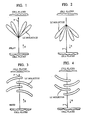
- the flexoelectric effect is exhibited by LC molecules which form structures that have polar symmetry; for example, geometric configurations characterized by splay (FIGS. 1-2) and/or bend (FIGS. 3-4) deformations.
- the effect has two forms, similar to the piezoelectric effect. Either an electric polarization P induces splay or bend curvature, or, vice versa, the curvature induces an electric polarization.
- This invention relates to the first form; an applied electric field E induces polarization P which in turn induces curvature (FIGS. 1-4). Reversing the sign of the electric field likewise reverses the direction of P and of the curvature (FIG. 1 vs.FIG. 2; FIG. 3 vs. FIG. 4) since the two are related in a polar fashion.
- An applied electric field also induces parallel molecular alignment due to the coupling to the dielectric anisotropy. If the dielectric anisotropy is too large, the flexoelectric effect induced by an applied electric field may not be observed.
- the continuously rotating director pattern would have to be formed by the generation of a periodic array of disclination line defects near the electrode surfaces and at the centers of the splay bands.
- these defects would occur most easily with high static fields which undesirably may induce electrohydrodynamic instabilities that tend to obscure the splay-bend structure.
- the flexoelectric effect can be induced in LC materials having chiral centers (e.g. cholesterics, chiral nematics) by causing the helix axis of the LC material to align itself substantially parallel to the plates of a cell incorporating the material.
- An electric field, applied perpendicular to the plates, causes the planes of the directors to rotate about the field direction to an acute angle ⁇ with respect to the helix axis, thereby inducing alternating (e.g. periodic) bands of splay and bend in the material.
- the magnitude of the applied field is maintained low enough that the coupling to the dielectric anisotropy does not unwind the cholesteric helix and cause the molecules to line up with the field.
- periodic disclinations are inherently formed at locations which are near the surface of the plates and where the directors in the bulk are orthogonal to those at the surfaces.
- the relatively high fields of Meyer, supra are not required. Instead, operation at much lower fields is achieved because the field needs only to deform the molecular structure to produce splay and bend.
- the flexoelectric effect may be induced in LC materials by applying a substantially uniform field across the plates and by providing suitable aligning layers on the plates which induce alternating (e.g. periodic) bands of splay and bend in the LC material.
- the ability to rotate the directors of the molecules means that the optical properties of the material can be changed.
- the invention may find use in a number of applications including, for example, optical modulators, optical gratings, or liquid crystal displays.
- FIGS. 7-11 show ideal periodic ordering of the molecules. In reality, however, such ideality is not observed. Thus, within each x-y plane, for example, the directors exhibit orientational order but not positional order.
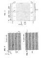
- FIGS. 5-6 there is shown a schematic, isometric view of a portion of a liquid crystal (LC) device.
- the cell includes confinement means such as a pair of substantially parallel plates 13 and 20 which bound, for example, a cholesteric or chiral nematic LC material 30 therebetween.
- the molecules 15 (FIG. 6) of the material are chiral, and arranged in a helical fashion with the helix axis substantially parallel to the plates.
- the LC material may include a single constituent or a plurality of such constituents, one or more of which should be chiral in symmetry.
- the plates 13 and 20, which are transparent to light, have interior major surfaces on which are deposited electrodes 12 and 22.
- Electrodes 40 and 50 are connected to the electrodes to generate a substantially uniform AC electric field E across the LC material and substantially perpendicular to the plates.
- the electrodes may be single broad area layers (e.g. in optical modulators) or an array of stripes (e.g. in a multiplexed display).
- an arrangement for matrix addressing or multiplexing may be provided in which the electrodes are patterned to form arrays of closely spaced stripes, with the two arrays being oriented transverse (e.g. perpendicular) to one another.
- the LC volume in the region of overlap of each pair of stripes defines a picture element (pel).
- the LC material exhibits no switching threshold; so to be effective in providing contrast the cell could incorporate a well-known nonlinear component (e.g. a thin-film transistor (TFT) or metal-insulator-metal (MIM) device) in series with each pel.
- TFT thin-film transistor
- MIM metal-insulator-metal
- the individual pels are selectively addressed by means of suitable electronic switching circuitry incorporated into sources 40 and 50. For simplicity, only two connections to each array are shown.
- the sources 40 and 50 apply suitable voltages across selected electrodes, thereby applying an electric field E across a preselected pel.
- Means for providing optical contrast of light 65 transmitted into and out of the cell illustratively includes polarizers 60 and 70 formed on the glass plates 13 and 20.
- the polarizers may be oriented parallel or at an angle to one another depending on the application.
- the cell When used in the common reflection mode, the cell is also provided with a reflector (not shown) which reflects light transmitted through the cell for retransmission out of the viewing surface.
- a reflector not shown
- the cell is illustratively provided with a pair of aligning layers 80 and 90 on the interior surfaces of the cell.
- Alignment can be effected using the surface treatment described by J.S. Patel et al in Ferroelectrics , Vol. 59, p.129 (1984) and, for example, by cooling the LC material from an isotropic phase to a cholesteric phase in the presence of an electric field.
- these aligning layers cover at least the electrodes in the regions where the electric field is applied to the LC material.
- the layers 80 and 90 cover the electrodes 12 and 22 as well as the interstitial spaces therebetween.
- the LC molecules form a helix (FIGS. 6-9) in which the helix axis is essentially parallel to the plates.
- the directors n of the molecules are oriented substantially perpendicular to the helix axis.
- the planes of the directors rotate about the field direction by an angle ⁇ to the helix axis, and, conversely, in the presence of a negative field (E ⁇ 0; FIG. 9) of the same magnitude the directors rotate by an angle - ⁇ to the helix axis.
- the magnitude of the field is chosen to be low enough that any coupling to the dielectric anisotropy of the LC material does not cause unwinding of the cholesteric helix.
- the molecules exhibit deformation characterized by alternating (e.g., periodic) bands of splay and bend as shown in FIGS. 10 and 11.
- This deformation gives rise to a flexoelectric effect in which the magnitude of the electric field is linearly related to tan ⁇ as shown in FIG. 12.
- Disclinations 21 shown in FIGS. 10-11 are inherently formed at locations which are near the surfaces of plates 13 and 20 and where the directors in the bulk of the LC material are orthogonal to those at the surfaces.
- disclination 21 are located near the surfaces of plates 13 and 20 and at the centers of the splay bands.
- the fact that high electric fields are not required to create the disclinations means that the invention can operate using relatively low magnitude fields.
- e s and e b Associated with the alternating bands of splay and bend deformation are separate flexoelectric coefficients, e s and e b , respectively.
- the average of these coefficients is designated e av .
- e s and e b are of the same sign and are relatively large.
- This example describes an experiment in which the flexoelectric effect was observed in a cholesteric LC material comprising S-4-n-nonyloxyphenyl 4-(3 ⁇ ,7 ⁇ -dimethyloctyloxybenzoyloxy)benzoate.
- the LC material was contained in a cell which was approximately 2.75 ⁇ m thick and which had indium-tin oxide electrodes deposited on glass plates and coated with poly-1-4-butyleneterephthalate to produce parallel molecular alignment at the surfaces. Alignment followed the technique described by J. S. Patel et al, supra. Initial alignment of the helix axis parallel to the glass plates was achieved by cooling the sample from the isotropic state (about 130°C) in the presence of an electric field.
- this orientation of the helix had the lowest dielectric energy.
- the cell was placed between crossed polarizers and aligned for extinction in the absence of an electric field. Measurements of the effect were then made by applying a 40 Hz square wave of variable amplitude across the electrodes and by monitoring the transmitted light intensity with a photodiode and an oscilloscope. For each field amplitude the cell was rotated clockwise and counterclockwise to find the extinction angles for each polarity of field. The dependence of rotation angle on field was found to be linear (FIG. 12) up to the field at which the dielectric coupling resulted in unwinding the helix.
- Example II Using the same alignment procedures as in Example I, but a cell thickness of 2.0 ⁇ m, the flexoelectric effect as described above was observed in a mixture of 0.264 gm of a nematic LC material designated 2141-100 (EM Chemicals, Hawthorne, N.Y.; E. Merck, Darmstadt, W. Germany) and 0.0713 gm of cholesteryl nonanoate.
- 2141-100 EM Chemicals, Hawthorne, N.Y.; E. Merck, Darmstadt, W. Germany
- Example II In an effort to attain an LC material with a tighter pitch, Example II was repeated using 0.2746 gm of the nematic LC 2141-100 and 0.09819 gm of cholesteryl nonanoate. Again, the above flexoelectric effect was observed.
- alternating bands of splay and bend may be induced in LC material by applying a substantially uniform field across the plates and by providing the surface of at least one of the plates with aligning layers comprising periodic zones (e.g., stripes) of substantially homogenous and substantially homeotropic material.
- periodic zones e.g., stripes
- the period of the zones should be substantially equal to the pitch of the helix.
Landscapes
- Physics & Mathematics (AREA)
- Nonlinear Science (AREA)
- Chemical & Material Sciences (AREA)
- Crystallography & Structural Chemistry (AREA)
- General Physics & Mathematics (AREA)
- Optics & Photonics (AREA)
- Liquid Crystal (AREA)
Abstract
Description
- This invention relates to liquid crystal (LC) devices and, more particularly, to such devices which exhibit the flexoelectric effect.
- The flexoelectric effect is exhibited by LC molecules which form structures that have polar symmetry; for example, geometric configurations characterized by splay (FIGS. 1-2) and/or bend (FIGS. 3-4) deformations. The effect has two forms, similar to the piezoelectric effect. Either an electric polarization
P induces splay or bend curvature, or, vice versa, the curvature induces an electric polarization. This invention relates to the first form; an applied electric fieldE induces polarizationP which in turn induces curvature (FIGS. 1-4). Reversing the sign of the electric field likewise reverses the direction ofP and of the curvature (FIG. 1 vs.FIG. 2; FIG. 3 vs. FIG. 4) since the two are related in a polar fashion. - An applied electric field also induces parallel molecular alignment due to the coupling to the dielectric anisotropy. If the dielectric anisotropy is too large, the flexoelectric effect induced by an applied electric field may not be observed.
- The first proposal of the flexoelectric effect was made by R. B. Meyer in Phy. Rev. Lett., Vol. 22, p. 918 (1969). In an ordinary nematic LC material, which is initially uniformly aligned, he proposed that a uniform electric field would induce the formation of a continuously rotating (not in time, but in space) director structure having alternating bands of splay and bend deformation of the type shown in FIG. 2 of the article. However, the formation of such a structure from a uniformly aligned nematic has never been observed for two reasons. First, the flexoelectric effect must compete with ordinary dielectric anisotropy, and the latter coupling usually dominates, maintaining uniform orientation (i.e., molecules lined up with
E ). Second, the continuously rotating director pattern would have to be formed by the generation of a periodic array of disclination line defects near the electrode surfaces and at the centers of the splay bands. However, these defects would occur most easily with high static fields which undesirably may induce electrohydrodynamic instabilities that tend to obscure the splay-bend structure. - On the other hand, the only proposal of the flexoelectric effect in cholesteric or chiral nematic LC materials is found in U.S. Patent No. 4,564,266 granted to G. E. A. Durand on January 14, 1986. However, in Durand the molecules are oriented so that the helix axis is perpendicular to the plates, rather than parallel thereto. In addition, Durand's LC material does not contain periodic bands of splay and bend.
- In accordance with one aspect of the invention, it has been found that the flexoelectric effect can be induced in LC materials having chiral centers (e.g. cholesterics, chiral nematics) by causing the helix axis of the LC material to align itself substantially parallel to the plates of a cell incorporating the material. An electric field, applied perpendicular to the plates, causes the planes of the directors to rotate about the field direction to an acute angle φ with respect to the helix axis, thereby inducing alternating (e.g. periodic) bands of splay and bend in the material. The magnitude of the applied field is maintained low enough that the coupling to the dielectric anisotropy does not unwind the cholesteric helix and cause the molecules to line up with the field.
- Advantageously, in the invention periodic disclinations are inherently formed at locations which are near the surface of the plates and where the directors in the bulk are orthogonal to those at the surfaces. Thus, the relatively high fields of Meyer, supra, are not required. Instead, operation at much lower fields is achieved because the field needs only to deform the molecular structure to produce splay and bend.
- In accordance with another aspect of the invention, the flexoelectric effect may be induced in LC materials by applying a substantially uniform field across the plates and by providing suitable aligning layers on the plates which induce alternating (e.g. periodic) bands of splay and bend in the LC material.
- In either case, the ability to rotate the directors of the molecules means that the optical properties of the material can be changed. Thus, the invention may find use in a number of applications including, for example, optical modulators, optical gratings, or liquid crystal displays.
- The invention, together with is various features and advantages, can be readily understood from the following more detailed description taken in conjunction with accompanying drawing, in which:
- FIGS. 1-2 are schematic representations of LC molecules which exhibit a deformation known as splay;
- FIGS. 3-4 are schematic representations of LC molecules which exhibit a deformation known as bend;
- FIG. 5 is a schematic, isometric view of a LC device;
- FIG. 6 is a schematic, isometric view of the salient features of a flexoelectric LC device in accordance with one embodiment of the invention;
- FIGS. 7-9 are schematic top views of LC molecules in which the directors rotate in space along a helix whose axis is substantially parallel to the plates of cell; in FIGS. 7 and 9 an electric field perpendicular to the plates causes the plane of the directors to rotate to an orientation which is at an angle ±φ to the helix axis depending on the polarity of
E across the plates; in FIG. 8, E = 0 and the directors are perpendicular to the helix axis; and - FIGS. 10 and 11 are cross sections along lines 10-10 and 11-11 of FIGS. 7 and 9, respectively.
- For simplicity of illustrations, FIGS. 7-11 show ideal periodic ordering of the molecules. In reality, however, such ideality is not observed. Thus, within each x-y plane, for example, the directors exhibit orientational order but not positional order.
- With reference now to FIGS. 5-6, there is shown a schematic, isometric view of a portion of a liquid crystal (LC) device. The cell includes confinement means such as a pair of substantially
parallel plates nematic LC material 30 therebetween. In one embodiment the molecules 15 (FIG. 6) of the material are chiral, and arranged in a helical fashion with the helix axis substantially parallel to the plates. The LC material may include a single constituent or a plurality of such constituents, one or more of which should be chiral in symmetry. Theplates electrodes Voltage sources E across the LC material and substantially perpendicular to the plates. Depending on the application, the electrodes may be single broad area layers (e.g. in optical modulators) or an array of stripes (e.g. in a multiplexed display). - If the device is used as a display, an arrangement for matrix addressing or multiplexing may be provided in which the electrodes are patterned to form arrays of closely spaced stripes, with the two arrays being oriented transverse (e.g. perpendicular) to one another. Thus, the LC volume in the region of overlap of each pair of stripes defines a picture element (pel). However, because the flexoelectric effect is linear, the LC material exhibits no switching threshold; so to be effective in providing contrast the cell could incorporate a well-known nonlinear component (e.g. a thin-film transistor (TFT) or metal-insulator-metal (MIM) device) in series with each pel.
- The individual pels are selectively addressed by means of suitable electronic switching circuitry incorporated into
sources sources E across a preselected pel. - Means for providing optical contrast of
light 65 transmitted into and out of the cell illustratively includespolarizers glass plates - When used in the common reflection mode, the cell is also provided with a reflector (not shown) which reflects light transmitted through the cell for retransmission out of the viewing surface.
- In order to align the molecules of the
LC material 30 so that the helix axis is essentially parallel to the plates, the cell is illustratively provided with a pair ofaligning layers layers electrodes - In accordance with one aspect of the invention, the LC molecules form a helix (FIGS. 6-9) in which the helix axis is essentially parallel to the plates. In the absence of an electric field (E = 0; FIG. 8) the directors
n of the molecules are oriented substantially perpendicular to the helix axis. However, in the presence of a positive field (E>0; FIG.7) applied substantially perpendicular to the plates, the planes of the directors rotate about the field direction by an angle φ to the helix axis, and, conversely, in the presence of a negative field (E<0; FIG. 9) of the same magnitude the directors rotate by an angle -φ to the helix axis. - The magnitude of the field is chosen to be low enough that any coupling to the dielectric anisotropy of the LC material does not cause unwinding of the cholesteric helix. Under these circumstances, the molecules exhibit deformation characterized by alternating (e.g., periodic) bands of splay and bend as shown in FIGS. 10 and 11. These figures are cross sections taken along lines 10-10 and 11-11 of FIGS. 7 and 9, respectively; that is, cross sections formed by planes perpendicular to the plane of the helix and at ±φ to the y-axis (director orientation at E = 0). This deformation gives rise to a flexoelectric effect in which the magnitude of the electric field is linearly related to tan φ as shown in FIG. 12.
-
Disclinations 21 shown in FIGS. 10-11 are inherently formed at locations which are near the surfaces ofplates disclination 21 are located near the surfaces ofplates - Associated with the alternating bands of splay and bend deformation are separate flexoelectric coefficients, es and eb, respectively. The average of these coefficients is designated eav. In order to increase the flexoelectric effect it is desirable to utilize materials in which es and ebare of the same sign and are relatively large. In this regard, the effect is also increased in materials in which the pitch po at E = 0 of the helix is larger, as long as the helical structure remains. That is, to a first order approximation, tan φ = eavpoE/2πK, where K is a constant related to the splay, twist and bend elastic constants, K₁,K₂, and K₃ respectively. However, a trade off occurs in that a smaller po may be desirable in some applications (e.g., in a display or an optical grating).
- This example describes an experiment in which the flexoelectric effect was observed in a cholesteric LC material comprising S-4-n-nonyloxyphenyl 4-(3ʹ,7ʹ-dimethyloctyloxybenzoyloxy)benzoate. The LC material was contained in a cell which was approximately 2.75 µm thick and which had indium-tin oxide electrodes deposited on glass plates and coated with poly-1-4-butyleneterephthalate to produce parallel molecular alignment at the surfaces. Alignment followed the technique described by J. S. Patel et al, supra. Initial alignment of the helix axis parallel to the glass plates was achieved by cooling the sample from the isotropic state (about 130°C) in the presence of an electric field. Because this material has a positive dielectric anisotropy, this orientation of the helix had the lowest dielectric energy. The cell was placed between crossed polarizers and aligned for extinction in the absence of an electric field. Measurements of the effect were then made by applying a 40 Hz square wave of variable amplitude across the electrodes and by monitoring the transmitted light intensity with a photodiode and an oscilloscope. For each field amplitude the cell was rotated clockwise and counterclockwise to find the extinction angles for each polarity of field. The dependence of rotation angle on field was found to be linear (FIG. 12) up to the field at which the dielectric coupling resulted in unwinding the helix. Using the equation for tan φ given earlier and the value of the slope in FIG. 12, it was found that eav= 3 x 10⁻⁵cgs units, using K = 1 x 10⁻⁶ dynes and a helix pitch po = 0.5µm.
- Using the same alignment procedures as in Example I, but a cell thickness of 2.0µm, the flexoelectric effect as described above was observed in a mixture of 0.264 gm of a nematic LC material designated 2141-100 (EM Chemicals, Hawthorne, N.Y.; E. Merck, Darmstadt, W. Germany) and 0.0713 gm of cholesteryl nonanoate.
- In an effort to attain an LC material with a tighter pitch, Example II was repeated using 0.2746 gm of the nematic LC 2141-100 and 0.09819 gm of cholesteryl nonanoate. Again, the above flexoelectric effect was observed.
- The above flexoelectric effect was also observed in a mixture of 0.152 gm of a nematic LC material designated K15 (EM Chemicals and E. Merck companies, supra) and 0.025 gm of cholesteryl nonanoate.
- It is to be understood that the above-described arrangements are merely illustrative of the many possible specific embodiments which can be devised to represent application of the principles of the invention. Numerous and varied other arrangements can be devised in accordance with these principles by those skilled in the art without departing from the spirit and scope of the invention. In particular, alternating bands of splay and bend may be induced in LC material by applying a substantially uniform field across the plates and by providing the surface of at least one of the plates with aligning layers comprising periodic zones (e.g., stripes) of substantially homogenous and substantially homeotropic material. When the LC material has a helical structure, the period of the zones should be substantially equal to the pitch of the helix.
Claims (6)
Applications Claiming Priority (3)
| Application Number | Priority Date | Filing Date | Title |
|---|---|---|---|
| US07/022,736 US4917475A (en) | 1987-03-06 | 1987-03-06 | Flexoelectric liquid crystal device |
| US22736 | 1987-03-06 | ||
| SG154794A SG154794G (en) | 1987-03-06 | 1994-10-21 | Flexoelectric liquid cristal device |
Publications (3)
| Publication Number | Publication Date |
|---|---|
| EP0281341A2 true EP0281341A2 (en) | 1988-09-07 |
| EP0281341A3 EP0281341A3 (en) | 1990-05-30 |
| EP0281341B1 EP0281341B1 (en) | 1994-08-24 |
Family
ID=26664457
Family Applications (1)
| Application Number | Title | Priority Date | Filing Date |
|---|---|---|---|
| EP88301724A Expired - Lifetime EP0281341B1 (en) | 1987-03-06 | 1988-02-29 | Flexoelectric liquid cristal device |
Country Status (7)
| Country | Link |
|---|---|
| US (1) | US4917475A (en) |
| EP (1) | EP0281341B1 (en) |
| JP (1) | JPH0797192B2 (en) |
| CA (1) | CA1304492C (en) |
| DE (1) | DE3851166T2 (en) |
| ES (1) | ES2059502T3 (en) |
| SG (1) | SG154794G (en) |
Cited By (7)
| Publication number | Priority date | Publication date | Assignee | Title |
|---|---|---|---|---|
| FR2663770A1 (en) * | 1990-06-22 | 1991-12-27 | Centre Nat Rech Scient | Nematic liquid-crystal display, with surface bistability, controlled by flexoelectric effect |
| WO1992000546A3 (en) * | 1990-06-22 | 1992-02-06 | Centre Nat Rech Scient | Nematic liquid crystal display, having surface bistability and controlled by a flexoelectrical effect |
| EP1408098A1 (en) * | 2002-10-08 | 2004-04-14 | MERCK PATENT GmbH | Liquid crystalline medium and liquid crystal display |
| EP1477547A1 (en) * | 2003-05-09 | 2004-11-17 | MERCK PATENT GmbH | Liquid crystalline medium and liquid crystal display |
| WO2006003441A1 (en) * | 2004-07-02 | 2006-01-12 | Cambridge Enterprise Limited | Flexoelectro-optic liquid crystal device |
| CN102417157A (en) * | 2011-09-21 | 2012-04-18 | 河南工业大学 | Liquid crystal microfluidic drive and control method for MEMS |
| CN108548097A (en) * | 2018-05-10 | 2018-09-18 | 西安交通大学 | There is the transmission pipeline of self-checking function based on the electric principle of flexure |
Families Citing this family (17)
| Publication number | Priority date | Publication date | Assignee | Title |
|---|---|---|---|---|
| US5676880A (en) * | 1987-09-18 | 1997-10-14 | Rolic Ag | Ferroelectric liquid crystal cell |
| EP0309774B1 (en) * | 1987-09-18 | 1992-11-19 | F. Hoffmann-La Roche Ag | Ferroelectric liquid-crystal cell |
| US5247379A (en) * | 1989-02-16 | 1993-09-21 | S. T. Lagerwall S.A.R.L. | Chiral nematic liquid crystal device with linear electroclinic effect |
| US5847790A (en) * | 1989-02-16 | 1998-12-08 | S.T. Lagerwall S.A.R.L. | Liquid crystal devices using a linear electro-optic effect |
| US5040876A (en) * | 1990-03-07 | 1991-08-20 | Bell Communications Research, Inc. | Liquid crystal light modulators with asymmetrical interfaces |
| US5781262A (en) * | 1994-04-19 | 1998-07-14 | Nec Corporation | Liquid crystal display cell |
| US5543950A (en) * | 1995-05-04 | 1996-08-06 | Kent State University | Liquid crystalline electrooptical device |
| JP3465776B2 (en) * | 1996-10-04 | 2003-11-10 | シャープ株式会社 | Liquid crystal display |
| JP2002357851A (en) * | 2001-03-30 | 2002-12-13 | Minolta Co Ltd | Liquid crystal display device |
| ATE314446T1 (en) * | 2002-10-08 | 2006-01-15 | Merck Patent Gmbh | LIQUID CRYSTAL MEDIUM AND LIQUID CRYSTAL DISPLAY |
| US7499125B2 (en) * | 2004-01-28 | 2009-03-03 | Kent State University | Method of fabricating electro-optical devices with polymer-stabilized liquid crystal molecules |
| US7038743B2 (en) * | 2004-01-28 | 2006-05-02 | Kent State University | Electro-optical devices from polymer-stabilized liquid crystal molecules |
| TWI277814B (en) * | 2004-09-23 | 2007-04-01 | Hannstar Display Corp | Flexoelectric liquid crystal display |
| US7652731B2 (en) * | 2006-05-16 | 2010-01-26 | Kent State University | Polymer enhanced cholesteric electro-optical devices |
| GB0906377D0 (en) * | 2009-04-14 | 2009-05-20 | Cambridge Entpr Ltd | Phase modulation devices for optical applications |
| KR102276994B1 (en) | 2014-11-20 | 2021-07-13 | 삼성디스플레이 주식회사 | Liquid crystal display and method of manufacturing the same |
| US10890823B1 (en) * | 2019-10-18 | 2021-01-12 | Facebook Technologies, Llc | Pitch variable optical devices and systems containing the same |
Family Cites Families (7)
| Publication number | Priority date | Publication date | Assignee | Title |
|---|---|---|---|---|
| US3703331A (en) * | 1971-11-26 | 1972-11-21 | Rca Corp | Liquid crystal display element having storage |
| JPS54134452A (en) * | 1978-04-10 | 1979-10-18 | Hitachi Ltd | Quest-host type liquid crystal display device |
| US4333708A (en) * | 1979-11-30 | 1982-06-08 | Bell Telephone Laboratories, Incorporated | Mechanically multistable liquid crystal cell |
| JPS58173718A (en) * | 1982-04-07 | 1983-10-12 | Hitachi Ltd | Liquid crystal light modulator and its manufacturing method |
| FR2526177A1 (en) * | 1982-04-28 | 1983-11-04 | Centre Nat Rech Scient | IMPROVEMENTS TO OPTICAL CELLS USING LIQUID CRYSTALS |
| US4664480A (en) * | 1985-04-26 | 1987-05-12 | American Telephone And Telegraph Company, At&T Bell Laboratories | Alignment technique for liquid crystal devices |
| JPS61264323A (en) * | 1985-05-20 | 1986-11-22 | Fujitsu Ltd | Electrophotographic type liquid crystal printer |
-
1987
- 1987-03-06 US US07/022,736 patent/US4917475A/en not_active Expired - Fee Related
-
1988
- 1988-02-23 CA CA000559604A patent/CA1304492C/en not_active Expired - Lifetime
- 1988-02-29 EP EP88301724A patent/EP0281341B1/en not_active Expired - Lifetime
- 1988-02-29 ES ES88301724T patent/ES2059502T3/en not_active Expired - Lifetime
- 1988-02-29 DE DE3851166T patent/DE3851166T2/en not_active Expired - Fee Related
- 1988-03-01 JP JP63046000A patent/JPH0797192B2/en not_active Expired - Fee Related
-
1994
- 1994-10-21 SG SG154794A patent/SG154794G/en unknown
Cited By (11)
| Publication number | Priority date | Publication date | Assignee | Title |
|---|---|---|---|---|
| FR2663770A1 (en) * | 1990-06-22 | 1991-12-27 | Centre Nat Rech Scient | Nematic liquid-crystal display, with surface bistability, controlled by flexoelectric effect |
| WO1992000546A3 (en) * | 1990-06-22 | 1992-02-06 | Centre Nat Rech Scient | Nematic liquid crystal display, having surface bistability and controlled by a flexoelectrical effect |
| FR2666923A2 (en) * | 1990-06-22 | 1992-03-20 | Centre Nat Rech Scient | Improvements to nematic liquid-crystal displays, with surface bistability, controlled by flexoelectric effect |
| US5357358A (en) * | 1990-06-22 | 1994-10-18 | Centre National De La Recherche Scientifique (Cnrs) | Nematic liquid crystal display with surface bistability and control by flexoelectric effect |
| EP1408098A1 (en) * | 2002-10-08 | 2004-04-14 | MERCK PATENT GmbH | Liquid crystalline medium and liquid crystal display |
| EP1477547A1 (en) * | 2003-05-09 | 2004-11-17 | MERCK PATENT GmbH | Liquid crystalline medium and liquid crystal display |
| WO2006003441A1 (en) * | 2004-07-02 | 2006-01-12 | Cambridge Enterprise Limited | Flexoelectro-optic liquid crystal device |
| CN100489598C (en) * | 2004-07-02 | 2009-05-20 | 剑桥实业有限公司 | Flexoelectro-optic liquid crystal device |
| US8330931B2 (en) | 2004-07-02 | 2012-12-11 | Cambridge Enterprise Limited | Flexoelectro-optic liquid crystal device |
| CN102417157A (en) * | 2011-09-21 | 2012-04-18 | 河南工业大学 | Liquid crystal microfluidic drive and control method for MEMS |
| CN108548097A (en) * | 2018-05-10 | 2018-09-18 | 西安交通大学 | There is the transmission pipeline of self-checking function based on the electric principle of flexure |
Also Published As
| Publication number | Publication date |
|---|---|
| DE3851166D1 (en) | 1994-09-29 |
| EP0281341A3 (en) | 1990-05-30 |
| SG154794G (en) | 1995-03-17 |
| JPH0797192B2 (en) | 1995-10-18 |
| DE3851166T2 (en) | 1994-12-22 |
| CA1304492C (en) | 1992-06-30 |
| ES2059502T3 (en) | 1994-11-16 |
| US4917475A (en) | 1990-04-17 |
| EP0281341B1 (en) | 1994-08-24 |
| JPS63309931A (en) | 1988-12-19 |
Similar Documents
| Publication | Publication Date | Title |
|---|---|---|
| EP0281341B1 (en) | Flexoelectric liquid cristal device | |
| EP0032362B1 (en) | Chiral smectic liquid crystal electro-optical device and process of making the same | |
| US7280175B2 (en) | Liquid crystal device exhibiting zernithal bistability and a cell wall for such a device | |
| US7656490B1 (en) | LC display device with parallel field component | |
| US9280018B2 (en) | Multistable reflective liquid crystal device | |
| JP2548749B2 (en) | Matrix address display | |
| EP1042702B1 (en) | Bistable nematic liquid crystal device | |
| US7876385B2 (en) | Liquid crystal device | |
| JPH09329813A (en) | Electrooptical display device and liquid crystal switching element | |
| WO2008104533A1 (en) | Liquid crystal device | |
| EP0556617A1 (en) | Liquid crystal device and display apparatus | |
| KR100258535B1 (en) | Ferroelectric liquid crystal display device | |
| EP1962131B1 (en) | Liquid crystal device | |
| US5781265A (en) | Non-chiral smectic C liquid crystal display | |
| EP0095012B1 (en) | Liquid crystal display device | |
| US7782438B2 (en) | Fast switching electro-optical devices using banana-shaped liquid crystals | |
| US4799775A (en) | Ferroelectric liquid crystal cells having a helical liquid crystal structure | |
| KR0177975B1 (en) | Twisted Structure Antiferroelectric Liquid Crystal Display | |
| HK79897A (en) | Flexoelectric liquid cristal device | |
| D’havé | Application of antiferroelectric liquid crystals with high tilt | |
| SPLAY | US. Patent Apr. 17, 1990 | |
| WO2003052498A1 (en) | Dual frequency nematic liquid crystal display | |
| US20080106662A1 (en) | Bistable Liquid Crystal Device | |
| EP0271344A2 (en) | Liquid crystal display element and method for driving same | |
| JPH08201774A (en) | Antiferroelectric liquid crystal element |
Legal Events
| Date | Code | Title | Description |
|---|---|---|---|
| PUAI | Public reference made under article 153(3) epc to a published international application that has entered the european phase |
Free format text: ORIGINAL CODE: 0009012 |
|
| AK | Designated contracting states |
Kind code of ref document: A2 Designated state(s): BE CH DE ES FR GB LI NL SE |
|
| PUAL | Search report despatched |
Free format text: ORIGINAL CODE: 0009013 |
|
| AK | Designated contracting states |
Kind code of ref document: A3 Designated state(s): BE CH DE ES FR GB LI NL SE |
|
| 17P | Request for examination filed |
Effective date: 19901123 |
|
| 17Q | First examination report despatched |
Effective date: 19921020 |
|
| RAP3 | Party data changed (applicant data changed or rights of an application transferred) |
Owner name: AT&T CORP. |
|
| GRAA | (expected) grant |
Free format text: ORIGINAL CODE: 0009210 |
|
| AK | Designated contracting states |
Kind code of ref document: B1 Designated state(s): BE CH DE ES FR GB LI NL SE |
|
| REF | Corresponds to: |
Ref document number: 3851166 Country of ref document: DE Date of ref document: 19940929 |
|
| REG | Reference to a national code |
Ref country code: ES Ref legal event code: FG2A Ref document number: 2059502 Country of ref document: ES Kind code of ref document: T3 |
|
| ET | Fr: translation filed | ||
| EAL | Se: european patent in force in sweden |
Ref document number: 88301724.6 |
|
| PLBE | No opposition filed within time limit |
Free format text: ORIGINAL CODE: 0009261 |
|
| STAA | Information on the status of an ep patent application or granted ep patent |
Free format text: STATUS: NO OPPOSITION FILED WITHIN TIME LIMIT |
|
| 26N | No opposition filed | ||
| PGFP | Annual fee paid to national office [announced via postgrant information from national office to epo] |
Ref country code: GB Payment date: 19980109 Year of fee payment: 11 |
|
| PGFP | Annual fee paid to national office [announced via postgrant information from national office to epo] |
Ref country code: SE Payment date: 19980112 Year of fee payment: 11 |
|
| PGFP | Annual fee paid to national office [announced via postgrant information from national office to epo] |
Ref country code: FR Payment date: 19980119 Year of fee payment: 11 |
|
| PGFP | Annual fee paid to national office [announced via postgrant information from national office to epo] |
Ref country code: BE Payment date: 19980127 Year of fee payment: 11 |
|
| PGFP | Annual fee paid to national office [announced via postgrant information from national office to epo] |
Ref country code: DE Payment date: 19980129 Year of fee payment: 11 |
|
| PGFP | Annual fee paid to national office [announced via postgrant information from national office to epo] |
Ref country code: CH Payment date: 19980205 Year of fee payment: 11 |
|
| PGFP | Annual fee paid to national office [announced via postgrant information from national office to epo] |
Ref country code: ES Payment date: 19980217 Year of fee payment: 11 |
|
| PGFP | Annual fee paid to national office [announced via postgrant information from national office to epo] |
Ref country code: NL Payment date: 19980228 Year of fee payment: 11 |
|
| PG25 | Lapsed in a contracting state [announced via postgrant information from national office to epo] |
Ref country code: LI Free format text: LAPSE BECAUSE OF NON-PAYMENT OF DUE FEES Effective date: 19990228 Ref country code: GB Free format text: LAPSE BECAUSE OF NON-PAYMENT OF DUE FEES Effective date: 19990228 Ref country code: CH Free format text: LAPSE BECAUSE OF NON-PAYMENT OF DUE FEES Effective date: 19990228 Ref country code: BE Free format text: LAPSE BECAUSE OF NON-PAYMENT OF DUE FEES Effective date: 19990228 |
|
| PG25 | Lapsed in a contracting state [announced via postgrant information from national office to epo] |
Ref country code: SE Free format text: LAPSE BECAUSE OF NON-PAYMENT OF DUE FEES Effective date: 19990301 Ref country code: ES Free format text: LAPSE BECAUSE OF NON-PAYMENT OF DUE FEES Effective date: 19990301 |
|
| BERE | Be: lapsed |
Owner name: AT&T CORP. Effective date: 19990228 |
|
| PG25 | Lapsed in a contracting state [announced via postgrant information from national office to epo] |
Ref country code: NL Free format text: LAPSE BECAUSE OF NON-PAYMENT OF DUE FEES Effective date: 19990901 |
|
| REG | Reference to a national code |
Ref country code: CH Ref legal event code: PL |
|
| GBPC | Gb: european patent ceased through non-payment of renewal fee |
Effective date: 19990228 |
|
| PG25 | Lapsed in a contracting state [announced via postgrant information from national office to epo] |
Ref country code: FR Free format text: LAPSE BECAUSE OF NON-PAYMENT OF DUE FEES Effective date: 19991029 |
|
| EUG | Se: european patent has lapsed |
Ref document number: 88301724.6 |
|
| PG25 | Lapsed in a contracting state [announced via postgrant information from national office to epo] |
Ref country code: DE Free format text: LAPSE BECAUSE OF NON-PAYMENT OF DUE FEES Effective date: 19991201 |
|
| REG | Reference to a national code |
Ref country code: FR Ref legal event code: ST |
|
| EUG | Se: european patent has lapsed |
Ref document number: 88301724.6 |
|
| REG | Reference to a national code |
Ref country code: ES Ref legal event code: FD2A Effective date: 20010910 |