EP0281303A2 - Modulo-arithmetischer Rechnerchip - Google Patents
Modulo-arithmetischer Rechnerchip Download PDFInfo
- Publication number
- EP0281303A2 EP0281303A2 EP88301541A EP88301541A EP0281303A2 EP 0281303 A2 EP0281303 A2 EP 0281303A2 EP 88301541 A EP88301541 A EP 88301541A EP 88301541 A EP88301541 A EP 88301541A EP 0281303 A2 EP0281303 A2 EP 0281303A2
- Authority
- EP
- European Patent Office
- Prior art keywords
- integer
- bits
- base
- carry
- register
- Prior art date
- Legal status (The legal status is an assumption and is not a legal conclusion. Google has not performed a legal analysis and makes no representation as to the accuracy of the status listed.)
- Withdrawn
Links
Images


Classifications
-
- G—PHYSICS
- G06—COMPUTING; CALCULATING OR COUNTING
- G06F—ELECTRIC DIGITAL DATA PROCESSING
- G06F7/00—Methods or arrangements for processing data by operating upon the order or content of the data handled
- G06F7/60—Methods or arrangements for performing computations using a digital non-denominational number representation, i.e. number representation without radix; Computing devices using combinations of denominational and non-denominational quantity representations, e.g. using difunction pulse trains, STEELE computers, phase computers
- G06F7/72—Methods or arrangements for performing computations using a digital non-denominational number representation, i.e. number representation without radix; Computing devices using combinations of denominational and non-denominational quantity representations, e.g. using difunction pulse trains, STEELE computers, phase computers using residue arithmetic
- G06F7/722—Modular multiplication
-
- G—PHYSICS
- G06—COMPUTING; CALCULATING OR COUNTING
- G06F—ELECTRIC DIGITAL DATA PROCESSING
- G06F2207/00—Indexing scheme relating to methods or arrangements for processing data by operating upon the order or content of the data handled
- G06F2207/38—Indexing scheme relating to groups G06F7/38 - G06F7/575
- G06F2207/3804—Details
- G06F2207/3808—Details concerning the type of numbers or the way they are handled
- G06F2207/3812—Devices capable of handling different types of numbers
- G06F2207/3816—Accepting numbers of variable word length
-
- G—PHYSICS
- G06—COMPUTING; CALCULATING OR COUNTING
- G06F—ELECTRIC DIGITAL DATA PROCESSING
- G06F7/00—Methods or arrangements for processing data by operating upon the order or content of the data handled
- G06F7/60—Methods or arrangements for performing computations using a digital non-denominational number representation, i.e. number representation without radix; Computing devices using combinations of denominational and non-denominational quantity representations, e.g. using difunction pulse trains, STEELE computers, phase computers
- G06F7/72—Methods or arrangements for performing computations using a digital non-denominational number representation, i.e. number representation without radix; Computing devices using combinations of denominational and non-denominational quantity representations, e.g. using difunction pulse trains, STEELE computers, phase computers using residue arithmetic
- G06F7/723—Modular exponentiation
Definitions
- This invention relates to a processor chip and in particular, but not exclusively to a processor chip for computing addition, multiplication, and exponentiation in the Galois Field of integers modulo a prime number.
- the received non-secret transformation of the other converser's secret signal is again transformed with the receiving converser's secret signal to generate a secure cipher key.
- the transformations use known operations that are easily performed but extremely difficult to invert. It is believed infeasible for an eavesdropper to invert the initial non-secret transformation to obtain either converser's secret signal, or duplicate the latter transformation and obtain the secure cipher key.
- Embodiments of the present invention provide a processor chip for computing addition, multiplication, and exponentiation in the Galois Field of integers modulo a prime number p.
- Embodiments of the present invention provide a processor chip for performing an exponentiation operation in a rapid manner.
- an apparatus for computing multiplication in the ring of integers modulo an integer number, p comprising: an X register having L-bits for storing an n-bit integer X; a Y register having L-bits for storing an n-bit integer Y; first and second A registers for storing L-bits each; means for transforming the n-bit integer X from X register into first and second alternate integers having L-bits each and storing first and second alternate integers in said first and second registers A; control means connected to said first and second A registers for generating a control signal; first and second B registers for storing L-bits each; first and second C registers for storing L-bits each; a full adder coupled to said first and second B registers, said first and second V registers, and said control logic, and responsive to the control signal being a 1-bit for shifting left and adding data stored in said first and second B registers to data stored in said first and second C registers
- a processor chip for adding a first integer having n-bits to a second integer having n-bits, wherein the first integer plus the second integer equals a third integer having n-bits, modulo a fourth integer having n-bits, is provided, comprising first register means for storing the first integer, second register means for storing the second integer, and feedback means for generating and storing a feedback number.
- the feedback number is the two's complement of the fourth integer.
- These embodiments include arithmetic means coupled to the first register means and the second register means. The arithmetic means is for adding the first integer to the second integer, thereby generating the third integer.
- the third integer is then stored in accumulator means which is coupled to arithmetic means.
- These embodiments further include overflow means coupled to the accumulator means for storing an overflow integer which is overflowed from the third integer.
- means is provided for fetching the feedback number into the second register and adding the feedback number using arithmetic means to the third integer in the accumulator means.
- means coupled to the accumulator means and responsive to the third integer being greater than the fourth integer may be provided for reducing the third integer modulo the fourth integer.
- a further embodiment of this invention includes a modulo arithmetic processor chip for multiplying a first integer having n-bits by a second integer having n-bits, wherein the first integer times the second integer equals a third integer having n-bits, modulo a fourth integer having n-bits.
- the modulo arithmetic processor chip for multiplying includes first register means for storing the first integer, second register means for storing the second integer, feedback means for generating a feedback number, wherein the feedback number equals the two's complement of the fourth integer, and arithmetic means coupled to the first register means and the second register means, and responsive to the least significant position of the first integer shifted right from the first register means, for adding the second integer to the third integer.
- Accumulator means is provided coupled to the arithmetic means for storing the third integer. Also included is overflow means coupled to the accumulator means for counting and storing overflow bits as an overflow integer and second partial reduction means coupled to the overflow means, the feedback means, the first register means and the second register means, and responsive to the completion of multiplying the first integer by the second integer, for transferring the overflow integer into the first register means, transferring the feedback number into the second register means, and multiplying the feedback number by the overflow integer to generate a product, and adding the product to the third integer in the accumulator register means. Means is provided coupled to the accumulator means and responsive to the third integer being greater than the fourth integer, for reducing the third integer modulo the fourth integer. Also, first partial reduction means is included coupled to the second register means and responsive to the most significant position of the second integer shifted left from the second register means, for adding the feedback number to the second integer, thereby partially reducing the second integer.
- a preferred embodiment of the present invention includes an X register having L-bits storage for storing an N-bit integer X, a Y register having L-bits storage for storing an N-bit register Y, and first and second A registers for storing L-bits each.
- the invention includes means for transforming the N-bit integer X from X register into first and second alternate integers having L-bits each and storing first and second alternate integers in the first and second registers A. Also included are control means connected to the first and second registers for generating control signal.
- First and second B registers for storing L-bits each, and first and second C registers for storing L-bits each are coupled to a full adder.
- the control logic also is coupled to the full adder, and the full adder is responsive to a control signal being a 1-bit from the control logic, for shifting left and adding data stored in the first and second B registers to data stored in the first and second C registers.
- the full adder is responsive to the control logic signal being a 0-bit for shifting left data in the first and second B registers.
- a feedback register having L-bits for storing an N-bit feedback number is included along with means for generating a feedback number from a prime number, p, having N-bits and storing the feedback number in the feedback register.
- Modulo means is coupled to the feedback register and the first and second C register for reducing data bits stored in the first and second C registers modulo the prime number p and means for converting data bits in the first and second C registers to an L-bit integer and storing the L bit integer in the Y register.
- the processor chip computes addition, multiplication, and exponentiation in the Galois Field of integers modulo a prime number p, GF(p).
- GF(p) For large prime numbers, several chips can be cascaded together to function as an equivalent single larger chip. Also these chips can be used for computing exponentiation in the ring of integers modulo a composite number, the factorization of which is kept secret, such as in the RSA public key cryptographic scheme.
- the following discussions focus on the Galois Field GF(p) where p is a prime number.
- p is an n-bit number with the radix-two form (usual binary representation)
- p P[n-1]2 n-1 + P[n-2]2 n-2 +...+ P[1]2 + P[0] where ⁇ P[i] ⁇ are binary symbols.
- p 2 n - F[n-1]2 n-1 - F[n-2]2 n-2 -...- F[1]2-F[0] where ⁇ F[i] ⁇ are binary symbols.
- ⁇ Z[i] ⁇ and ⁇ X[i] ⁇ are binary symbols.
- a partial reduction at each stage can be performed using the relationship in Eq. (1). This partial reduction allows representing all integers by n binary symbols.
- the heart of the processor chip is the GF(p) multiply operation.
- a and B that belong to GF(p). These are any two integers less than p.
- C AB mod p.
- A, B, and C are referred to as the "multiplier,” the “multiplicand,” and the "product,” respectively
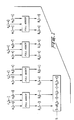
- integers A, B, and C are represented by n 2-bit integer components.
- the control logic for the multiplier is at the right end of the A1 and A2 n-bit registers. It has binary variables r1, r2, and A21 originally set to zero.
- the multiplier logic at the right end of the A1 and A2 registers merely converts the non-unique n-bit radix-two form where the resulting bits ⁇ r ⁇ 1 ⁇ are used to control the adding of the shifted multiplicand registers B1 and B2 to the product accumulator registers C1 and C2.
- the multiplicand is held in two n-bit registers B1 and B2, which are shifted left (multiplied by 2). Before each left shift of the B1 and B2 registers; these register bits are added or not added to the product accumulator registers C1 and C2 depending on the multiplier logic output bit r ⁇ 1.
- the multiplicand B has the form or on rearranging terms, the form Multiplying by 2 gives Recall that each 2 n term can be replaced by the feedback terms using Eq. (1).
- C which consists of two n-bit registers.
- the problem of handling overflow terms must be taken care of using Eq. (1). Since no shifting of the C register is involved, all the overflow terms are accumulated until all shifts and adds are completed. At the end of the shifts and adds, all the accumulated overflow terms are added to the C registers to obtain the final answer.
- each adding of B to C is illustrated in Fig. 2 in terms of two sets of full adders.
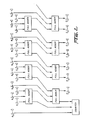
- the contents in the two n-bit registers C1 and C2 can be transferred to the two n-bit registers A1, A2, and/or B1, B2 to continue the exponentiation algorithm.
- Step 1 Set N ⁇ --- n Step : I ⁇ --- 0
- Step 2 Set C ⁇ --- C + 0 N ⁇ --- N - 1
- Step 1 Set Y ⁇ --- C
- Step 2 Set C ⁇ --- C + F1
- Step 3 Set N ⁇ --- n I ⁇ --- 0
- Step 4 Set C ⁇ --- C + 0 N ⁇ --- N - 1
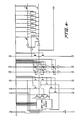
- the processor chip has the basic structure illustrated in Fig. 3, comprising of 12 L-bit registers, L full adders, and control and feedback logic.
- the prime number feedback terms F3 and F4 are computed from input F1 while F2 is merely a shift of F1.
- Other inputs to this chip are the integer X and the integer Z. Assume that all these integers are represented by L bits and that the prime number p is an L-bit integer.
- the final exponentiation will be located in the L-bit registers Y. Anytime after loading the F1, Z, and X registers, a start command can initiate the add, multiply, or exponentiation computation. Loading in these registers is not allowed during computations.
- the bulk of the basic structure consists of the set of 12 L-bit registers and L full adders. A vertical slice through this basic structure, is shown as the basic cell of Fig. 4.
- the bulk of the basic structure of Fig. 3 includes identical copies of the basic cell shown in Fig. 4 that are cascaded L times much like a set of register cells.
- the basic cell consists of 12 registers and single full adder which is time shared to do the operations shown in Figs. 1 and 2. Illustrated in Fig. 4 are load lines and communication lines where a basic cell receives inputs from two right adjacent cells and sends outputs to two left adjacent cells. Also there is a control bit r ⁇ 1 that goes to all cells from right to left and three feedback bits ⁇ 0, ⁇ 1, and ⁇ 3 that goes to all cells from left to right.
- the processor chip includes L basic cells and, therefore, all integers of interest are L-bit integers.
- the prime number p also was assumed to be an L-bit prime integer.
- the integer X is an n-bit integer and the result of addition, multiplication, or exponentiation is also an n-bit integer.
- the n-bit integers X and F are loaded into the highest n-bit register positions of the X and F registers.
- the highest m-bit positions of the Z registers are loaded with the m-bit integer Z. This is shown in Fig. 5.
- a modular design is used where there are L basic cells on a single chip.
- a single chip can compute exponentiation for any n-bit prime number p where n ⁇ L.
- two chips in cascade can act like a single chip with 2L basic cells and handle prime numbers where n ⁇ 2L.
- the modular design is such that K modular chips in cascade behaves like a single chip of KL basic cells that can compute exponentiation in GF(p) where p is an n-bit prime with n ⁇ KL.
- Fig. 3 To achieve this modular design, consider the structure of Fig. 3 to represent a modular chip where the left end logic circuits can be disengaged by an input control pin and the right end logic circuits can be disengaged by another input control pin. Input and output pins are located on each chip to allow two chips to connect together so that the sequence of the basic cells continue from one chip to the next chip. Thus all chips have L basic cells and all the end logic circuits as shown in Fig. 3. The primary modification is that the end logic circuits can be disengaged, and chips can be connected to continue the cascade of basic cells.
- a cascade of K modular chips then has a left most chip with its left logic circuits engaged and its right logic circuits disengaged.
- the K-2 intermediate chips have all end logic circuits disengaged while the right most chip has its left logic circuits disengaged and its right logic circuits engaged. Since the end logic circuits take up only a small fraction of each modular chip, there is little total chip area lost to the unused end logic circuits.
- the overall chip controller that also is duplicated on each chip although only used on the left most chip in a cascade of modular chips. This chip controller, which also takes up little chip area, is described next.
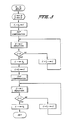
- n the number of bits in the representation of the prime p
- MPY overflow compensation is represented as, OVF Compensation and the two n-bit to one n-bit reduction is represented as,
- the three subroutines are shown in Figures 6, 7, and 8.
- the counter in Fig. 2 has count integer denoted I, which is the overflow index used in these subroutines.
- Multiplication is the most common subroutine used in exponentiation. Overflow compensation is used to check for a 2 n term in the counter (see Fig. 2) and, if so, apply a feedback term using Eq. (1).
- the two n-bit to one n-bit reduction forces n additions of 0 to C.
- Fig. 10 This consists of three separate functions of exponentiation, multiplication, and addition followed by a common part that first reduces the answer in the C1 and C2 registers into a single n-bit form in C1 and then completes the final mod p reduction.
Landscapes
- Physics & Mathematics (AREA)
- Engineering & Computer Science (AREA)
- General Physics & Mathematics (AREA)
- Mathematical Analysis (AREA)
- Mathematical Optimization (AREA)
- Pure & Applied Mathematics (AREA)
- Computational Mathematics (AREA)
- Theoretical Computer Science (AREA)
- Computing Systems (AREA)
- Mathematical Physics (AREA)
- General Engineering & Computer Science (AREA)
- Error Detection And Correction (AREA)
- Detection And Correction Of Errors (AREA)
- Compression, Expansion, Code Conversion, And Decoders (AREA)
Applications Claiming Priority (2)
| Application Number | Priority Date | Filing Date | Title |
|---|---|---|---|
| US2166087A | 1987-03-04 | 1987-03-04 | |
| US21660 | 1987-03-04 |
Publications (2)
| Publication Number | Publication Date |
|---|---|
| EP0281303A2 true EP0281303A2 (de) | 1988-09-07 |
| EP0281303A3 EP0281303A3 (de) | 1990-08-29 |
Family
ID=21805457
Family Applications (1)
| Application Number | Title | Priority Date | Filing Date |
|---|---|---|---|
| EP88301541A Withdrawn EP0281303A3 (de) | 1987-03-04 | 1988-02-23 | Modulo-arithmetischer Rechnerchip |
Country Status (1)
| Country | Link |
|---|---|
| EP (1) | EP0281303A3 (de) |
Cited By (6)
| Publication number | Priority date | Publication date | Assignee | Title |
|---|---|---|---|---|
| EP0566498A2 (de) * | 1992-04-16 | 1993-10-20 | FORTRESS U&T Ltd. | Einrichtung und Verfahren zur digitalen Unterschrift |
| US5513133A (en) * | 1992-11-30 | 1996-04-30 | Fortress U&T Ltd. | Compact microelectronic device for performing modular multiplication and exponentiation over large numbers |
| WO1999030250A1 (fr) | 1997-12-10 | 1999-06-17 | Seiko Epson Corporation | Systeme informatique, systeme cryptographique, circuit systeme lsi, et appareil electronique |
| KR100431576B1 (ko) * | 1995-08-29 | 2004-08-25 | 아트멜 코포레이숀 | 갈로아필드다항식승산/제산회로및그것을통합하는디지탈신호프로세서 |
| US6963977B2 (en) * | 2000-12-19 | 2005-11-08 | International Business Machines Corporation | Circuits and methods for modular exponentiation |
| CN105373366A (zh) * | 2015-10-12 | 2016-03-02 | 武汉瑞纳捷电子技术有限公司 | 一种生成大素数的方法及装置 |
Citations (2)
| Publication number | Priority date | Publication date | Assignee | Title |
|---|---|---|---|---|
| US4405829A (en) * | 1977-12-14 | 1983-09-20 | Massachusetts Institute Of Technology | Cryptographic communications system and method |
| EP0133202A2 (de) * | 1983-06-28 | 1985-02-20 | Siemens Aktiengesellschaft | Verfahren zum Potenzieren in Galois-Feldern GF(2n) für Zwecke der Datenverarbeitung, der Datensicherung, der Datenübertragung usw., insbesondere für den Schlüsselaustausch für eine verschlüsselte Datenübertragung, und Schaltungsanordnung zur Durchführung des Verfahrens |
-
1988
- 1988-02-23 EP EP88301541A patent/EP0281303A3/de not_active Withdrawn
Patent Citations (2)
| Publication number | Priority date | Publication date | Assignee | Title |
|---|---|---|---|---|
| US4405829A (en) * | 1977-12-14 | 1983-09-20 | Massachusetts Institute Of Technology | Cryptographic communications system and method |
| EP0133202A2 (de) * | 1983-06-28 | 1985-02-20 | Siemens Aktiengesellschaft | Verfahren zum Potenzieren in Galois-Feldern GF(2n) für Zwecke der Datenverarbeitung, der Datensicherung, der Datenübertragung usw., insbesondere für den Schlüsselaustausch für eine verschlüsselte Datenübertragung, und Schaltungsanordnung zur Durchführung des Verfahrens |
Non-Patent Citations (2)
| Title |
|---|
| IEEE TRANSACTIONS ON COMPUTERS, vol. C-32, no. 4, April 1983, pages 378-387, IEEE, New York, US; P. KORNERUP et al.: "Finite precision rational arithmetic: An arithmetic unit" * |
| PROCEEDINGS 5TH SYMPOSIUM ON COMPUTER ARITHMETIC, Ann Arbor, Michigan, 18th - 19th May 1981, pages 233-240, IEEE, New York, US; P. KORNERUP et al.: "An integrated rational arithmetic unit" * |
Cited By (9)
| Publication number | Priority date | Publication date | Assignee | Title |
|---|---|---|---|---|
| EP0566498A2 (de) * | 1992-04-16 | 1993-10-20 | FORTRESS U&T Ltd. | Einrichtung und Verfahren zur digitalen Unterschrift |
| EP0566498A3 (en) * | 1992-04-16 | 1994-10-12 | Fortress U & T Ltd | Digital signature device and process |
| US5448639A (en) * | 1992-04-16 | 1995-09-05 | Fortress U&T Ltd. | Digital signature device |
| US5513133A (en) * | 1992-11-30 | 1996-04-30 | Fortress U&T Ltd. | Compact microelectronic device for performing modular multiplication and exponentiation over large numbers |
| US5742530A (en) * | 1992-11-30 | 1998-04-21 | Fortress U&T Ltd. | Compact microelectronic device for performing modular multiplication and exponentiation over large numbers |
| KR100431576B1 (ko) * | 1995-08-29 | 2004-08-25 | 아트멜 코포레이숀 | 갈로아필드다항식승산/제산회로및그것을통합하는디지탈신호프로세서 |
| WO1999030250A1 (fr) | 1997-12-10 | 1999-06-17 | Seiko Epson Corporation | Systeme informatique, systeme cryptographique, circuit systeme lsi, et appareil electronique |
| US6963977B2 (en) * | 2000-12-19 | 2005-11-08 | International Business Machines Corporation | Circuits and methods for modular exponentiation |
| CN105373366A (zh) * | 2015-10-12 | 2016-03-02 | 武汉瑞纳捷电子技术有限公司 | 一种生成大素数的方法及装置 |
Also Published As
| Publication number | Publication date |
|---|---|
| EP0281303A3 (de) | 1990-08-29 |
Similar Documents
| Publication | Publication Date | Title |
|---|---|---|
| US4891781A (en) | Modulo arithmetic processor chip | |
| US5210710A (en) | Modulo arithmetic processor chip | |
| US5289397A (en) | High-speed modulo exponentiator device | |
| US4994997A (en) | Pipeline-type serial multiplier circuit | |
| US5448639A (en) | Digital signature device | |
| JP3784156B2 (ja) | モジュラ掛け算方法 | |
| US6049815A (en) | Method and apparatus for finite field multiplication | |
| US6397241B1 (en) | Multiplier cell and method of computing | |
| KR100591761B1 (ko) | 몽고메리 모듈러 곱셈기 및 캐리 저장 가산을 이용한몽고메리 모듈러 곱셈 방법 | |
| EP0801345A1 (de) | Schaltung und Verfahren für Modulo-Multiplikations- und Exponentiationsarithmetik | |
| JP4554239B2 (ja) | モンゴメリー類型のモジュラー乗算装置及び方法 | |
| EP1471420A2 (de) | Modularer Montgomery Multiplizierer und Verfahren dafür mit "carry-save" Addition | |
| US5261001A (en) | Microcircuit for the implementation of RSA algorithm and ordinary and modular arithmetic, in particular exponentiation, with large operands | |
| JPH08263316A (ja) | モンゴメリ法によるモジュラ乗算の実施方法 | |
| US7480691B2 (en) | Arithmetic device for multiple precision arithmetic for Montgomery multiplication residue arithmetic | |
| EP0281303A2 (de) | Modulo-arithmetischer Rechnerchip | |
| JP3302043B2 (ja) | 暗号通信方法及びそのシステム | |
| US20010054053A1 (en) | Method and apparatus for finite field multiplication | |
| US7607165B2 (en) | Method and apparatus for multiplication and/or modular reduction processing | |
| KR100480997B1 (ko) | GF(p)와 GF(2^m)의 유한체 곱셈 연산 장치 | |
| CN115268839A (zh) | 一种以2为基的蒙哥马利模乘方法及装置 | |
| US5258945A (en) | Method and apparatus for generating multiples of BCD number | |
| Lu et al. | A programmable VLSI architecture for computing multiplication and polynomial evaluation modulo a positive integer | |
| EP0353041A2 (de) | Gerät und Verfahren zur Verarbeitung von Signalen mit Hilfe von modifizierter Vorzeichenziffernarithmetik | |
| KR20040045152A (ko) | 모듈러 곱셈 장치 |
Legal Events
| Date | Code | Title | Description |
|---|---|---|---|
| PUAI | Public reference made under article 153(3) epc to a published international application that has entered the european phase |
Free format text: ORIGINAL CODE: 0009012 |
|
| AK | Designated contracting states |
Kind code of ref document: A2 Designated state(s): CH DE FR GB LI |
|
| PUAL | Search report despatched |
Free format text: ORIGINAL CODE: 0009013 |
|
| AK | Designated contracting states |
Kind code of ref document: A3 Designated state(s): CH DE FR GB LI |
|
| 17P | Request for examination filed |
Effective date: 19910207 |
|
| STAA | Information on the status of an ep patent application or granted ep patent |
Free format text: STATUS: THE APPLICATION IS DEEMED TO BE WITHDRAWN |
|
| 18D | Application deemed to be withdrawn |
Effective date: 19930901 |