EP0281011B1 - Edge-illuminated impurity band conduction detector arrays - Google Patents
Edge-illuminated impurity band conduction detector arrays Download PDFInfo
- Publication number
- EP0281011B1 EP0281011B1 EP88102761A EP88102761A EP0281011B1 EP 0281011 B1 EP0281011 B1 EP 0281011B1 EP 88102761 A EP88102761 A EP 88102761A EP 88102761 A EP88102761 A EP 88102761A EP 0281011 B1 EP0281011 B1 EP 0281011B1
- Authority
- EP
- European Patent Office
- Prior art keywords
- detector
- conductivity type
- focal plane
- detectors
- optical
- Prior art date
- Legal status (The legal status is an assumption and is not a legal conclusion. Google has not performed a legal analysis and makes no representation as to the accuracy of the status listed.)
- Expired - Lifetime
Links
- 239000012535 impurity Substances 0.000 title claims description 46
- 238000003491 array Methods 0.000 title claims description 16
- 230000003287 optical effect Effects 0.000 claims description 38
- 230000003595 spectral effect Effects 0.000 claims description 16
- 230000000903 blocking effect Effects 0.000 claims description 13
- 239000000758 substrate Substances 0.000 claims description 8
- 239000000969 carrier Substances 0.000 claims description 7
- 230000007246 mechanism Effects 0.000 claims description 6
- 230000005540 biological transmission Effects 0.000 claims description 5
- 230000005684 electric field Effects 0.000 claims 6
- 239000000463 material Substances 0.000 description 7
- 230000004044 response Effects 0.000 description 6
- 238000001514 detection method Methods 0.000 description 5
- 239000007787 solid Substances 0.000 description 4
- XUIMIQQOPSSXEZ-UHFFFAOYSA-N Silicon Chemical compound [Si] XUIMIQQOPSSXEZ-UHFFFAOYSA-N 0.000 description 3
- 238000010521 absorption reaction Methods 0.000 description 3
- 229910052710 silicon Inorganic materials 0.000 description 3
- 239000010703 silicon Substances 0.000 description 3
- 238000004458 analytical method Methods 0.000 description 2
- 229910052785 arsenic Inorganic materials 0.000 description 2
- RQNWIZPPADIBDY-UHFFFAOYSA-N arsenic atom Chemical compound [As] RQNWIZPPADIBDY-UHFFFAOYSA-N 0.000 description 2
- 230000008859 change Effects 0.000 description 2
- 238000003384 imaging method Methods 0.000 description 2
- 230000003993 interaction Effects 0.000 description 2
- 239000004065 semiconductor Substances 0.000 description 2
- 238000001228 spectrum Methods 0.000 description 2
- 238000000862 absorption spectrum Methods 0.000 description 1
- 239000013078 crystal Substances 0.000 description 1
- 239000002019 doping agent Substances 0.000 description 1
- 230000005670 electromagnetic radiation Effects 0.000 description 1
- 230000004907 flux Effects 0.000 description 1
- 238000005286 illumination Methods 0.000 description 1
- 238000004519 manufacturing process Methods 0.000 description 1
- 238000000034 method Methods 0.000 description 1
- 238000012986 modification Methods 0.000 description 1
- 230000004048 modification Effects 0.000 description 1
- 238000000255 optical extinction spectrum Methods 0.000 description 1
- 230000005855 radiation Effects 0.000 description 1
- 239000012780 transparent material Substances 0.000 description 1
Images


Classifications
-
- H—ELECTRICITY
- H01—ELECTRIC ELEMENTS
- H01L—SEMICONDUCTOR DEVICES NOT COVERED BY CLASS H10
- H01L27/00—Devices consisting of a plurality of semiconductor or other solid-state components formed in or on a common substrate
- H01L27/14—Devices consisting of a plurality of semiconductor or other solid-state components formed in or on a common substrate including semiconductor components sensitive to infrared radiation, light, electromagnetic radiation of shorter wavelength or corpuscular radiation and specially adapted either for the conversion of the energy of such radiation into electrical energy or for the control of electrical energy by such radiation
- H01L27/144—Devices controlled by radiation
- H01L27/146—Imager structures
- H01L27/14643—Photodiode arrays; MOS imagers
- H01L27/14645—Colour imagers
-
- G—PHYSICS
- G01—MEASURING; TESTING
- G01J—MEASUREMENT OF INTENSITY, VELOCITY, SPECTRAL CONTENT, POLARISATION, PHASE OR PULSE CHARACTERISTICS OF INFRARED, VISIBLE OR ULTRAVIOLET LIGHT; COLORIMETRY; RADIATION PYROMETRY
- G01J3/00—Spectrometry; Spectrophotometry; Monochromators; Measuring colours
- G01J3/02—Details
- G01J3/0256—Compact construction
- G01J3/0259—Monolithic
-
- G—PHYSICS
- G01—MEASURING; TESTING
- G01J—MEASUREMENT OF INTENSITY, VELOCITY, SPECTRAL CONTENT, POLARISATION, PHASE OR PULSE CHARACTERISTICS OF INFRARED, VISIBLE OR ULTRAVIOLET LIGHT; COLORIMETRY; RADIATION PYROMETRY
- G01J3/00—Spectrometry; Spectrophotometry; Monochromators; Measuring colours
- G01J3/28—Investigating the spectrum
- G01J3/2803—Investigating the spectrum using photoelectric array detector
Definitions
- This invention is concerned with the detection of electromagnetic radiation.
- FR-A-2 285 720 discloses an edge illuminated optical detector array having plural detectors being arranged such that the impinging light successively passes through the detectors.
- the invention provides an optical focal plane according to claim 1 or 2.
- Subclaims 3 to 9 contain special features of the invention.
- the substrates and the arrays of this optical focal plane are positioned such that the first detectors in each series define a two dimensional focal plane.
- the detector arrays are intended to be made of impurity band conduction type detectors, such as blocked impurity band detectors and solid state photomultiplier detectors, the structure and operation of which are discussed in U.S.-A-4,568,960 (blocked impurity band detectors) and US-A-4,586,068 (solid state photomultiplier detectors).
- impurity band conduction type detectors such as blocked impurity band detectors and solid state photomultiplier detectors
- Figure 1 is a schematic cross sectional side view of an edge illuminated blocked impurity band detector array.
- an actual detector array may include additional components, such as a substrate, which are not included in the drawing since they do not play a role in the detection function which is the subject of this invention.
- a series of three detectors 102, 104, and 106 is shown in Figure 1, although those skilled in the art will appreciate that the series can include as few as two detectors or more than three detectors.
- Each detector includes an extrinsic semiconducting active layer (layers 110, 112, and 114) which has a first conductivity type impurity concentration high enough to create an impurity energy band.
- An intrinsic semiconducting blocking layer (layers 116, 118, and 120) in each detector is provided with first and second conductivity type impurity concentrations which are low enough that substantially no charge transport occurs by an impurity conduction mechanism.
- a first electrical contact (contacts 122, 124, and 126) is placed on the top of each detector, with a second electrical contact (contacts 128, 130, and 132) on the bottom of each detector.
- the active and blocking layers of each detector are positioned between the contacts such that an electrical potential applied to the contacts creates an electrical bias across the layers.
- the detectors are aligned in a row along the optic axis of incoming optical energy 134, this direction being orthogonal to the direction of the applied bias.
- the incoming signal impinges on the first detector 102 in the series.
- a portion of the incoming energy is absorbed in and detected by the first detector, while the remainder 136 is transmitted by the first detector and impinges on the second detector 104.
- the portion 138 of the optical energy which is transmitted by the second detector impinges on the third detector 106.
- the portion of the optical energy transmitted by each detector is directed to the succeeding detector in the series, so that the spectral content of the optical energy which impinges on each detector is modified by the spectral transmission characteristics of the preceding detectors.
- the incident energy comprises infrared photons at two wavelengths ⁇ L and ⁇ S in the range from approximately 2 to 20 um, with ⁇ L > ⁇ S .
- a portion of the infrared photons will be absorbed in the first detector 102 and that detector will produce a commensurate electrical output signal on the line 140.
- the amount of photon absorption in the first detector and the output signal characteristics of the first detector will depend on the structural parameters of the first detector, such as impurity concentrations and detector dimensions.
- the first detector will selectively absorb the longer wavelength photons relatively more than the shorter wavelength photons, due to the properties of arsenic doped silicon.
- the spectral content of the photon flux 136 exiting the first detector 102 and incident on the second detector 104 will be different than that of the incident energy 134.
- the spectral content of the signal 136 will be relatively richer in shorter wavelength photons.
- the material 142 which occupies the optical path between the first and second detectors is undoped silicon, this part of the path will be substantially transparent in the infrared spectral region.
- Part of the photons incident on the second detector 104 will be absorbed in that detector, which will generate a corresponding electrical output on the line 144.
- the second detector like the first, will selectively absorb a greater fraction of the longer wavelength photons incident on it, so that the beam 138 leaving the second detector will be relatively further depleted of long wavelength photons.
- the first input signal consists of 150 photons, 50 at ⁇ L and 100 at ⁇ S .
- the first detector will produce an output proportional to 40 photons (0.4 x 50 + 0.2 x 100) and the second detector will produce an output proportional to 28 photons [0.4(50 - 0.4 x 50) + 0.2(100 - 0.2 x 100)].
- the ratio of the second detector's output to that of the first is thus 0.7 in response to the first input signal.
- the second signal input consists of 150 photons, 100 at ⁇ L and 50 at ⁇ S .
- the first detector will produce an output proportional to 50 photons (0.4 x 100 + 0.2 x 50) and the second detector will produce an output proportional to 32 photons [0.4(100 - 0.4 x 100) + 0.2(50 - 0.2 x 50)] .
- the ratio of the second detector's output to that of the first in the case of the second signal is thus 0.64.
- the relative responses of the two detectors will change with a change in the color or spectral content of the input to the detector array.
- the array of this invention thus provides the capability of extracting information about the color or spectral content of the incident beam. Note that for this capability to be effective, the input spectrum must be limited to the region where the relative absorption spectrum of the detector material is monotonic.
- Figure 2 is a perspective view of a detector focal plane according to the invention, illustrating how the detector array concept can be extended to imaging a scene in two dimensions.
- the focal plane in this embodiment includes five dice 202, 204, 206, 208, and 210, although those skilled in the art will appreciate that the number of dice can vary depending on the desired application.
- Each die contains a row of five detector arrays, each similar to the array illustrated in Figure 1.
- the die 202 includes arrays 212, 214, 216, 218, and 220
- the die 210 includes arrays 222, 224, 226, 228, and 230.
- Each die is affixed to the preceding die with an offset relationship, so that the detector arrays on each die are receptive to edge illumination by optical energy incident along an optical axis 232.
- a focal plane 234 is created by aligning each array on all but the first die with a light pipe to convey optical energy from the focal plane to each detector array on the die.
- the light pipes should preferably be fabricated of a transparent material with a coefficient of expansion similar to that of the detectors to avoid the problems which could otherwise arise when the focal plane array is cooled for operation at cryogenic temperatures.
- bonding pads such as the pads 246, 248, 250, 252, and 254, are provided to couple each detector in each array with the required output circuitry.
- Multiplexers can be mated to each chip and to the stack of chips as well. Since the design of such output and signal processing circuitry is well known to those skilled in the art, there is no need to describe it here in any further detail.
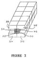
- Modules of the design shown in Figure 2 can be further combined in groups of four, as shown in Figure 3, to produce an even larger focal plane.
- four modules 302, 304, 306, and 308, each similar to the module illustrated in Figure 2 are combined to form a 10 element by 10 element focal plane made up of the four five by five element arrays 310, 312, 314, and 316 which are provided by the corresponding modules.
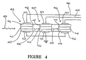
- Figure 4 is a cross-sectional side view of another edge illuminated detector array, which is similar to the array of Figure 1, except that in Figure 4 the array consists of solid state photomultiplier detectors.
- the first electrical contacts 422, 424, and 426, the second electrical contacts 428, 430, and 432, the optical axis of incoming optical energy 434, the portion 436 of optical energy transmitted by the first detector, the portion 438 of optical energy transmitted by the second detector, the line 440, the material 442, and the line 444 are all similar to the analogous elements described in connection with Figure 1.
- the series of three detectors 402, 404, and 406 each includes an extrinsic semiconducting active layer (layers 410, 412, and 414) with a first conductivity type impurity concentration which is high enough to create an impurity energy band.
- the second conductivity type impurity concentration in each active layer is low enough that first conductivity type carriers photogenerated in the active layer can drift through the active layer without recombining with ionized first conductivity type impurities.
- An intrinsic semiconducting blocking layer (layers 416, 418, and 420) in each detector is doped with first and second conductivity type impurity concentrations which are low enough that substantially no charge transport occurs by an impurity conduction mechanism.
- An extrinsic semiconducting buffered layer in each detector (layers 450, 452, and 454) has a first conductivity type impurity concentration which is high enough to create an impurity energy band and a second conductivity type impurity concentration which is high enough that first conductivity type carriers injected into the buffered layer will recombine with ionized first conductivity type impurities.
Landscapes
- Physics & Mathematics (AREA)
- Spectroscopy & Molecular Physics (AREA)
- General Physics & Mathematics (AREA)
- Engineering & Computer Science (AREA)
- Power Engineering (AREA)
- Electromagnetism (AREA)
- Condensed Matter Physics & Semiconductors (AREA)
- Computer Hardware Design (AREA)
- Microelectronics & Electronic Packaging (AREA)
- Light Receiving Elements (AREA)
- Photometry And Measurement Of Optical Pulse Characteristics (AREA)
Description
- This invention is concerned with the detection of electromagnetic radiation.
- The detection of electromagnetic energy is made possible because of a series of complex interactions which occur between such energy and certain kinds of materials. These interactions enable remote sensing systems to record contrasts between an observed object and its background. Recent improved detector designs based on the phenomenon of impurity band conduction (See U.S.-A-4,568,960 and U.S.-A-4,586,068) have significantly enhanced the power of the optical detectors available in the art. The output of these detectors in response to incident photons, however, depends on the total number of photons absorbed and does not provide information regarding the wavelengths of the photons which are absorbed.
- It would be desirable in some applications to be able to discriminate between optical sources having different spectral contents. A need has thus developed in the art for an impurity band conduction detector which can provide spectral discrimination.
- FR-A-2 285 720 discloses an edge illuminated optical detector array having plural detectors being arranged such that the impinging light successively passes through the detectors.
- The invention provides an optical focal plane according to claim 1 or 2. Subclaims 3 to 9 contain special features of the invention. The substrates and the arrays of this optical focal plane are positioned such that the first detectors in each series define a two dimensional focal plane.
- Additional details of the invention are described below in conjunction with the drawings, in which the same numerals are used to refer to like elements throughout all the figures. In the drawings:
- Figure 1 is a schematic cross sectional side view of an edge illuminated blocked impurity band detector array;
- Figure 2 is a perspective view of a detector focal plane which extends the detector array concept to two dimensional imaging;
- Figure 3 is a perspective view of a detector focal plane fabricated by combining four detector arrays similar to the array of Figure 2; and
- Figure 4 is a schematic cross sectional side view of an edge illuminated detector array similar to Figure 1, but using solid state photomultiplier detectors.
- It is an outstanding feature of this invention to provide an optical focal plane having a plurality of edge-illuminated detector arrays which exploit the optical transmission properties of extrinsic semiconductor materials to modify the spectral content of the optical energy which is applied to successive detectors in the array. Since the transmission properties of a doped semiconductor and the response characteristics of the detectors can be calibrated, and since the response of each detector in the array depends on the spectral content of the input to it, the spectral content of the radiation incident on the array can be derived from the relative response of each detector in the array. The detector arrays are intended to be made of impurity band conduction type detectors, such as blocked impurity band detectors and solid state photomultiplier detectors, the structure and operation of which are discussed in U.S.-A-4,568,960 (blocked impurity band detectors) and US-A-4,586,068 (solid state photomultiplier detectors). The teachings of these patents are incorporated by reference.
- Figure 1 is a schematic cross sectional side view of an edge illuminated blocked impurity band detector array. As those skilled in the art will appreciate, some of the spatial dimensions of the drawings are exaggerated relative to other dimensions in order to better explain the operation and features of the invention. Furthermore, an actual detector array may include additional components, such as a substrate, which are not included in the drawing since they do not play a role in the detection function which is the subject of this invention. A series of three
detectors layers layers contacts contacts optical energy 134, this direction being orthogonal to the direction of the applied bias. The incoming signal impinges on thefirst detector 102 in the series. A portion of the incoming energy is absorbed in and detected by the first detector, while theremainder 136 is transmitted by the first detector and impinges on thesecond detector 104. Similarly, theportion 138 of the optical energy which is transmitted by the second detector impinges on thethird detector 106. In this manner, the portion of the optical energy transmitted by each detector is directed to the succeeding detector in the series, so that the spectral content of the optical energy which impinges on each detector is modified by the spectral transmission characteristics of the preceding detectors. - Consider the detection mechanism for the first two
detectors first detector 102 and that detector will produce a commensurate electrical output signal on theline 140. The amount of photon absorption in the first detector and the output signal characteristics of the first detector will depend on the structural parameters of the first detector, such as impurity concentrations and detector dimensions. In any event, however, the first detector will selectively absorb the longer wavelength photons relatively more than the shorter wavelength photons, due to the properties of arsenic doped silicon. Thus, the spectral content of thephoton flux 136 exiting thefirst detector 102 and incident on thesecond detector 104 will be different than that of theincident energy 134. In particular, the spectral content of thesignal 136 will be relatively richer in shorter wavelength photons. Furthermore, if thematerial 142 which occupies the optical path between the first and second detectors is undoped silicon, this part of the path will be substantially transparent in the infrared spectral region. Part of the photons incident on thesecond detector 104 will be absorbed in that detector, which will generate a corresponding electrical output on theline 144. The second detector, like the first, will selectively absorb a greater fraction of the longer wavelength photons incident on it, so that thebeam 138 leaving the second detector will be relatively further depleted of long wavelength photons. - This mechanism may be effectively illustrated by considering a specific example. Assume that the first two detectors are identical in structure, there are no reflections at the interfaces, the absorption of λL in each detector is 40%, and the absorption of λS is 20%. Two different input signals, each having an equal number of total input photons, are postulated. The first input signal consists of 150 photons, 50 at λL and 100 at λS. When receiving the first signal, the first detector will produce an output proportional to 40 photons


- As this example shows, the relative responses of the two detectors will change with a change in the color or spectral content of the input to the detector array. The array of this invention thus provides the capability of extracting information about the color or spectral content of the incident beam. Note that for this capability to be effective, the input spectrum must be limited to the region where the relative absorption spectrum of the detector material is monotonic.
- While only two identical detectors have been treated in this example to simplify the analysis, those skilled in the art will appreciate that the invention contemplates the use of detectors of various sizes configured in a larger array to enable the resolution of several wavelengths. Furthermore, the simplifying assumptions which were made to illustrate the concept are not required constraints on this technique under more realistic conditions. Non-zero reflections at interfaces, for example, can be accounted for by analysis and calibration. In addition, the non-normal incidence of photons on the edge of the array can be tolerated to some extent, since the detector structure can be configured to guide the light waves within the active regions of the detectors. The optical transmission spectrum of each detector could also be tailored by selecting the dopant and host crystal materials used in fabrication.
- Figure 2 is a perspective view of a detector focal plane according to the invention, illustrating how the detector array concept can be extended to imaging a scene in two dimensions. The focal plane in this embodiment includes five
dice arrays arrays optical axis 232. Afocal plane 234 is created by aligning each array on all but the first die with a light pipe to convey optical energy from the focal plane to each detector array on the die. Thelight pipes die 210. The light pipes should preferably be fabricated of a transparent material with a coefficient of expansion similar to that of the detectors to avoid the problems which could otherwise arise when the focal plane array is cooled for operation at cryogenic temperatures. Several bonding pads, such as thepads - Modules of the design shown in Figure 2 can be further combined in groups of four, as shown in Figure 3, to produce an even larger focal plane. In Figure 3, four
modules element arrays - Figure 4 is a cross-sectional side view of another edge illuminated detector array, which is similar to the array of Figure 1, except that in Figure 4 the array consists of solid state photomultiplier detectors. The first
electrical contacts electrical contacts optical energy 434, theportion 436 of optical energy transmitted by the first detector, theportion 438 of optical energy transmitted by the second detector, theline 440, thematerial 442, and theline 444 are all similar to the analogous elements described in connection with Figure 1. In Figure 4, however, the series of threedetectors layers layers layers - The preferred embodiments of this invention have been illustrated and described above. Modifications and additional embodiments, however, will undoubtedly be apparent to those skilled in the art. The inventive concept, for example, is not limited either to the particular materials discussed herein nor to detection in the infrared region of the spectrum. Furthermore, equivalent elements may be substituted for those illustrated and described herein, parts or connections might be reversed or otherwise interchanged, and certain features of the invention may be utilized independently of other features. A number of alternative embodiments, for example, are described in the aforementioned patents and could be used for the detector arrays of this invention. Consequently, the exemplary embodiments should be considered illustrative, rather than inclusive, while the appended claims are indicative of the full scope of the invention.
Claims (9)
- An optical focal plane (234), comprising:
a plurality of substrates, each substrate including a row of a plurality of edge illuminated optical detector arrays (212, 214, ...), each array including a series of two or more detectors (102, 104, ...) for operation under an applied electrical field, each detector including:
an extrinsic semiconducting active layer (110, 112, ...) with a first conductivity type impurity concentration which is high enough to create an impurity energy band;
an intrinsic semiconducting blocking layer (116, 118, ...) with first and second conductivity type impurity concentrations which are low enough that substantially no charge transport occurs by an impurity conduction mechanism; and
first and second electrical contacts (122, 128, ...),
the active and blocking layers (110, 116, ...) being positioned between the contacts (122, 128, ...) such that an electrical potential applied to the contacts creates an electric field across the layers,
the detectors (102, 104, ...) within each array (212, 214, ...) being positioned relative to one another such that optical energy incident on the array and directed substantially orthogonal to the applied electric field impinges on the first detector in the series and such that the portion of the optical energy which is transmitted by each detector is directed to the succeeding detector in the series, so that the spectral content of the optical energy impinging on each detector is modified by the spectral transmission characteristics of the preceding detectors in the array, the rows of arrays in that substrates being positioned with an offset relationship such that the first detectors in each series define a two dimensional focal plane. - An optical focal plane (234), comprising:
a plurality of substrates, each substrate including a plurality of edge illuminated optical detector arrays (212, 214 ...), each array including a series of two or more detectors (402, 404, ...) for operation under an applied electric field, each detector including:
an extrinsic semiconducting buffered layer (450, 452, ...) with a first conductivity type impurity concentration which is high enough to create an impurity energy band and with a second conductivity type impurity concentration which is high enough that first conductivity type carriers injected into the buffered layer recombine with ionized first conductivity type impurities;
an intrinsic semiconducting blocking layer (416, 418, ...) with first and second conductivity type impurity concentrations which are low enough that substantially no charge transport occurs by an impurity conduction mechanism;
an extrinsic semiconducting active layer (410, 412, ...) between the blocking layer and the buffered layer with a first conductivity type impurity concentration which is high enough to create an impurity energy band and with a second conductivity type impurity concentration which is low enough that first conductivity type carriers photogenerated in the active layer can drift through the active layer without recombining with ionized first conductivity type impurities;
a first electrical contact (422, 424, ...) in contact with the blocking layer for collecting first conductivity type carriers without injecting second conductivity type carriers; and
a second electrical contact (428, 430, ...) in contact with the buffered layer for collecting carriers from the impurity band,
the buffered, active, and blocking layers being positioned between the contacts such that an electrical potential applied to the contacts creates an electric field across the layers,
the detectors (402, 404 ...) within each array being positioned relative to one another such that optical energy incident on the array and directed substantially orthogonal to the applied electric field impinges on the first detector in the series and such that the portion of the optical energy which is transmitted by each detector is directed to the succeeding detector in the series, so that the spectral content of the optical energy impinging on each detector is modified by the spectral transmission characteristics of the preceding detectors in the array, the rows of arrays in that substrates being positioned with an offset relationship such that the first detectors in each series define a two dimensional focal plane. - The optical focal plane of claims 1 and 2, wherein the first conductivity type impurities further comprise donor impurities and the second conductivity type impurities further comprise acceptor impurities.
- The optical focal plane of claims 1 and 2, wherein the first conductivity type impurities further comprise acceptor impurities and the second conductivity type impurities further comprise donor impurities.
- The optical focal plane of claims 1 and 2, wherein the blocking layer further comprises an undoped semiconducting layer.
- The optical focal plane of claim 1, wherein the blocking layer is epitaxially deposited on the active layer.
- The optical focal plane of claim 6, wherein the first contact further comprises a degenerately doped region or an ion implanted region in the blocking layer.
- The optical focal plane of claim 2, wherein the active layer is epitaxially deposited on the buffered layer and the blocking layer is epitaxially deposited on the active layer.
- The optical focal plane of claim 8, wherein the second contact further comprises a degenerately doped region or an ion implanted region in the buffered layer.
Applications Claiming Priority (2)
| Application Number | Priority Date | Filing Date | Title |
|---|---|---|---|
| US07/020,418 US4757210A (en) | 1987-03-02 | 1987-03-02 | Edge illuminated detector arrays for determination of spectral content |
| US20418 | 1987-03-02 |
Publications (3)
| Publication Number | Publication Date |
|---|---|
| EP0281011A2 EP0281011A2 (en) | 1988-09-07 |
| EP0281011A3 EP0281011A3 (en) | 1989-08-16 |
| EP0281011B1 true EP0281011B1 (en) | 1993-01-27 |
Family
ID=21798519
Family Applications (1)
| Application Number | Title | Priority Date | Filing Date |
|---|---|---|---|
| EP88102761A Expired - Lifetime EP0281011B1 (en) | 1987-03-02 | 1988-02-24 | Edge-illuminated impurity band conduction detector arrays |
Country Status (5)
| Country | Link |
|---|---|
| US (1) | US4757210A (en) |
| EP (1) | EP0281011B1 (en) |
| JP (1) | JPS63231230A (en) |
| CA (1) | CA1283968C (en) |
| DE (2) | DE3877785T4 (en) |
Families Citing this family (14)
| Publication number | Priority date | Publication date | Assignee | Title |
|---|---|---|---|---|
| DE68929444T2 (en) * | 1988-03-18 | 2003-10-02 | Nippon Sheet Glass Co., Ltd. | Self-scanning arrangement of light-emitting components |
| US4962304A (en) * | 1988-12-23 | 1990-10-09 | Rockwell International Corporation | Intrinsic impurity band conduction detectors |
| US5066994A (en) * | 1989-03-31 | 1991-11-19 | Eastman Kodak Company | Image sensor |
| US5001532A (en) * | 1989-09-06 | 1991-03-19 | Rockwell International Corporation | Impurity band conduction detector having photoluminescent layer |
| US4943491A (en) * | 1989-11-20 | 1990-07-24 | Honeywell Inc. | Structure for improving interconnect reliability of focal plane arrays |
| FR2713017B1 (en) * | 1993-11-23 | 1996-01-12 | Commissariat Energie Atomique | Radiation detector in two wavelength bands and method of manufacturing the detector. |
| WO2000010033A1 (en) * | 1995-10-05 | 2000-02-24 | Z.M.Z. Advanced Systems Ltd | Methods and apparatus for recording and reading-out an image formed by ionizing radiation |
| US7274011B2 (en) * | 2004-12-27 | 2007-09-25 | Teledyne Licensing, Llc | Spectral imager and fabrication method |
| WO2008104928A1 (en) * | 2007-03-01 | 2008-09-04 | Philips Intellectual Property & Standards Gmbh | Optical detector device |
| WO2013013246A1 (en) | 2011-07-21 | 2013-01-24 | Brooks Automation, Inc. | Method and device for compensation for dimensional variations in low temperature sample group holders |
| US11211305B2 (en) | 2016-04-01 | 2021-12-28 | Texas Instruments Incorporated | Apparatus and method to support thermal management of semiconductor-based components |
| US10861796B2 (en) | 2016-05-10 | 2020-12-08 | Texas Instruments Incorporated | Floating die package |
| US10074639B2 (en) | 2016-12-30 | 2018-09-11 | Texas Instruments Incorporated | Isolator integrated circuits with package structure cavity and fabrication methods |
| US10411150B2 (en) * | 2016-12-30 | 2019-09-10 | Texas Instruments Incorporated | Optical isolation systems and circuits and photon detectors with extended lateral P-N junctions |
Family Cites Families (6)
| Publication number | Priority date | Publication date | Assignee | Title |
|---|---|---|---|---|
| CA1003938A (en) * | 1974-09-17 | 1977-01-18 | Northern Electric Company, Limited | Photodiode detector with selective frequency response |
| US3987298A (en) * | 1975-07-09 | 1976-10-19 | Honeywell Inc. | Photodetector system for determination of the wavelength of incident radiation |
| US4568960A (en) * | 1980-10-23 | 1986-02-04 | Rockwell International Corporation | Blocked impurity band detectors |
| US4586068A (en) * | 1983-10-07 | 1986-04-29 | Rockwell International Corporation | Solid state photomultiplier |
| US4581625A (en) * | 1983-12-19 | 1986-04-08 | Atlantic Richfield Company | Vertically integrated solid state color imager |
| US4618763A (en) * | 1985-04-12 | 1986-10-21 | Grumman Aerospace Corporation | Infrared focal plane module with stacked IC module body |
-
1987
- 1987-03-02 US US07/020,418 patent/US4757210A/en not_active Expired - Fee Related
-
1988
- 1988-02-24 EP EP88102761A patent/EP0281011B1/en not_active Expired - Lifetime
- 1988-02-24 DE DE88102761T patent/DE3877785T4/en not_active Expired - Lifetime
- 1988-02-24 DE DE8888102761A patent/DE3877785D1/en not_active Expired - Fee Related
- 1988-02-25 JP JP63044052A patent/JPS63231230A/en active Pending
- 1988-02-26 CA CA000560000A patent/CA1283968C/en not_active Expired - Fee Related
Also Published As
| Publication number | Publication date |
|---|---|
| JPS63231230A (en) | 1988-09-27 |
| DE3877785T2 (en) | 1993-05-27 |
| US4757210A (en) | 1988-07-12 |
| EP0281011A3 (en) | 1989-08-16 |
| DE3877785T4 (en) | 1993-10-07 |
| CA1283968C (en) | 1991-05-07 |
| DE3877785D1 (en) | 1993-03-11 |
| EP0281011A2 (en) | 1988-09-07 |
Similar Documents
| Publication | Publication Date | Title |
|---|---|---|
| EP0281011B1 (en) | Edge-illuminated impurity band conduction detector arrays | |
| US5512750A (en) | A-dual band IR sensor having two monolithically integrated staring detector arrays for simultaneous, coincident image readout | |
| US5721429A (en) | Self-focusing detector pixel structure having improved sensitivity | |
| EP1280207B1 (en) | Semiconductor energy detector | |
| US4581625A (en) | Vertically integrated solid state color imager | |
| US4142198A (en) | Monolithic extrinsic silicon infrared detectors with an improved charge collection structure | |
| US5122669A (en) | Wideband schottky focal plane array | |
| US5751049A (en) | Two-color infrared detector | |
| GB1596978A (en) | Monolithic extrinsic silicon infrared detectors with charge-coupled readout | |
| US4586069A (en) | Opto-electrical device made of silicon for detecting infrared light | |
| EP0437102B1 (en) | Infrared image sensor and image pick-up apparatus using the same | |
| EP3794643A1 (en) | Short-wave infrared detector and its integration with cmos compatible substrates | |
| GB2208256A (en) | Infra-red radiation imaging devices and systems | |
| JPS6343366A (en) | Infrared detector | |
| US5517029A (en) | Dual-band IR scanning focal plane assembly having two monolithically integrated linear detector arrays for simultaneous image readout | |
| US4896202A (en) | Short wavelength impurity band conduction detectors | |
| EP0543537B1 (en) | Photodetector having reduced blind area | |
| US5438200A (en) | Composite photodetector substrate and method of forming the same | |
| US5066994A (en) | Image sensor | |
| WO1989005042A1 (en) | Reduced area photodiode junction | |
| Reine | Status of HgCdTe detector technology | |
| GB2239555A (en) | Infrared image-sensing devices and their manufacture | |
| GB2222722A (en) | Light detecting element and light detecting array | |
| US4727406A (en) | Pre-multiplexed detector array | |
| JPH05343729A (en) | Arrangement type infrared detector |
Legal Events
| Date | Code | Title | Description |
|---|---|---|---|
| PUAI | Public reference made under article 153(3) epc to a published international application that has entered the european phase |
Free format text: ORIGINAL CODE: 0009012 |
|
| AK | Designated contracting states |
Kind code of ref document: A2 Designated state(s): DE FR GB |
|
| PUAL | Search report despatched |
Free format text: ORIGINAL CODE: 0009013 |
|
| AK | Designated contracting states |
Kind code of ref document: A3 Designated state(s): DE FR GB |
|
| 17P | Request for examination filed |
Effective date: 19890925 |
|
| 17Q | First examination report despatched |
Effective date: 19901126 |
|
| GRAA | (expected) grant |
Free format text: ORIGINAL CODE: 0009210 |
|
| AK | Designated contracting states |
Kind code of ref document: B1 Designated state(s): DE FR GB |
|
| REF | Corresponds to: |
Ref document number: 3877785 Country of ref document: DE Date of ref document: 19930311 |
|
| ET | Fr: translation filed | ||
| PLBE | No opposition filed within time limit |
Free format text: ORIGINAL CODE: 0009261 |
|
| STAA | Information on the status of an ep patent application or granted ep patent |
Free format text: STATUS: NO OPPOSITION FILED WITHIN TIME LIMIT |
|
| 26N | No opposition filed | ||
| PGFP | Annual fee paid to national office [announced via postgrant information from national office to epo] |
Ref country code: FR Payment date: 19950113 Year of fee payment: 8 |
|
| PGFP | Annual fee paid to national office [announced via postgrant information from national office to epo] |
Ref country code: DE Payment date: 19950123 Year of fee payment: 8 |
|
| PGFP | Annual fee paid to national office [announced via postgrant information from national office to epo] |
Ref country code: GB Payment date: 19950126 Year of fee payment: 8 |
|
| PG25 | Lapsed in a contracting state [announced via postgrant information from national office to epo] |
Ref country code: GB Effective date: 19960224 |
|
| GBPC | Gb: european patent ceased through non-payment of renewal fee |
Effective date: 19960224 |
|
| PG25 | Lapsed in a contracting state [announced via postgrant information from national office to epo] |
Ref country code: FR Effective date: 19961031 |
|
| PG25 | Lapsed in a contracting state [announced via postgrant information from national office to epo] |
Ref country code: DE Effective date: 19961101 |
|
| REG | Reference to a national code |
Ref country code: FR Ref legal event code: ST |