EP0277638B1 - Successive period-to-voltage converting apparatus - Google Patents
Successive period-to-voltage converting apparatus Download PDFInfo
- Publication number
- EP0277638B1 EP0277638B1 EP88101480A EP88101480A EP0277638B1 EP 0277638 B1 EP0277638 B1 EP 0277638B1 EP 88101480 A EP88101480 A EP 88101480A EP 88101480 A EP88101480 A EP 88101480A EP 0277638 B1 EP0277638 B1 EP 0277638B1
- Authority
- EP
- European Patent Office
- Prior art keywords
- voltage
- signal
- pulse
- pulses
- clock
- Prior art date
- Legal status (The legal status is an assumption and is not a legal conclusion. Google has not performed a legal analysis and makes no representation as to the accuracy of the status listed.)
- Expired - Lifetime
Links
Images


Classifications
-
- G—PHYSICS
- G01—MEASURING; TESTING
- G01R—MEASURING ELECTRIC VARIABLES; MEASURING MAGNETIC VARIABLES
- G01R23/00—Arrangements for measuring frequencies; Arrangements for analysing frequency spectra
- G01R23/02—Arrangements for measuring frequency, e.g. pulse repetition rate; Arrangements for measuring period of current or voltage
- G01R23/06—Arrangements for measuring frequency, e.g. pulse repetition rate; Arrangements for measuring period of current or voltage by converting frequency into an amplitude of current or voltage
-
- G—PHYSICS
- G04—HOROLOGY
- G04F—TIME-INTERVAL MEASURING
- G04F10/00—Apparatus for measuring unknown time intervals by electric means
- G04F10/10—Apparatus for measuring unknown time intervals by electric means by measuring electric or magnetic quantities changing in proportion to time
- G04F10/105—Apparatus for measuring unknown time intervals by electric means by measuring electric or magnetic quantities changing in proportion to time with conversion of the time-intervals
Definitions
- the present invention relates to a successive period-to-voltage converting apparatus which is suitable for use in the measurement of a variance in the speed of, for instance, a motor or engine.
- the duration of an input pulse i.e. its time length is usually measured by use of such an apparatus as disclosed in US-A-4,611,926, for example.
- This apparatus includes a gate circuit, a clock generator, and a counter. With this apparatus, the gate circuit is kept open during the duration of the input pulse, the number of clock pulses from the clock generator, which have passed through the gate circuit, is counted by the counter, and then the count value is obtained as a value corresponding to the measured pulse width.
- the measurement accuracy of such an apparatus is dependent on the frequency of clock pulses used; for example, when a 10 MHz clock is used, resolution of the measured time length will be 100 nsec.
- the frequency at which the counter is operable is 500 MHz at the highest, and when a 500 MHz clock is utilized, the accuracy of time measurement will be 2 nsec or so. Accordingly, it is difficult, with such a time measuring apparatus, to conduct the time measurement with a higher degree of accuracy.
- the above-mentioned apparatus is so arranged as to successively measure the widths of a series of pulses.
- this apparatus is applied to the measurement of pulse periods, for instance, only alternate pulse periods such as those from first to second pulse, from third to fourth pulse, from fifth to sixth pulse, etc. are usually measured, but the periods from the second to third pulse, from the fourth to fifth pulse, etc. are not measured.
- This defect will constitute a serious obstacle to the measurement of a variance in the speed of a precision motor or accurate measurement of a variance in the speed of an engine.
- a pulse generator is provided in association with the rotary shaft to be measured, at least one pulse is generated by the pulse generator for each rotation of the rotary shaft, and the time intervals each between two successive such pulses are measured, thereby measuring the variance in the rotating speed.
- An apparatus according to the precharacterizing clause of claim 1 is disclosed in EP-A-0 165 144.
- the apparatus of this document is only capable to measure time intervals between first and second signals, between third and fourth signals, between fifth and sixth signals and so on, but is not capable of measuring those between the second and third signals, between fourth and fifth signals and so on.
- US-A-4 112 358 discloses a digital frequency measuring device including converting means, which are fed with signals in a simultaneous manner while their outputs are supplied simultaneously to an A-D-converter. Moreover, this document does not mention to reset one of said converting means after stopping the integration by the other one.
- the object underlying the invention is to provide a successive period-to-voltage converting apparatus which is capable of measuring the intervals between all the appearing signals to thus improve period or frequency measurement, respectively.
- a fractional time between each of successive input pulses and a corresponding clock pulse is converted into a voltage signal, by alternate one of first and second fractional time-to-voltage converters.
- the voltage signals from the two converters are applied to a change-over switch, in which the distribution of the voltage signals is switched so that an earlier one of the two successive voltage signals is always provided on one fixed signal path, the later voltage signal on the other fixed signal path.
- the two voltage signals thus switched are provided to an analog subtractor, wherein the later fractional time is always subtracted from the earlier one, obtaining a difference signal therebetween. Accordingly, this difference signal can be obtained for each period of the input pulse.
- the number of clock pulses which are present in the period between two successive input pulses is counted by a counter, and the count value is converted by a D-A converter into an analog voltage corresponding to the number of clock pulses counted.
- the analog voltage and the difference signal are applied to an adder, wherein they are added together, thereby obtaining the time interval between the successive two input pulses.
- the present invention permits measurement of the period defined by successive two input pulses, for example. Accordingly, the present invention, when applied to the measurement of a variance in the speed of a rotating machine, allows continuous measurement of the state of rotation of its rotary shaft.
- T Letting a reference clock period be represented by To, the time interval T to be measured is given by the following expression: where N is the number of clock pulses which are counted for the duration of an input signal S, T n is the time interval from a clock pulse generated immediately after the rise of the input signal S to a clock pulse generated immediately after the fall of the input signal S, that is, N'To, and ⁇ t 1 and ⁇ t 2 are fractional times from the rise and fall of the input signal S to the clock pulses appearing directly after them, respectively.
- the counting of clock pulses for measuring the time interval T n need not always be conducted within the time interval T to be measured alone, but the counting may also be effected from the clock pulse appearing immediately after the initiation of the interval T n to the clock pulse at the end thereof.
- the purpose could also be served by similarly counting the clock pulses for a period delayed behind the interval T n by a predetermined number of clocks.
- the time interval T is obtained with high accuracy, based on expression (1), by counting the number of clock pulses N through use of a counter and accurately measuring the fractional times OT, and ⁇ T 2 by some method.
- Fig. 2 illustrates an embodiment of the present invention.
- the basic arrangement of the period-to-voltage converting apparatus of the present invention includes: a signal detector 102 which detects the leading or trailing edge (hereinafter only the leading edge will be referred to, for the sake of brevity) of each input pulse which is applied to an input terminal 101; first and second fractional time-to-voltage converters 103 and 104 which alternatively convert to a voltage signal, for a series of input pulse, a fractional time which is defined by starting an integration with the detected output from the signal detector 102 and stopping the integration upon arrival of a predetermined number (K) of clock pulses after the initiation of the integration, that is, defined by the time interval between the rise of each input pulse and the termination of the integration; a change-over switch 105 by which earlier and later ones of two successive voltage signals from the first and second fractional time-to-voltage converters 103 and 104, in terms of the order of the time series of the corresponding input pulses, are provided on fixed
- a reset signal shown in Fig. 3A is generated, which is applied to respective parts of the apparatus, resetting them to their initial states.
- the signal detector 102 in this embodiment is formed by a JK flip-flop.
- the JK flip-flop 102 is supplied at its trigger terminal T with a series of input pulses (see Fig. 3B) applied to the input terminal 101.
- the JK flip-flop 102 provides, at its output terminals Q and Q, opposite-polarity rectangular waves @ and shown in Fig. 3D and 3E.
- the rectangular waves @ and are applied to the first and second fractional time-to-voltage converters 103 and 104, respectively.
- the first and second fractional time-to-voltage (hereinafter simplified at T-V) converters 103 and 104 can each be constituted as shown in Fig. 4 by a D flip-flop 302, a level converter 303, an analog integration circuit 306, an analog switch 307 for controlling the supply of an integration voltage to the analog integration circuit 306, and an integration time control circuit 308.
- reference numeral 301 indicates an input terminal of each of the first and second fractional T-V converters 103 and 104.
- the D flip-flop 302 Before the application of the rectangular wave @ or to the input terminal 301 the D flip-flop 302 remains in its reset state and an L logic of its Q output holds the integration time control circuit 308 in its reset state.
- the rectangular wave @ or is supplied from the signal detector 102 via the input terminal 301 to the trigger terminal T of the D flip-flop 302.
- the D flip-flop 302 is always supplied at its data input terminal D with an H-logic signal.
- the D flip-flop 302 reads thereinto the H logic at the timing of the rise of the rectangular wave @ or and provides the H logic at its output terminal Q.
- the output of the D flip-flop 302 is supplied to the analog integration circuit 306 via a buffer 304 which forms the level converter 303.
- the analog integration circuit 306 is made up of an operational amplifier 311, an integrating capacitor 312 connected between input and output terminals of the operational amplifier 311, a switch 313 connected in parallel to the integrating capacitor 312, and an integrating resistor 314.
- the switch 313 of the analog integration circuit 306 is normally held in the ON state, discharging charges stored in the integrating capacitor 312.
- the switch 313 is turned OFF.
- the integration time control circuit 308 is released from its reset state.
- a flip-flop 316 which forms the integration time control circuit 308, is released from its initialized reset state and until it is supplied at its trigger terminal T with a trigger signal, it provides an L-logic output at its Q output, retaining the analog switch 307 in the ON state. Accordingly, when the switch 313 is turned ON by the Q output from the afore-said flip-flop 302, the analog integration circuit 306 immediately starts an integration.
- the integration time of the analog integration circuit 306 is defined by the frequency dividing ratio 1/K of a frequency divider 315 which forms the integration time control circuit 308. That is, when released from its reset state by the Q output of the flip-flop 302, the frequency divided 315 frequency divides the clock pulses @ and, when having counted K clock pulses, it applies the trigger signal to the flip-flop 316.
- the flip-flop 316 When supplied with the trigger signal, the flip-flop 316 reads thereinto an H-logic input applied at its data terminal and provides an H-logic output at its output terminal Q, turning OFF the analog switch 307.
- the integration time of each of the first and second fractional T-V converters 103 and 104 is thus defined to the time from the rise of the input pulse 02 to the application of the K-th clock pulse @.
- the integrating operation stops when the supply of an integrating voltage -E to the analog integration circuit 306 is stopped upon turning-OFF of the analog switch 307.
- One of the fractional T-V converters is kept out of the integrating operation until after the next input pulse is applied and its fractional time is converted by the other fractional T-V converter into a voltage signal, as shown in Fig. 3S or 3T.
- the fractional time of the next input pulse is converted by the other fractional T-V converter into the voltage signal in the same manner as described above.
- the voltage signals corresponding to the two fractional times, thus obtained with the two fractional T-V converters 103 and 104, are provided to the analog subtractor 106, wherein a later one of the voltage signal is subtracted from the earlier voltage signal, obtaining the difference therebetween as depicted in Fig. 3U.
- a reset signal @ or @ is applied via an OR gate 318 to a reset terminal R of the D flip-flop 302, resetting the fractional T-V converters 103 and 104.
- An AND gate 317 constitutes means for extracting a signal representing the state in which the fractional time is being converted into the voltage signal, and the AND gate 317 provides at an output terminal 319 a pulse or shown in Fig. 3F or 3G.
- the pulse or is applied to a controller 115, wherein it is utilized for the generation of control signals which are used in respective parts.
- the controller 115 comprises OR gates 116, 117, 118 and 119, AND gates 121, 122, 123 and 124, JK flip-flops 125, 126 and 127, a D flip-flop 128, a frequency divider 129, and monostable multivibrators 131 and 132.
- the OR gate 116 forms means by which the pulses and from the fractional T-V converters 103 and 104 are combined into a signal of one series.
- the pulse thus obtained is applied to a trigger terminal T of the JK flip-flop 125 via the OR gate 117 and a trigger terminal T of the JK flip-flop 126 via the AND gate 123 and the OR gate 118.
- the JK flip-flop 126 yields a rectangular wave signal @ depicted in Fig. 3K.
- the rectangular wave signal @ is applied to the AND gate 107, through which the clock pulses from a clock generator 110 are provided to the counter 108 while the rectangular wave signal @ is high-level.
- Fig. 3L shows the pulses @ which are applied to the counter 108.
- the counter 108 counts the pulses @ and the count value is converted by the D-A converter 109 to an analog voltage @ , which is provided to the adder 111.
- a processing time ⁇ M is provided for producing an output voltage corresponding to a period in connection with each input pulse and discharging the integrating capacitors 312 in the first and second fractional T-V converters 103 and 104 by pulses and @ .
- the processing time ⁇ M begins at a clock pulse where the integrating operation of each of the fractional T-V converters 103 and 104 completes and ends at the time point of having counted M clock pulses.
- the count value of the counter 108 is set to a value smaller than the actual one by M.
- this embodiment employs a presetable counter as the counter 108, and in the initial state in which it starts the counting, a numerical value M preset in a register 120 is preset in the counter 108 so that the latter may start the counting from the preset value M.
- a control signal @ for controlling the change-over switch 105 is produced by the JK flip-flop 127.
- the JK flip-flop 127 yields the control signal 13 of a rectangular wave which reverses its polarity upon each fall of a signal , i.e. upon each termination of the processing time TM , as depicted in Fig. 3M.
- the control signal @ is applied to the change-over switch 105 to control its switching operation.
- the change-over switch 105 is arranged so that its movable contacts C are connected to contacts A or B, depending on whether the control signal @ is high- or low-level.
- the change-over switch 105 provides therethrough the output of the first fractional T-V converter 103 onto the signal path 113 and the output of the second fractional T-V converter 104 onto the signal path 114.
- the change-over switch 105 provides therethrough the output of the first fractional T-V converter 103 onto the signal path 114 and the output of the second fractional T-V converter 104 onto the signal path 113.
- Fig. 5 illustrates a specific operative example of the change-over switch 105.
- the control signal @ is applied to a control input terminal 401, from which it is provided via a level converter 402 to gates of switching elements 403 to 406, turning ON and OFF the switching elements 403 and 406 and those 404 and 405 alternately with each other each time a fixed time interval M x To has elapsed after completion of the integration at either of the first and second fractional T-V converters 103 and 104.
- a fraction signal ⁇ v 2m-1 from the first fractional T-V converter 103 and a fraction signal ⁇ v 2m from the second fractional T-V converter 104 are alternately switched between them, and a fraction signal Av n obtained with respect to one input pulse is provided on the signal path 113 and a fraction signal ⁇ v n+1 obtained with respect to the next input pulse is provided on the signal path 114.
- the signal paths 113 and 114 are connected to plus and minus terminals of the analog subtractor 106, respectively.
- the subtraction of the output of the second fractional T-V converter 104 from the output of the first fractional T-V converter 103 and the subtraction of the latter from the former can alternately be switched between them, by controlling the change-over switch 105 to switch in synchronism with the period of the input pulse .
- the analog subtractor 106 yields at its output a difference signal by subtracting, from the voltage signal AV n obtained at the preceding timing, the voltage signal ⁇ V n+1 obtained at the current timing, that is, AV n - ⁇ V n+1 (Fig. 3U).
- the difference signal @ from the analog subtractor 106 and the output signal @ (Fig. 3V) from the D-A converter 109 are added together by the adder 111.
- the added output from the adder 111 is sample-held in a sample hold circuit 112, the output of which is provided at an output terminal 133.
- the sample holding by the sample hold circuit 112 is timed by a pulse (Fig. 30) which is yielded from the monostable multivibrator 131.
- the pulse from the monostable multivibrator 131 is also applied to the monostable multivibrator 132. At the timing of the fall of the pulse the monostable multivibrator 132 is triggered, generating the pulse .
- the pulse @ is provided via the OR gate 119 to a preset terminal PS of the counter 108, presetting therein the initial value M at the rise of the pulse , for instance.
- the pulse @ is applied to the two AND gates 121 and 122 as well. These two AND gates 121 and 122 are controlled to be enabled and disabled alternately with each other, by the control signal @ from the JK flip-flop 127, in synchronism with the period of the input pulse . Accordingly, the successive pulses @ are distributed, by the two AND gates 121 and 122, into pulse signals and of two series, as shown in Figs. 3Q and 3R. The pulse signals and of the two series are provided to the first and second fractional T-V converters 103 and 104, respectively, thereby alternately initializing their integration circuits 306 and integration time control circuits 308.
- periods Pi, P 2 , ... are expressed, from the timing chart of Fig. 3, in the same manner as expression (1), as follows:
- ⁇ T n and ⁇ T n+1 are elapsed times from the rise of nth and (n + 1)th input pulses to Kth clock pulses, respectively, K being determined by the frequency dividing number of the frequency divider 315 included in the integration time control circuit 308 and being selected equal to or greater than 2.
- the value of N n indicates the count value of the counter 108 shown in Fig. 1.
- the counter 108 is a presetable counter, in which the frequency dividing number M of the frequency divider 129 is preset.
- the frequency dividing number M of the frequency divider 129 is chosen so that it may bear the following relationship to ⁇ S and ⁇ P shown in Fig. 3.
- To is the clock period
- ⁇ S is a sample time for the sample hold circuit 112
- ⁇ P is the time for presetting the counter 108 or resetting each of the fractional T-V converters 103 and 104.
- the counted output N n of the counter 108 is applied to the D-A converter 109, by which it is converted into a voltage N n ⁇ V 0 , where Vo is a constant step of voltage value by which the output voltage signal @ of the D-A converter 109 varies whenever the counter 108 is incremented of decremented by one.
- the voltage value Vo is selected 10 times larger than the minimum resolution of the D-A converter 109 when a digit one order lower than the digit of Vo is assigned to the value of the difference signal .
- Fig. 6 illustrates a specific operative example of the analog subtractor 106.
- the amplification factor R 2 /Ri that is needed for the analog subtractor 106 is as follows:
- each period P n of successive two input pulses given by expression (1) can be converted, by use of expressions (8), (9), (10) and (14), into the voltage V n given by the following expression:
- Fig. 7 illustrates a specific operative example of the adder 111. Letting values of resistors 601 and 602 be equal to each other and be represented by R 3 and the value of a resistor 603 by R 4 , the amplification factor of the adder 111 is determined by R 4 /R 3 .
- Vn of the input signal (AV n - ⁇ V n+1 ) and the D-A converter output N n ⁇ V 0 is provided in the following form: Comparison of expressions (15) and (16) shows that the output voltage Vn of the adder 111 is proportional to the voltage V n and hence proportional to the period P n .
- the gate signal shown in Fig. 3K is substantially the same as an inverted version of the signal shown in Fig. 31, and accordingly the Q output of the flip-flop 125 may also be applied, as a gate signal, directly to the AND gate 107.
- the AND gate 123, and OR gate 118, and the flip-flop 126 can be dispensed with.
- 3W may be simply ignored, it is also possible to utilize an arrangement in which the flip-flop 128 and the AND gate 124 are further omitted and the Q output of the flip-flop 125 is applied directly to the trigger terminal T of the monostable multivibrator 131.
- the fractional times between the successive input pulses and the clock pulses @ are measured by the pair of fractional T-V converters 103 and 104 alternately with each other, and the measured outputs are applied to the change-over switch 105, the switching operation of which allows the subtractor 106 to subtract, from the fractional time obtained in relation to any input pulse, the fractional time obtained in relation to the next input pulse.
- a voltage waveform corresponding to a variance in the speed of a rotating member can be displayed on the oscilloscope.
- a frequency analysis can be made of a variance in the speed of the rotating member. Accordingly, a variance in the speed of a rotating machine such as a precision motor or engine can be measured with high precision.
Landscapes
- Physics & Mathematics (AREA)
- General Physics & Mathematics (AREA)
- Analogue/Digital Conversion (AREA)
- Measurement Of Unknown Time Intervals (AREA)
- Measuring Frequencies, Analyzing Spectra (AREA)
- Control Of Electric Motors In General (AREA)
Description
- The present invention relates to a successive period-to-voltage converting apparatus which is suitable for use in the measurement of a variance in the speed of, for instance, a motor or engine.
- The duration of an input pulse, i.e. its time length is usually measured by use of such an apparatus as disclosed in US-A-4,611,926, for example. This apparatus includes a gate circuit, a clock generator, and a counter. With this apparatus, the gate circuit is kept open during the duration of the input pulse, the number of clock pulses from the clock generator, which have passed through the gate circuit, is counted by the counter, and then the count value is obtained as a value corresponding to the measured pulse width. The measurement accuracy of such an apparatus is dependent on the frequency of clock pulses used; for example, when a 10 MHz clock is used, resolution of the measured time length will be 100 nsec. At present, however, the frequency at which the counter is operable is 500 MHz at the highest, and when a 500 MHz clock is utilized, the accuracy of time measurement will be 2 nsec or so. Accordingly, it is difficult, with such a time measuring apparatus, to conduct the time measurement with a higher degree of accuracy.
- Furthermore, the above-mentioned apparatus is so arranged as to successively measure the widths of a series of pulses. When this apparatus is applied to the measurement of pulse periods, for instance, only alternate pulse periods such as those from first to second pulse, from third to fourth pulse, from fifth to sixth pulse, etc. are usually measured, but the periods from the second to third pulse, from the fourth to fifth pulse, etc. are not measured.
- This defect will constitute a serious obstacle to the measurement of a variance in the speed of a precision motor or accurate measurement of a variance in the speed of an engine.
- For measuring a variance in the speed of a rotating machine, it is customary in the art to employ a method in which a pulse generator is provided in association with the rotary shaft to be measured, at least one pulse is generated by the pulse generator for each rotation of the rotary shaft, and the time intervals each between two successive such pulses are measured, thereby measuring the variance in the rotating speed.
- With the afore-mentioned apparatus which can measure the time interval every other pulse alone, a variance in the speed of the rotary shaft is measured only every other rotation thereof. Accordingly, the state of rotation of the rotary shaft cannot continuously be measured.
- Even if a plurality of pulses are produced for each rotation of the rotary shaft, it is still impossible to measure the state of a continuous variance in the speed of the rotary shaft during one rotation thereof.
- An apparatus according to the precharacterizing clause of
claim 1 is disclosed in EP-A-0 165 144. The apparatus of this document is only capable to measure time intervals between first and second signals, between third and fourth signals, between fifth and sixth signals and so on, but is not capable of measuring those between the second and third signals, between fourth and fifth signals and so on. - US-A-4 112 358 discloses a digital frequency measuring device including converting means, which are fed with signals in a simultaneous manner while their outputs are supplied simultaneously to an A-D-converter. Moreover, this document does not mention to reset one of said converting means after stopping the integration by the other one.
- Therefore, the object underlying the invention is to provide a successive period-to-voltage converting apparatus which is capable of measuring the intervals between all the appearing signals to thus improve period or frequency measurement, respectively.
- According to the invention the above object is achieved by an apparatus as claimed.
- According to the present invention, a fractional time between each of successive input pulses and a corresponding clock pulse is converted into a voltage signal, by alternate one of first and second fractional time-to-voltage converters. The voltage signals from the two converters are applied to a change-over switch, in which the distribution of the voltage signals is switched so that an earlier one of the two successive voltage signals is always provided on one fixed signal path, the later voltage signal on the other fixed signal path. The two voltage signals thus switched are provided to an analog subtractor, wherein the later fractional time is always subtracted from the earlier one, obtaining a difference signal therebetween. Accordingly, this difference signal can be obtained for each period of the input pulse.
- On the other hand, the number of clock pulses which are present in the period between two successive input pulses is counted by a counter, and the count value is converted by a D-A converter into an analog voltage corresponding to the number of clock pulses counted.
- The analog voltage and the difference signal are applied to an adder, wherein they are added together, thereby obtaining the time interval between the successive two input pulses.
- As described above, the present invention permits measurement of the period defined by successive two input pulses, for example. Accordingly, the present invention, when applied to the measurement of a variance in the speed of a rotating machine, allows continuous measurement of the state of rotation of its rotary shaft.
-
- Fig. 1 is a timing chart, for explaining the known principle of time interval measurement;
- Fig. 2 is a block diagram illustrating an embodiment of the present invention;
- Figs. 3A through 3W are waveform diagrams, for explaining the operation of the present invention;
- Fig. 4 is a circuit diagram showing a specific operative example of a fractional time-to-voltage converter for use in the embodiment of the present invention;
- Fig. 5 is a circuit diagram showing a specific operative example of a change-over switch for use in the embodiment of the present invention;
- Fig. 6 is a circuit diagram showing a specific operative example of an analog subtractor for use in the present invention; and
- Fig. 7 is a circuit diagram showing a specific operative example of an adder for use in the embodiment of the present invention.
- A description will be given first, with reference to Fig. 1, of the known principle of measuring a time interval T. Letting a reference clock period be represented by To, the time interval T to be measured is given by the following expression:


- Fig. 2 illustrates an embodiment of the present invention. The basic arrangement of the period-to-voltage converting apparatus of the present invention includes: a
signal detector 102 which detects the leading or trailing edge (hereinafter only the leading edge will be referred to, for the sake of brevity) of each input pulse which is applied to aninput terminal 101; first and second fractional time-to-voltage converters signal detector 102 and stopping the integration upon arrival of a predetermined number (K) of clock pulses after the initiation of the integration, that is, defined by the time interval between the rise of each input pulse and the termination of the integration; a change-overswitch 105 by which earlier and later ones of two successive voltage signals from the first and second fractional time-to-voltage converters fixed signal paths analog subtractor 106 which obtains a difference signal between the voltage signals provided from the change-overswitch 105, by subtracting the later voltage signal from the earlier one; agate 107 for extracting clock pulses present in an interval corresponding to each period defined by the successive two input pulses; acounter 108 for counting the clock pulses extracted by thegate 107; aD-A converter 109 for converting the count value of thecounter 108 to analog form; and anadder 111 for adding together the voltage signal from theD-A converter 109 and the difference signal from theanalog subtractor 106. - When the power supply of the period-to-voltage converting apparatus is turned ON, a reset signal shown in Fig. 3A is generated, which is applied to respective parts of the apparatus, resetting them to their initial states. The
signal detector 102 in this embodiment is formed by a JK flip-flop. The JK flip-flop 102 is supplied at its trigger terminal T with a series of input pulses (see Fig. 3B) applied to theinput terminal 101. - The JK flip-
flop 102 provides, at its output terminals Q and Q, opposite-polarity rectangular waves @ and shown in Fig. 3D and 3E. The rectangular waves @ and are applied to the first and second fractional time-to-voltage converters - The first and second fractional time-to-voltage (hereinafter simplified at T-V)
converters flop 302, alevel converter 303, ananalog integration circuit 306, ananalog switch 307 for controlling the supply of an integration voltage to theanalog integration circuit 306, and an integrationtime control circuit 308. - In Fig. 4
reference numeral 301 indicates an input terminal of each of the first and secondfractional T-V converters input terminal 301 the D flip-flop 302 remains in its reset state and an L logic of its Q output holds the integrationtime control circuit 308 in its reset state. The rectangular wave @ or is supplied from thesignal detector 102 via theinput terminal 301 to the trigger terminal T of the D flip-flop 302. The D flip-flop 302 is always supplied at its data input terminal D with an H-logic signal. - With the above arrangement, the D flip-
flop 302 reads thereinto the H logic at the timing of the rise of the rectangular wave @ or and provides the H logic at its output terminal Q. The output of the D flip-flop 302 is supplied to theanalog integration circuit 306 via abuffer 304 which forms thelevel converter 303. - The
analog integration circuit 306 is made up of anoperational amplifier 311, anintegrating capacitor 312 connected between input and output terminals of theoperational amplifier 311, a switch 313 connected in parallel to theintegrating capacitor 312, and anintegrating resistor 314. - The switch 313 of the
analog integration circuit 306 is normally held in the ON state, discharging charges stored in the integratingcapacitor 312. When the rectangular wave @ or , which is applied to theinput terminal 301 of the one fractional T-V converter, rises and the D flip-flop 302 yields the H-logic output, the switch 313 is turned OFF. At the same time, the integrationtime control circuit 308 is released from its reset state. A flip-flop 316, which forms the integrationtime control circuit 308, is released from its initialized reset state and until it is supplied at its trigger terminal T with a trigger signal, it provides an L-logic output at its Q output, retaining theanalog switch 307 in the ON state. Accordingly, when the switch 313 is turned ON by the Q output from the afore-said flip-flop 302, theanalog integration circuit 306 immediately starts an integration. - The integration time of the
analog integration circuit 306 is defined by thefrequency dividing ratio 1/K of afrequency divider 315 which forms the integrationtime control circuit 308. That is, when released from its reset state by the Q output of the flip-flop 302, the frequency divided 315 frequency divides the clock pulses @ and, when having counted K clock pulses, it applies the trigger signal to the flip-flop 316. - When supplied with the trigger signal, the flip-
flop 316 reads thereinto an H-logic input applied at its data terminal and provides an H-logic output at its output terminal Q, turning OFF theanalog switch 307. In this embodiment the integration time of each of the first and second fractionalT-V converters - The integrating operation stops when the supply of an integrating voltage -E to the
analog integration circuit 306 is stopped upon turning-OFF of theanalog switch 307. One of the fractional T-V converters is kept out of the integrating operation until after the next input pulse is applied and its fractional time is converted by the other fractional T-V converter into a voltage signal, as shown in Fig. 3S or 3T. - The fractional time of the next input pulse is converted by the other fractional T-V converter into the voltage signal in the same manner as described above. The voltage signals corresponding to the two fractional times, thus obtained with the two fractional
T-V converters analog subtractor 106, wherein a later one of the voltage signal is subtracted from the earlier voltage signal, obtaining the difference therebetween as depicted in Fig. 3U. When the difference is thus obtained, a reset signal @ or @ is applied via anOR gate 318 to a reset terminal R of the D flip-flop 302, resetting the fractionalT-V converters - An AND
gate 317 constitutes means for extracting a signal representing the state in which the fractional time is being converted into the voltage signal, and the ANDgate 317 provides at an output terminal 319 a pulse or shown in Fig. 3F or 3G. The pulse or is applied to acontroller 115, wherein it is utilized for the generation of control signals which are used in respective parts. - Turning back to Fig. 2, the
controller 115 comprises ORgates gates flops flop 128, afrequency divider 129, andmonostable multivibrators - The OR
gate 116 forms means by which the pulses and from the fractionalT-V converters flop 125 via the OR gate 117 and a trigger terminal T of the JK flip-flop 126 via the ANDgate 123 and theOR gate 118. - The JK flip-
flop 126 yields a rectangular wave signal @ depicted in Fig. 3K. The rectangular wave signal @ is applied to the ANDgate 107, through which the clock pulses from aclock generator 110 are provided to thecounter 108 while the rectangular wave signal @ is high-level. Fig. 3L shows the pulses @ which are applied to thecounter 108. Thecounter 108 counts the pulses @ and the count value is converted by theD-A converter 109 to an analog voltage @ , which is provided to theadder 111. - A processing time τM is provided for producing an output voltage corresponding to a period in connection with each input pulse and discharging the integrating
capacitors 312 in the first and second fractionalT-V converters T-V converters - To provide the processing time TM, the count value of the
counter 108 is set to a value smaller than the actual one by M. On this account, this embodiment employs a presetable counter as thecounter 108, and in the initial state in which it starts the counting, a numerical value M preset in aregister 120 is preset in thecounter 108 so that the latter may start the counting from the preset value M. - A control signal @ for controlling the change-
over switch 105 is produced by the JK flip-flop 127. The JK flip-flop 127 yields thecontrol signal 13 of a rectangular wave which reverses its polarity upon each fall of a signal , i.e. upon each termination of the processing time TM, as depicted in Fig. 3M. The control signal @ is applied to the change-over switch 105 to control its switching operation. In this embodiment, the change-over switch 105 is arranged so that its movable contacts C are connected to contacts A or B, depending on whether the control signal @ is high- or low-level. - With the movable contacts C connected to the contacts A, the change-
over switch 105 provides therethrough the output of the firstfractional T-V converter 103 onto thesignal path 113 and the output of the secondfractional T-V converter 104 onto thesignal path 114. With the movable contacts C connected to the contacts B, the change-over switch 105 provides therethrough the output of the firstfractional T-V converter 103 onto thesignal path 114 and the output of the secondfractional T-V converter 104 onto thesignal path 113. - Fig. 5 illustrates a specific operative example of the change-
over switch 105. The control signal @ is applied to acontrol input terminal 401, from which it is provided via alevel converter 402 to gates of switchingelements 403 to 406, turning ON and OFF the switchingelements T-V converters fractional T-V converter 103 and a fraction signal Δv2m from the secondfractional T-V converter 104 are alternately switched between them, and a fraction signal Avn obtained with respect to one input pulse is provided on thesignal path 113 and a fraction signal △vn+1 obtained with respect to the next input pulse is provided on thesignal path 114. Thesignal paths analog subtractor 106, respectively. - With such an arrangement, the subtraction of the output of the second
fractional T-V converter 104 from the output of the firstfractional T-V converter 103 and the subtraction of the latter from the former can alternately be switched between them, by controlling the change-over switch 105 to switch in synchronism with the period of the input pulse . - As a result of this, the
analog subtractor 106 yields at its output a difference signal by subtracting, from the voltage signal AVn obtained at the preceding timing, the voltage signal △Vn+1 obtained at the current timing, that is, AVn - △Vn+1 (Fig. 3U). The difference signal @ from theanalog subtractor 106 and the output signal @ (Fig. 3V) from theD-A converter 109 are added together by theadder 111. The added output from theadder 111 is sample-held in asample hold circuit 112, the output of which is provided at anoutput terminal 133. The sample holding by thesample hold circuit 112 is timed by a pulse (Fig. 30) which is yielded from themonostable multivibrator 131. The pulse from themonostable multivibrator 131 is also applied to themonostable multivibrator 132. At the timing of the fall of the pulse themonostable multivibrator 132 is triggered, generating the pulse . The pulse @ is provided via theOR gate 119 to a preset terminal PS of thecounter 108, presetting therein the initial value M at the rise of the pulse , for instance. - The pulse @ is applied to the two AND
gates gates flop 127, in synchronism with the period of the input pulse . Accordingly, the successive pulses @ are distributed, by the two ANDgates T-V converters integration circuits 306 and integrationtime control circuits 308. - In the embodiment described above, periods Pi, P2, ... are expressed, from the timing chart of Fig. 3, in the same manner as expression (1), as follows:



frequency divider 315 included in the integrationtime control circuit 308 and being selected equal to or greater than 2. The reason for this is that when K = 1, the above-mentioned ATn and △Tn+1 may sometimes become zero, rendering the integrating circuit inoperable. The value of Nn indicates the count value of thecounter 108 shown in Fig. 1. As mentioned previously, thecounter 108 is a presetable counter, in which the frequency dividing number M of thefrequency divider 129 is preset. - The frequency dividing number M of the
frequency divider 129 is chosen so that it may bear the following relationship to τS and τP shown in Fig. 3.
sample hold circuit 112, and τP is the time for presetting thecounter 108 or resetting each of the fractionalT-V converters - The counted output Nn of the
counter 108 is applied to theD-A converter 109, by which it is converted into a voltage Nn·V0, where Vo is a constant step of voltage value by which the output voltage signal @ of theD-A converter 109 varies whenever thecounter 108 is incremented of decremented by one. The voltage value Vo is selected 10 times larger than the minimum resolution of theD-A converter 109 when a digit one order lower than the digit of Vo is assigned to the value of the difference signal . - As a result of this, the time interval Nn·T0 which is determined by the count value Nn and the period To of clock pulses is converted to the dimension of voltage, that is, Nn·V0.
- The fractional times △T2m-1 and △T2m are converted into voltage as follows:


switch 307 to the integratingcircuit 306 and CR is an integration time constant which is determined by the values of thecapacitor 312 and theresistor 314 shown in Fig. 4. These voltages △V2m-1 and △V2m, when applied to the change-over switch 105, are reordered into a succession of Avn and △vn+1 one after the other. Hence,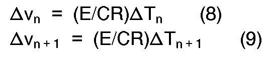
- Fig. 6 illustrates a specific operative example of the
analog subtractor 106. Letting the values ofresistors 501 and 502 be equal to each other and be represented by R1 and the values ofresistors subtractor 106 which are provided therefrom when one of its input voltages △vn and △vn+1 is made zero become as follows:

adder 111 for addition to the output Nn·V0 of theD-A converter 109, they must have the same scale. To this end, the following weighting is required.

- Therefore, the amplification factor R2/Ri that is needed for the
analog subtractor 106 is as follows:
- Thus, each period Pn of successive two input pulses given by expression (1) can be converted, by use of expressions (8), (9), (10) and (14), into the voltage Vn given by the following expression:

- Fig. 7 illustrates a specific operative example of the
adder 111. Letting values ofresistors resistor 603 by R4, the amplification factor of theadder 111 is determined by R4/R3. - Consequently, the result of addition, Vn , of the input signal (AVn - △Vn+1) and the D-A converter output Nn·V0 is provided in the following form:

adder 111 is proportional to the voltage Vn and hence proportional to the period Pn. - In the foregoing description the gate signal shown in Fig. 3K is substantially the same as an inverted version of the signal shown in Fig. 31, and accordingly the Q output of the flip-
flop 125 may also be applied, as a gate signal, directly to the ANDgate 107. In such a case, the ANDgate 123, andOR gate 118, and the flip-flop 126 can be dispensed with. Furthermore, since the output voltage Vn @ obtained in relation to and immediately after the first input pulse (Fig. 3B), that is, an output voltage earlier than Vi in Fig. 3W, may be simply ignored, it is also possible to utilize an arrangement in which the flip-flop 128 and the ANDgate 124 are further omitted and the Q output of the flip-flop 125 is applied directly to the trigger terminal T of themonostable multivibrator 131. - As described above, according to the present invention, the fractional times between the successive input pulses and the clock pulses @ are measured by the pair of fractional
T-V converters over switch 105, the switching operation of which allows thesubtractor 106 to subtract, from the fractional time obtained in relation to any input pulse, the fractional time obtained in relation to the next input pulse. - As a result of this, the fractional times between the input pulses and the clock pulses can be obtained successively, and consequently the voltage signals Vi , V2 , V3 , ... Vn corresponding to the periods Pi, P2, P3, ... Pn each of the successive two input pulses can be yielded in succession at the
output terminal 133. - For example, when an oscilloscope is connected to the
output terminal 133, a voltage waveform corresponding to a variance in the speed of a rotating member can be displayed on the oscilloscope. - When a spectrum analyzer is connected to the
output terminal 133, a frequency analysis can be made of a variance in the speed of the rotating member. Accordingly, a variance in the speed of a rotating machine such as a precision motor or engine can be measured with high precision. - It will be apparent that many modifications and variations may be effected without departing from the scope of the novel concepts of the present invention.
Claims (9)
characterized in that
Applications Claiming Priority (2)
| Application Number | Priority Date | Filing Date | Title |
|---|---|---|---|
| JP62025326A JPH0820473B2 (en) | 1987-02-04 | 1987-02-04 | Continuous period-voltage converter |
| JP25326/87 | 1987-02-04 |
Publications (3)
| Publication Number | Publication Date |
|---|---|
| EP0277638A2 EP0277638A2 (en) | 1988-08-10 |
| EP0277638A3 EP0277638A3 (en) | 1989-08-09 |
| EP0277638B1 true EP0277638B1 (en) | 1992-12-30 |
Family
ID=12162836
Family Applications (1)
| Application Number | Title | Priority Date | Filing Date |
|---|---|---|---|
| EP88101480A Expired - Lifetime EP0277638B1 (en) | 1987-02-04 | 1988-02-02 | Successive period-to-voltage converting apparatus |
Country Status (4)
| Country | Link |
|---|---|
| US (1) | US4769798A (en) |
| EP (1) | EP0277638B1 (en) |
| JP (1) | JPH0820473B2 (en) |
| DE (1) | DE3877008T2 (en) |
Families Citing this family (11)
| Publication number | Priority date | Publication date | Assignee | Title |
|---|---|---|---|---|
| US4870629A (en) * | 1987-01-30 | 1989-09-26 | Hewlett-Packard Company | Method for electronic calibration of a voltage-to-time converter |
| US5132558A (en) * | 1989-01-25 | 1992-07-21 | Hewlett-Packard Co. | Recycling ramp interpolator |
| US5150337A (en) * | 1990-02-21 | 1992-09-22 | Applied Magnetics Corporation | Method and apparatus for measuring time elapsed between events |
| JPH05107287A (en) * | 1991-10-18 | 1993-04-27 | Advantest Corp | Jitter analyzer |
| JPH05273266A (en) * | 1992-03-25 | 1993-10-22 | Advantest Corp | Frequency deviation measuring device |
| JP2583833Y2 (en) * | 1992-10-16 | 1998-10-27 | 株式会社アドバンテスト | Pulse measuring device |
| US5812626A (en) * | 1995-06-13 | 1998-09-22 | Matsushita Electric Industrial Co., Ltd. | Time counting circuit sampling circuit skew adjusting circuit and logic analyzing circuit |
| US6574168B2 (en) | 2000-09-05 | 2003-06-03 | Advantest Corporation | Time measuring device and testing apparatus |
| US7843771B2 (en) * | 2007-12-14 | 2010-11-30 | Guide Technology, Inc. | High resolution time interpolator |
| CN102353837B (en) * | 2011-10-10 | 2013-12-18 | 国电联合动力技术有限公司 | Method and device for measuring pulse frequency |
| US8985849B2 (en) * | 2011-11-11 | 2015-03-24 | Microchip Technology Incorporated | High resolution temperature measurement |
Family Cites Families (7)
| Publication number | Priority date | Publication date | Assignee | Title |
|---|---|---|---|---|
| FR1356389A (en) * | 1963-02-13 | 1964-03-27 | Commissariat Energie Atomique | Time-amplitude converter |
| US3365799A (en) * | 1965-01-13 | 1968-01-30 | Honeywell Inc | Angular position measuring device |
| JPS52123670A (en) * | 1976-04-09 | 1977-10-18 | Takeda Riken Ind Co Ltd | Digital frequency measuring device |
| DE3012186C2 (en) * | 1980-03-28 | 1982-09-23 | MITEC Moderne Industrietechnik GmbH, 8012 Ottobrunn | Timing method and apparatus for its implementation |
| EP0122984B1 (en) * | 1983-04-21 | 1988-08-17 | Hagiwara Denki Kabushiki Kaisha | Time measuring circuit |
| US4504155A (en) * | 1984-03-01 | 1985-03-12 | Chip Supply | Time-to-voltage converter |
| FR2564613B1 (en) * | 1984-05-17 | 1987-04-30 | Commissariat Energie Atomique | HIGH RESOLUTION ELECTRONIC CHRONOMETRY SYSTEM |
-
1987
- 1987-02-04 JP JP62025326A patent/JPH0820473B2/en not_active Expired - Fee Related
-
1988
- 1988-02-01 US US07/151,181 patent/US4769798A/en not_active Expired - Lifetime
- 1988-02-02 DE DE8888101480T patent/DE3877008T2/en not_active Expired - Fee Related
- 1988-02-02 EP EP88101480A patent/EP0277638B1/en not_active Expired - Lifetime
Also Published As
| Publication number | Publication date |
|---|---|
| US4769798A (en) | 1988-09-06 |
| EP0277638A3 (en) | 1989-08-09 |
| DE3877008T2 (en) | 1993-05-13 |
| DE3877008D1 (en) | 1993-02-11 |
| JPS63191970A (en) | 1988-08-09 |
| EP0277638A2 (en) | 1988-08-10 |
| JPH0820473B2 (en) | 1996-03-04 |
Similar Documents
| Publication | Publication Date | Title |
|---|---|---|
| US4569599A (en) | Method of determining the difference between the transit times of measuring pulse signals and reference pulse signals | |
| US4112358A (en) | Digital frequency measuring device | |
| EP0234883B1 (en) | Apparatus and method for random repetitive sampling | |
| US3983481A (en) | Digital intervalometer | |
| USRE32845E (en) | Period and frequency measuring instrument | |
| US4769798A (en) | Successive period-to-voltage converting apparatus | |
| US5200933A (en) | High resolution data acquisition | |
| JP3434095B2 (en) | Frequency measuring device | |
| US4637733A (en) | High-resolution electronic chronometry system | |
| US4870664A (en) | Continuous counting device | |
| US4267436A (en) | Interval-expanding timer compensated for drift and nonlinearity | |
| NL8004816A (en) | A / D CONVERTER. | |
| GB2144935A (en) | Device for measuring the time between two events | |
| US3943341A (en) | Computing apparatus | |
| JPH07280857A (en) | Pulse width measurement circuit | |
| US4523288A (en) | Interval-expanding timer | |
| EP0662755A1 (en) | Ramp generator | |
| KR950000418B1 (en) | Pulse width measurement with quantisation error compensation | |
| SU1328762A1 (en) | Digital phase meter of instantaneous values | |
| SU966660A1 (en) | Device for measuring short pulse duration | |
| SU1522401A1 (en) | Device for measuring dynamic parameters of fast a-d converters | |
| JPH0333013Y2 (en) | ||
| SU377798A1 (en) | ALL-UNION | |
| JPH0455275B2 (en) | ||
| JPH03235527A (en) | A/d converter |
Legal Events
| Date | Code | Title | Description |
|---|---|---|---|
| PUAI | Public reference made under article 153(3) epc to a published international application that has entered the european phase |
Free format text: ORIGINAL CODE: 0009012 |
|
| 17P | Request for examination filed |
Effective date: 19880202 |
|
| AK | Designated contracting states |
Kind code of ref document: A2 Designated state(s): DE GB NL |
|
| PUAL | Search report despatched |
Free format text: ORIGINAL CODE: 0009013 |
|
| RHK1 | Main classification (correction) |
Ipc: G04F 10/00 |
|
| AK | Designated contracting states |
Kind code of ref document: A3 Designated state(s): DE GB NL |
|
| 17Q | First examination report despatched |
Effective date: 19910318 |
|
| GRAA | (expected) grant |
Free format text: ORIGINAL CODE: 0009210 |
|
| AK | Designated contracting states |
Kind code of ref document: B1 Designated state(s): DE GB NL |
|
| REF | Corresponds to: |
Ref document number: 3877008 Country of ref document: DE Date of ref document: 19930211 |
|
| PLBE | No opposition filed within time limit |
Free format text: ORIGINAL CODE: 0009261 |
|
| STAA | Information on the status of an ep patent application or granted ep patent |
Free format text: STATUS: NO OPPOSITION FILED WITHIN TIME LIMIT |
|
| 26N | No opposition filed | ||
| PGFP | Annual fee paid to national office [announced via postgrant information from national office to epo] |
Ref country code: GB Payment date: 19940126 Year of fee payment: 7 |
|
| PGFP | Annual fee paid to national office [announced via postgrant information from national office to epo] |
Ref country code: NL Payment date: 19940228 Year of fee payment: 7 |
|
| PG25 | Lapsed in a contracting state [announced via postgrant information from national office to epo] |
Ref country code: GB Effective date: 19950202 |
|
| PG25 | Lapsed in a contracting state [announced via postgrant information from national office to epo] |
Ref country code: NL Effective date: 19950901 |
|
| GBPC | Gb: european patent ceased through non-payment of renewal fee |
Effective date: 19950202 |
|
| NLV4 | Nl: lapsed or anulled due to non-payment of the annual fee |
Effective date: 19950901 |
|
| PGFP | Annual fee paid to national office [announced via postgrant information from national office to epo] |
Ref country code: DE Payment date: 19960226 Year of fee payment: 9 |
|
| PG25 | Lapsed in a contracting state [announced via postgrant information from national office to epo] |
Ref country code: DE Effective date: 19971101 |