EP0273081B1 - Improved duplicated circuit arrangement for fast transmission and repairability - Google Patents
Improved duplicated circuit arrangement for fast transmission and repairability Download PDFInfo
- Publication number
- EP0273081B1 EP0273081B1 EP86430056A EP86430056A EP0273081B1 EP 0273081 B1 EP0273081 B1 EP 0273081B1 EP 86430056 A EP86430056 A EP 86430056A EP 86430056 A EP86430056 A EP 86430056A EP 0273081 B1 EP0273081 B1 EP 0273081B1
- Authority
- EP
- European Patent Office
- Prior art keywords
- processing element
- main processor
- bits
- bus
- drivers
- Prior art date
- Legal status (The legal status is an assumption and is not a legal conclusion. Google has not performed a legal analysis and makes no representation as to the accuracy of the status listed.)
- Expired - Lifetime
Links
Images

Classifications
-
- G—PHYSICS
- G06—COMPUTING OR CALCULATING; COUNTING
- G06F—ELECTRIC DIGITAL DATA PROCESSING
- G06F11/00—Error detection; Error correction; Monitoring
- G06F11/07—Responding to the occurrence of a fault, e.g. fault tolerance
- G06F11/16—Error detection or correction of the data by redundancy in hardware
Definitions
- the present invention relates to the transmission of digital data signals on electrical busses and more particularly to an improved duplicated circuit arrangement wherein the number of simultaneous switches in the redundant devices is significantly reduced.
- circuit duplication is a method often used to detect failures in systems where a high confidence level in failure detection is required.
- two identical processing elements perform the same operations on the same data, their results are continuously compared, and a failure is detected if they do not match.
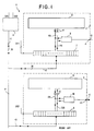
- Fig. 1 illustrates a known circuit arrangement of the prior art referenced 1 in the drawing, which embodies duplicated hardware. It will be used to set forth the problems raised by the simultaneous switching of output drivers when a duplicated circuit is implemented in a system. It is assumed that devices 2 and 3 are identical and therefore perform the same operation (when not defective) under the control of the main processor 4. Devices 2 and 3 may be for example, the floating point co-processor chip described in an article entitled:" Custom floating point chip designed with a cohesive structured method" by B. Desrosiers et al, published in the proceedings of the IEEE International Conference on Computer Design: VLSI in Computers ICCD'86 pp 402-405.
- device 2 is considered the master and device 3, the slave.
- Each device (2;3) is comprised of a processing element (5;6), working on a P bit word, for example, thirty six bits or four bytes, a send/receive circuit (7;8) and a compare circuit (9;10) respectively.
- a processing element for example, thirty six bits or four bytes
- a send/receive circuit for example, thirty six bits or four bytes
- a compare circuit 9;10 respectively.
- An example of an appropriate processing element is shown in Fig. 1 of the above mentioned article.
- Send/receive circuits 7 and 8 assure transmission of the four bytes (thirty two bits of data plus four parity bits) to and from the main data bus 11 of main processor 4, through bidirectional busses 12 and 13 respectively. Busses 12 and 13 are referenced to the device data bus, to be distinguished from the main processor data bus, referenced to the main data bus. However, it is to be noted that send/receive circuit 8 functionally operates only as a receiver in normal operation. Send/receive circuits 7 and 8 also assure bidirectional transmission of the P bit word to and from processing elements 5 and 6 on, busses 14 and 15 respectively.
- Send/receive circuits 7 and 8 are comprised of a plurality of basic units, one per bit. Each unit is constituted of a separate output driver and receiver, having the output of the driver and the input of the receiver forming a common node connected to a line of the bus. Standard three state drivers and receivers are used for that application. An on-chip tristate driver is depicted in an article of the IBM Technical Disclosure Bulletin Vol. 25, No.5, October 1982, pages 2347-2348. The high impedance state of the drivers forming parts of send/receive circuits 7 and 8 is under the control of main processor 4 through control (inhibit) lines SR1 and SR2.
- Compare circuit 9 which compares the bytes available on bus 14A after processing in processing element 5 with the bytes available on bus 14B, received from bus 12, is of no real utility in normal operation in the sense that it is not used to compare the validity of data after processing in the two processing elements, but it is of some interest since it may check the integrity of the send/receive circuit (drivers and receivers).
- Bus 14A is an unidirectional bus which connects the outputs of processing element 5 to the inputs of the drivers of send/receive circuits 7.
- Bus 14B is an unidirectional bus which connects the inputs of processing element 5 to the outputs of receivers of send/receive circuit 7.
- Busses 14A and 14B form the internal bus 14 of device 2.
- Compare circuit 10 compares the bytes processed by processing element 6 available on bus 15A with bytes received from device 2 and available on bus 15B.
- Bus 15A is an unidirectional bus which connects the outputs of processing element 6 to the inputs of drivers of send/receive circuit 8.
- Bus 15B is an unidirectional bus which connects the inputs of processing element 6 to the outputs of the receivers of send/receive circuit 8.
- Busses 15A and 15B form the internal bus 15 of device 3.
- the output of compare circuit 10 at node 16 provides the check out (CHKOUT) bit on line 17 for the main processor 4.
- the corresponding send/receive circuit is said to be in the SEND mode, and so is the corresponding device.
- the corresponding send/receive circuit When all the drivers are inhibited, they are in the high impedance state, the corresponding send/receive circuit is said to be in the RECEIVE mode, and so is the corresponding device.
- the operation takes place in three steps:
- device 3 (the slave) is used only for checking purposes while device 2 (the master) assures the data exchange with the main processor 4.
- the main processor stops the task in progress and starts a diagnostic routine to determine which one of the two devices (in fact which processing element) is the failing one.
- the good device is then switched to operate as the master while the failing one is disabled (output drivers forced into the high impedance state). Processing can then continue in a degraded operation without the previous checking capability until repair.
- device 2 may be an integrated semiconductor chip or an electronic module and during the TRANSMISSION step where bits are transmitted on data bus 12, it may happen that a majority, if not all the P (e.g. thirty six) drivers forming the emitting portion of the send/receive circuit 7, may switch simultaneously, therefore producing the above-mentioned undesirable noise effects.
- P e.g. thirty six
- a 4 byte wide bidirectional data bus 11 has been chosen to illustrate this proposal but any other configuration can be used: unidirectional busses or busses of different width.
- an improved circuit arrangement including a plurality of redundant devices for data transmission wherein the driving effort of the redundant devices on the data bus is shared between said devices.
- the driving effort is equally shared between the N devices to divide by a factor N the maximum number of simultaneous switches for each device. As a result, this significantly improves the data transmission speed on said data bus.
- an improved circuit arrangement of redundant devices including a main processor provided with a P bit data bus, N redundant devices; each of which device includes a processing element, processing a P bit word or frame and receiving means connected between the outputs of the processing element and the lines of the device data bus, the latter being mounted in parallel with said P bit main data bus.
- Driving means controlled by the main processor are provided to at least two of the N redundant devices to share the driving effort on the P bit main data bus between them so that they each transmit only a part of the P bit word, while the latter is wholly available on said P bit data bus.
- the word is split into a series of consecutive sets or segments of bits, each corresponding to a particular section of the processing element; each device will emit only its own set of P/N bits on the data bus of the main processor.
- the first device emits the first set of bits ranking from 1 to I
- the second device emits the second set of bits ranking from I+1 to J
- the Nth device emits the last set of bits ranking from K+1 to P.
- any device may emit any set of bits, it is only necessary that each set of bits is emitted once and the P bit word is emitted in integrality.
- the maximum number of simultaneous switching for each device is divided by N, and is now equal to P/N.
- said driving means consists of at least one group of drivers dedicated to a particular section of the processing element.
- said driving means consists of one group of drivers dedicated to any section of the processing element and multiplexors, to properly orient the content of the appropriate section of the processing element to be sent.
- an improved circuit arrangement of N redundant devices which allows increased information transmission rate.
- the driving effort on the data bus is equally shared between said devices.
- the maximum number of simultaneous switching for each device is divided by N.
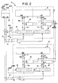
- Arrangement 20 is basically comprised of devices 21 and 22 which are assumed to be identical.
- Device 21 includes a processing element 23 working on a P bit word, say thirty six bits or four bytes, two send/receive circuits 24 and 25, and two compare circuits 26 and 27 (which may be either on or off chip but preferably on chip to limit external switchings).
- Processing element 23 is considered to be comprised of two sections, each of P/2 bits.
- the MSB section handles the MSB's (Most Significant Bits) and the LSB section handles the LSB's (Less Significant Bits).
- Send/receive circuits 24 and 25 assure transmission of the MSB's and LSB's to and from processing element 23 on busses 28 and 29 respectively, and assure a bidirectional transmission with the main processor 30 respectively, via busses 31 and 32 which are connected in parallel with busses 33 and 34 of the main processor 30.
- send/receive circuit 24 handles the Most Significant Bits (MSB's)
- send/receive circuit 25 handles the Less Significant Bits (LSB's). Same reasoning applies to device 22.
- device 22 includes a processing element 35 working also on four bytes, two send/receive circuits 36 and 37, and two compare circuits 38 and 39.
- Send/receive circuits 36 and 37 assure transmission of the MSB's and LSB's to and from processing element 35 on bus 40 and 41 respectively and assure a bidirectional transmission with the main processor 30, respectively via busses 42 and 43 which are connected in parallel with busses 33 and 34 of the main processor.
- Busses 33 and 34 constitute the data bus 44 of the main processor.
- Compare circuit 27 compares the LSB's generated by processing element 23 and available on bus 29A with LSB's processed by processing element 35 and available on bus 29B at the output of send/receive circuit 25.
- Compare circuit 26 has no real utility as long as device 21 properly functions.
- compare circuit 38 compares the MSB's generated by processing element 35 and available on bus 40A with MSB's elaborated by processing element 23 and available on bus 40B at the output of send/receive circuit 36. The output of all compare circuits are AND dotted at node 45 and provide the CHKOUT bit on line 46 for the main processor 30.
- Compare circuit 39 like compare circuit 26 is of no utility in this particular configuration but could be used in others.
- Send/receive circuits are operating in either one of two modes: RECEIVE or SEND, under the control of the main processor 30 through control lines SR 11, SR 12, SR 21 and SR 22. If necessary, the main processor may also receive the parity bits from the parity bit generator (not shown). Busses 31 and 32 constitute data bus 47 of device 21 and busses 42 and 43 constitute data bus 48 of device 22.
- Fig. 2 clearly shows how the concept of the present invention can be applied to the known duplicated circuit arrangement described above with respect to Fig. 1.
- the original send/receive and compare circuits of Fig. 1 have been split into two parts corresponding to two sections of the processing element identified as MSB and LSB sections.
- the send/receive control lines have been doubled in order to allow separate controls on MSB's and LSB's of both devices via SR11, SR12, SR21, and SR22.
- Both devices 21 and 22 are each comprised of two identical halves each corresponding to a determined section of the processing element.
- each device sends its own set of bits (e.g. MSB's for device 21 and LSB's for device 22), to the main processor, and half of each device 21 and 22 operates in different modes.
- the first half (which handles the MSB's) is in the SEND mode while the other half (which handles the LSB's) is in the RECEIVE/COMPARE mode.
- the first half is in the RECEIVE/COMPARE mode while the other half is in the SEND mode. All these elementary consecutive sets are reassembled to form the complete set of P bits on the data bus (e.g.44).
- the main processor to appropriately select the good section of either device to fictitiously reconstruct a functionally operating device, when one device has a failure on one section, as it will be detailed hereafter.
- Main processor 30 stops the task in progress and starts a diagnosis routine to identify which one of the two processing element 23 and 35 is defective, and then which section of it is defective (MSB or LSB). Then it takes corrective actions to reconfigure the task according to the diagnostic results.
- the defective half of the device is disabled.
- the corresponding output drivers are set in the high impedance state and the corresponding compare circuit is inhibited and thus by forcing its output at a high impedance state, it avoids invalidation of the CHKOUT bit.
- This defective half is in a particular variant of the RECEIVE mode, so called HIGH IMPEDANCE mode to distinguish from the RECEIVE/COMPARE mode.
- the other half is set to the SEND mode.
- the additional set of bits being provided to the main processor by the other device. Processing can continue at same data rate but checking is lost on half of the bits.
- both sections of a processing element of device are defective, said device is fully disabled by forcing all the drivers of the send/receive circuits in the high impedance state and by inhibiting the compare circuits if so desired. And processing continues with the other device at reduced speed and with no checking at all.
- the device is said to operate in the HIGH IMPEDANCE mode. In this mode, the main processor cannot test the CHKOUT bit because it is permanently invalid.
- the system is now operating in the so called “degraded operation”.
- Speed must be reduced because of simultaneous switching constraints as explained above. This can be done as known in the art, by staggering the SEND commands of MSB's with respect to LSB's or by generating two gating signals internally to the device, starting from a unique clock signal. For instance, the pulse position shift can simply be a cycle time, thus dividing the data rate by two, or can be adjusted to the minimal amount imposed by the technology wiring rules. In this last case the performance loss is minimized but clocking circuitry may be more complex.
- TABLE 1 shows the tasks allocated by the main processor 30 to devices 21 and 22 through the different operating modes of device halves during the TRANSMISSION step, depending on which section of the processing element (P.E.) the failure is located.
- device 21 and 22 may be simplified in some respects, if one accepts to limit the system capabilities (in some cases such a limitation may be unacceptable for the system designer).
- device 21 only sends data via bus 31 and device 22 only sends data via bus 43 to the main processor.
- Each device needs compare circuitry for two bytes only (P/2 bits). Compare circuits 26 and 39 may be eliminated if so desired.
- half of the send/receive circuits operate only in the RECEIVE/COMPARE mode during the TRANSMISSION step. As a result, relatively complex send/receive comprised of both drivers and receivers units may be simply replaced by standard receivers.
- the duplicated circuit arrangement 50 shown in Fig. 3 is basically comprised of devices 51 and 52 which are still assumed to be identical.
- Device 51 includes a processing element 53 working, for instance, on a P bit word (e.g. four bytes), one send/receive circuit 54, one receive circuit 55, one compare circuit 56 and lastly a multiplexor 57.
- Processing element 53 is still comprised of two sections, each of P/2 bits.
- the MSB section handles the MSB's (Most Significant Bits) and the LSB section handles the LSB's (Less Significant Bits).
- Send/receive circuit 54 assures bidirectional transmission of the MSB's or the LSB's to and from processing element 52, on bus 58 and on either bus 59 or 60.
- send/receive circuit 54 assures a bidirectional transmission with the main processor 61 via bus 62 which is connected in parallel with bus 63 of the main processor 61.
- bus 63 handles either the MSB's or the LSB's.
- the selection between the MSB's or the LSB's to be sent by send/receive circuit 54 is made by multiplexor 57 under control of the main processor 61 through control line M1.
- the send/receive circuit 54 operates either in the SEND mode or in the RECEIVE mode under the control of the main processor 61 through control line SR13. It operates in the RECEIVE mode when the drivers are set in the high impedance state.
- Receive circuit 55 receives data (either the MSB's or the LSB's) from data busses 64 and 65 and transmits them to the processing element 53 first through bus 66A then through either bus 59 or through bus 60 depending the action of multiplexor 57.
- Compare circuit 56 compares the data (MSB's or LSB's) generated by processing element 53 on its internal bus 66B with corresponding data generated by the processing element of device 52 available on bus 66B.
- Busses 62 and 65 constitute data bus 67 of device 51.
- Device 52 is structurally identical to device 51.
- Device 52 includes a processing element 68, one send/receive circuit 69, one receive circuit 70, one compare circuit 71 and lastly a multiplexor 72.
- Send/receive circuit 69 assures bidirectional transmission of the MSB's or the LSB's to and from processing element 68, on bus 73 and either bus 74 or 75.
- send/receive circuit 69 assures a bidirectional transmission with the main processor 61 via bus 76 which is connected in parallel with bus 64 of the main processor 61.
- the selection between the MSB's or the LSB's to be sent by send/receive circuit 69 is made by multiplexor 72 under control of the main processor 61 through control line M2.
- the send/receive circuit 69 operates either in the SEND mode or, in the RECEIVE mode, under the control of the main processor 61 through control line SR23.
- Receive circuit 70 receives data (either the MSB's or the LSB's) from data busses 63 and 77 and transmits them to the processing element 68 first through bus 78A then either through bus 74 or 75 depending the action of multiplexor 72.
- Compare circuit 71 compares the data (MSB's or LSB's) generated by processing element 68 on an internal bus 78B with corresponding data generated by processing element 53 of device 51 available on bus 78A.
- Busses 76 and 77 constitute bus 79 of device 52.
- the outputs of compare circuits 56 and 71 are AND dotted at node 80 and provide the CHKOUT bit on line 81 for the main processor 61.
- Halves of devices 51 and 52 are no longer symmetrical.
- main processor 61 there is also a multiplexor referenced 82.
- Data busses 63 and 64 constitute the main data bus 83 of the main processor.
- This latter step constitutes the TRANSMISSION step of the system.
- Any miscompare detection is sent to the main processor 61 that stops the task in progress and starts a diagnosis routine to detect which one of the two processing element has a failure and which part or section (MSB or LSB) of it is concerned. Then it takes corrective action to reconfigure the task according to the diagnostic results.
- send/receive circuit e.g. 54
- compare circuit e.g. 56
- the send/receive circuit operates in a so called S seq S mode, to indicate that LSB section and MSB section are sequentially connected to the send/receive circuit by shifted clock pulses. Adequate multiplexing also takes place in the main processor since only one half of bus 83 is used to transmit data.
- TABLE 2 shows the tasks allocated by the main processor 61 to devices 51 and 52 through the operating modes of send/receive circuits and multiplexors during the TRANSMISSION step, depending on the section of the processing element (P.E.) where the failure is located.
- this proposal is even more efficient when N is larger than 2, say 3 in a typical implementation of a majority voting check circuit arrangement.
- the number of simultaneous switchings is alleviated by a bigger amount and the detection of the failing device is made simpler and faster.
Landscapes
- Engineering & Computer Science (AREA)
- Theoretical Computer Science (AREA)
- Quality & Reliability (AREA)
- Physics & Mathematics (AREA)
- General Engineering & Computer Science (AREA)
- General Physics & Mathematics (AREA)
- Hardware Redundancy (AREA)
- Bus Control (AREA)
Description
- The present invention relates to the transmission of digital data signals on electrical busses and more particularly to an improved duplicated circuit arrangement wherein the number of simultaneous switches in the redundant devices is significantly reduced. In addition, according to the invention, it is possible to select only the operative sections of said devices to continue processing.
- On the one hand, circuit duplication is a method often used to detect failures in systems where a high confidence level in failure detection is required. In accordance with such a method, two identical processing elements perform the same operations on the same data, their results are continuously compared, and a failure is detected if they do not match.
- On the other hand, it is also well known that the data transmission rate between chips or modules on electrical busses is restricted by certain limitations related to the maximum number of simultaneously switching output drivers allowed. These limitations are due to voltage or current noises induced into the voltage distribution and signal lines when output drivers are simultaneously driving a large number of data bus lines. Known solutions are accompanied by heavy penalties in terms of packaging development and cost: complex voltage distribution, complicated line drivers and receivers, reduced bus width, as well as in terms of machine speed because it results in slower signal transmission due to the necessity of using controlled delayed transients in order to avoid the said phenomena of simultaneous switching.
- Fig. 1 illustrates a known circuit arrangement of the prior art referenced 1 in the drawing, which embodies duplicated hardware. It will be used to set forth the problems raised by the simultaneous switching of output drivers when a duplicated circuit is implemented in a system. It is assumed that
devices Devices device 2 is considered the master anddevice 3, the slave. Each device (2;3) is comprised of a processing element (5;6), working on a P bit word, for example, thirty six bits or four bytes, a send/receive circuit (7;8) and a compare circuit (9;10) respectively. An example of an appropriate processing element is shown in Fig. 1 of the above mentioned article. - Send/receive
circuits main data bus 11 of main processor 4, throughbidirectional busses 12 and 13 respectively.Busses 12 and 13 are referenced to the device data bus, to be distinguished from the main processor data bus, referenced to the main data bus. However, it is to be noted that send/receivecircuit 8 functionally operates only as a receiver in normal operation. Send/receivecircuits processing elements - Send/receive
circuits circuits - Compare
circuit 9, which compares the bytes available onbus 14A after processing inprocessing element 5 with the bytes available on bus 14B, received frombus 12, is of no real utility in normal operation in the sense that it is not used to compare the validity of data after processing in the two processing elements, but it is of some interest since it may check the integrity of the send/receive circuit (drivers and receivers).Bus 14A is an unidirectional bus which connects the outputs ofprocessing element 5 to the inputs of the drivers of send/receivecircuits 7. Bus 14B is an unidirectional bus which connects the inputs ofprocessing element 5 to the outputs of receivers of send/receivecircuit 7.Busses 14A and 14B form the internal bus 14 ofdevice 2. Compare circuit 10 compares the bytes processed byprocessing element 6 available onbus 15A with bytes received fromdevice 2 and available onbus 15B.Bus 15A is an unidirectional bus which connects the outputs ofprocessing element 6 to the inputs of drivers of send/receivecircuit 8.Bus 15B is an unidirectional bus which connects the inputs ofprocessing element 6 to the outputs of the receivers of send/receivecircuit 8.Busses device 3. The output of compare circuit 10 at node 16 provides the check out (CHKOUT) bit online 17 for the main processor 4. - When all the drivers are not inhibited, the corresponding send/receive circuit is said to be in the SEND mode, and so is the corresponding device.
- When all the drivers are inhibited, they are in the high impedance state, the corresponding send/receive circuit is said to be in the RECEIVE mode, and so is the corresponding device.
- The operation takes place in three steps:
- a) Main processor 4 sets send/receive
circuits devices busses - b) Both
processing elements devices - c) Main processor 4 sets send/receive
circuit 7 ofdevice 2 to the SEND mode and send/receivecircuit 8 ofdevice 3 to the RECEIVE mode. Because when settled in the RECEIVE mode during this step, the send/receive circuit will also allow the compare function. This operating mode of the send/receive circuit will be referenced as the RECEIVE/COMPARE mode. This particular step is called the TRANSMISSION step. Send/receivecircuit 7 ofdevice 2 transmits the processed data to the main processor 4 and todevice 3 throughbusses device 3 compares its own internal results available onbus 15A with the data received fromdevice 2 available onbus 15B and sends the comparison result to the main processor via output node 16 andline 17. The output of comparecircuit 9 is available atnode 18 and line 19, but has the limited use mentioned in the above operation. - Therefore, in normal operation, device 3 (the slave) is used only for checking purposes while device 2 (the master) assures the data exchange with the main processor 4.
- However, in case of mismatch the main processor stops the task in progress and starts a diagnostic routine to determine which one of the two devices (in fact which processing element) is the failing one. The good device is then switched to operate as the master while the failing one is disabled (output drivers forced into the high impedance state). Processing can then continue in a degraded operation without the previous checking capability until repair.
- There is no means of selecting the operative sections of the processing elements of any devices while maintaining some checking capability.
- The duplicated circuit arrangement of two redundant devices shown in Fig. 1, has still another, but primary, disadvantage:
device 2 may be an integrated semiconductor chip or an electronic module and during the TRANSMISSION step where bits are transmitted ondata bus 12, it may happen that a majority, if not all the P (e.g. thirty six) drivers forming the emitting portion of the send/receivecircuit 7, may switch simultaneously, therefore producing the above-mentioned undesirable noise effects. - To date, the only known way of reducing that phenomenon of simultaneous switching is to properly use controlled delayed transients at the cost of an important reduction of the data transmission speed.
- A 4 byte wide
bidirectional data bus 11 has been chosen to illustrate this proposal but any other configuration can be used: unidirectional busses or busses of different width. - Because, as new semiconductor technologies arise, there is a continuous effort in developing circuits and applications involving both redundant devices, wide data busses (such as handling 64 or 128 bits) and operating at very high frequency. As a result, there is still an obvious need for an improved circuit arrangement of two redundant devices alleviating all the problems related to the simultaneous switching of output drivers mentioned above.
- Therefore it is the object of the present invention to provide an improved circuit arrangement of redundant devices wherein each of the interconnected redundant devices exhibits reduced simultaneous switching for speed improvement and packaging cost reduction.
- It is an aspect of the present invention to provide an improved circuit arrangement of redundant devices which allows the selection of the operative sections of the processing elements of any interconnected redundant devices to provide a good overall functioning of the system and a high level of reliability and repairability.
- It is still a further aspect of the present invention to provide an improved circuit arrangement of redundant devices which still has a degraded operation to allow the only operative device to continue processing by itself when the others have fully failed.
- According to its most general principle, there is provided an improved circuit arrangement including a plurality of redundant devices for data transmission wherein the driving effort of the redundant devices on the data bus is shared between said devices. Preferably, the driving effort is equally shared between the N devices to divide by a factor N the maximum number of simultaneous switches for each device. As a result, this significantly improves the data transmission speed on said data bus.
- According to that general principle, there is provided an improved circuit arrangement of redundant devices, including a main processor provided with a P bit data bus, N redundant devices; each of which device includes a processing element, processing a P bit word or frame and receiving means connected between the outputs of the processing element and the lines of the device data bus, the latter being mounted in parallel with said P bit main data bus. Driving means controlled by the main processor are provided to at least two of the N redundant devices to share the driving effort on the P bit main data bus between them so that they each transmit only a part of the P bit word, while the latter is wholly available on said P bit data bus.
- In other words, if the processing elements are handling a frame or a word of P bits, the word is split into a series of consecutive sets or segments of bits, each corresponding to a particular section of the processing element; each device will emit only its own set of P/N bits on the data bus of the main processor. For example, the first device emits the first set of bits ranking from 1 to I, the second device emits the second set of bits ranking from I+1 to J, ... and the Nth device emits the last set of bits ranking from K+1 to P. However any device may emit any set of bits, it is only necessary that each set of bits is emitted once and the P bit word is emitted in integrality. As a result, the maximum number of simultaneous switching for each device is divided by N, and is now equal to P/N.
- According to a first preferred embodiment as claimed in
claim 1, said driving means consists of at least one group of drivers dedicated to a particular section of the processing element. - According to another preferred embodiment as claimed in
claim 5, said driving means consists of one group of drivers dedicated to any section of the processing element and multiplexors, to properly orient the content of the appropriate section of the processing element to be sent. - However, the most common case is when hardware duplication is used (N=2).
- The objects and features of the present invention will become more apparent after considering the following detailed description taken in conjunction with the accompanying drawings in which:
- Fig. 1 shows a duplicated circuit arrangement of the prior art, according to which, one of the redundant devices is used only for check purposes, the other having a maximum sensitivity to the simultaneous switching problems.
- Fig. 2 shows an improvement to the duplicated circuit arrangement of Fig. 1 in accordance with the present invention, wherein said simultaneous switching problem is significantly reduced, and the selection of the operative sections of any redundant device is allowed.
- Fig. 3 shows an alternative of the duplicated circuit arrangement of Fig. 2.
- According to the basic principle of the invention, it is suggested an improved circuit arrangement of N redundant devices which allows increased information transmission rate. Preferably, the driving effort on the data bus is equally shared between said devices. As a result, the maximum number of simultaneous switching for each device is divided by N.
- Because the most simple case is hardware duplication (N=2), it has been chosen for illustration purposes. The invention is based on the fact that the devices always perform the same operations when they are not defective. Sharing the bus driving effort between the two devices alleviates the simultaneous switching constraints and improves the system "cost X performance" product.
- The improved duplicated circuit arrangement according to the present invention, is referenced 20 in Fig. 2.
Arrangement 20 is basically comprised ofdevices Device 21 includes aprocessing element 23 working on a P bit word, say thirty six bits or four bytes, two send/receivecircuits circuits 26 and 27 (which may be either on or off chip but preferably on chip to limit external switchings). Processingelement 23 is considered to be comprised of two sections, each of P/2 bits. The MSB section handles the MSB's (Most Significant Bits) and the LSB section handles the LSB's (Less Significant Bits). Send/receivecircuits element 23 onbusses main processor 30 respectively, viabusses 31 and 32 which are connected in parallel withbusses main processor 30. In others words, fordevice 21, send/receivecircuit 24 handles the Most Significant Bits (MSB's), and send/receivecircuit 25 handles the Less Significant Bits (LSB's). Same reasoning applies todevice 22. - Similarly
device 22 includes aprocessing element 35 working also on four bytes, two send/receivecircuits circuits - Send/receive
circuits element 35 onbus main processor 30, respectively viabusses busses Busses data bus 44 of the main processor. - Compare
circuit 27 compares the LSB's generated by processingelement 23 and available onbus 29A with LSB's processed by processingelement 35 and available onbus 29B at the output of send/receivecircuit 25. Comparecircuit 26 has no real utility as long asdevice 21 properly functions. Similarly, comparecircuit 38 compares the MSB's generated by processingelement 35 and available onbus 40A with MSB's elaborated by processingelement 23 and available onbus 40B at the output of send/receivecircuit 36. The output of all compare circuits are AND dotted atnode 45 and provide the CHKOUT bit online 46 for themain processor 30. Comparecircuit 39, like comparecircuit 26 is of no utility in this particular configuration but could be used in others. Send/receive circuits are operating in either one of two modes: RECEIVE or SEND, under the control of themain processor 30 throughcontrol lines SR 11,SR 12,SR 21 andSR 22. If necessary, the main processor may also receive the parity bits from the parity bit generator (not shown).Busses 31 and 32 constitutedata bus 47 ofdevice 21 and busses 42 and 43 constitutedata bus 48 ofdevice 22. - Thus, Fig. 2 clearly shows how the concept of the present invention can be applied to the known duplicated circuit arrangement described above with respect to Fig. 1. For each device, the original send/receive and compare circuits of Fig. 1 have been split into two parts corresponding to two sections of the processing element identified as MSB and LSB sections. The send/receive control lines have been doubled in order to allow separate controls on MSB's and LSB's of both devices via SR11, SR12, SR21, and SR22. Both
devices - The improved duplicated circuit arrangement of Fig. 2 operates as follows:
- a) Main processor sets send/receive
circuits device 21 and send/receivecircuits device 22 to RECEIVE mode, and sends them the data to be processed. - b)
Processing elements - c)
Main processor 30 sets the send/receivecircuit 24 ofdevice 21 and send/receivecircuit 37 ofdevice 22 to SEND mode; conversely, it sets send/receivecircuit 25 ofdevice 21 and send/receivecircuit 36 ofdevice 22 to RECEIVE mode. Because, when set in the RECEIVE mode in this step, the send/receive circuit will also allow the compare function, this mode will be referenced as to the RECEIVE/COMPARE mode. During this step,device 21 sends MSB's tomain processor 30 and todevice 22, and compares its own LSB's with LSB's received fromdevice 22. Simultaneously,device 22 sends LSB's tomain processor 30 and todevice 21, and compares its own MSB's with MSB's received fromdevice 21. - This particular operation characterizes the TRANSMISSION step where each device sends its own set of bits (e.g. MSB's for
device 21 and LSB's for device 22), to the main processor, and half of eachdevice device 21, the first half (which handles the MSB's) is in the SEND mode while the other half (which handles the LSB's) is in the RECEIVE/COMPARE mode. Fordevice 22, the first half is in the RECEIVE/COMPARE mode while the other half is in the SEND mode. All these elementary consecutive sets are reassembled to form the complete set of P bits on the data bus (e.g.44). - According to a first aspect of the invention, there is a significant reduction of the maximum number of simultaneous switches. This number, either for
device 21 or fordevice 22, is now equal to P/2, for instance, eighteen in the present example compared to thirty six fordevice 2 in the example depicted in Fig. 1. It is clear that the driving effort now equally shared between the two devices allows that reduction. - According to another aspect of the invention for better reliability and repairability, there is also an opportunity for the main processor to appropriately select the good section of either device to fictitiously reconstruct a functionally operating device, when one device has a failure on one section, as it will be detailed hereafter.
- If a mismatch is detected by any one of the two compare
circuits main processor 30 vianode 45 online 46.Main processor 30 stops the task in progress and starts a diagnosis routine to identify which one of the twoprocessing element - If only one section of a processing element is defective, the defective half of the device is disabled. The corresponding output drivers are set in the high impedance state and the corresponding compare circuit is inhibited and thus by forcing its output at a high impedance state, it avoids invalidation of the CHKOUT bit. This defective half is in a particular variant of the RECEIVE mode, so called HIGH IMPEDANCE mode to distinguish from the RECEIVE/COMPARE mode. The other half is set to the SEND mode. The additional set of bits being provided to the main processor by the other device. Processing can continue at same data rate but checking is lost on half of the bits.
- If both sections of a processing element of device are defective, said device is fully disabled by forcing all the drivers of the send/receive circuits in the high impedance state and by inhibiting the compare circuits if so desired. And processing continues with the other device at reduced speed and with no checking at all. The device is said to operate in the HIGH IMPEDANCE mode. In this mode, the main processor cannot test the CHKOUT bit because it is permanently invalid. The system is now operating in the so called "degraded operation". Speed must be reduced because of simultaneous switching constraints as explained above. This can be done as known in the art, by staggering the SEND commands of MSB's with respect to LSB's or by generating two gating signals internally to the device, starting from a unique clock signal. For instance, the pulse position shift can simply be a cycle time, thus dividing the data rate by two, or can be adjusted to the minimal amount imposed by the technology wiring rules. In this last case the performance loss is minimized but clocking circuitry may be more complex.
- TABLE 1 shows the tasks allocated by the
main processor 30 todevices 

- However, as it may be understood from Fig. 2 and TABLE 1, the design of
devices device 21 only sends data via bus 31 anddevice 22 only sends data viabus 43 to the main processor. Each device needs compare circuitry for two bytes only (P/2 bits). Comparecircuits devices circuits devices - However, the same result may be attained without sacrificing the system capabilities as mentioned above but at the minor cost of adding extra multiplexors. As a matter of fact, two way multiplexors are very small circuits. The new implementation will be shown in Fig.3.
- The duplicated
circuit arrangement 50 shown in Fig. 3 is basically comprised ofdevices Device 51 includes aprocessing element 53 working, for instance, on a P bit word (e.g. four bytes), one send/receivecircuit 54, one receivecircuit 55, one comparecircuit 56 and lastly amultiplexor 57. Processingelement 53 is still comprised of two sections, each of P/2 bits. The MSB section handles the MSB's (Most Significant Bits) and the LSB section handles the LSB's (Less Significant Bits). Send/receivecircuit 54 assures bidirectional transmission of the MSB's or the LSB's to and from processingelement 52, onbus 58 and on eitherbus 59 or 60. On the other hand, send/receivecircuit 54 assures a bidirectional transmission with themain processor 61 viabus 62 which is connected in parallel withbus 63 of themain processor 61. As it will become apparent later,bus 63 handles either the MSB's or the LSB's. The selection between the MSB's or the LSB's to be sent by send/receivecircuit 54 is made bymultiplexor 57 under control of themain processor 61 through control line M1. The send/receivecircuit 54 operates either in the SEND mode or in the RECEIVE mode under the control of themain processor 61 through control line SR13. It operates in the RECEIVE mode when the drivers are set in the high impedance state. - Receive
circuit 55 receives data (either the MSB's or the LSB's) from data busses 64 and 65 and transmits them to theprocessing element 53 first throughbus 66A then through eitherbus 59 or through bus 60 depending the action ofmultiplexor 57. - Compare
circuit 56 compares the data (MSB's or LSB's) generated by processingelement 53 on itsinternal bus 66B with corresponding data generated by the processing element ofdevice 52 available onbus 66B.Busses data bus 67 ofdevice 51. -
Device 52 is structurally identical todevice 51.Device 52 includes aprocessing element 68, one send/receivecircuit 69, one receivecircuit 70, one comparecircuit 71 and lastly amultiplexor 72. Send/receivecircuit 69 assures bidirectional transmission of the MSB's or the LSB's to and from processingelement 68, onbus 73 and eitherbus circuit 69 assures a bidirectional transmission with themain processor 61 viabus 76 which is connected in parallel withbus 64 of themain processor 61. The selection between the MSB's or the LSB's to be sent by send/receivecircuit 69 is made bymultiplexor 72 under control of themain processor 61 through control line M2. The send/receivecircuit 69 operates either in the SEND mode or, in the RECEIVE mode, under the control of themain processor 61 through control line SR23. Receivecircuit 70 receives data (either the MSB's or the LSB's) from data busses 63 and 77 and transmits them to theprocessing element 68 first throughbus 78A then either throughbus multiplexor 72. - Compare
circuit 71 compares the data (MSB's or LSB's) generated by processingelement 68 on aninternal bus 78B with corresponding data generated by processingelement 53 ofdevice 51 available onbus 78A.Busses bus 79 ofdevice 52. The outputs of comparecircuits line 81 for themain processor 61. - Halves of
devices - In the
main processor 61, there is also a multiplexor referenced 82. Data busses 63 and 64 constitute the main data bus 83 of the main processor. - It is apparent from Fig. 3, that the number of controlled driver/receiver units and that of compare circuits is divided by two, compared with the arrangement shown in Fig. 2, at the minor expense of additional multiplexing circuitry and of simple standard receivers. It is to be noted that
multiplexors processing elements main processor 61 to switch thebus lines - Normal operation of the duplicated circuit arrangement of Fig. 3 is the following:
- a)
Main processor 61 sets send/receivecircuits device 51 anddevice 52 respectively, to the RECEIVE mode via SR13 and SR23. In addition, it selects the appropriate multiplexor positions, via M1 and M2, 1) to connect the outputs of receivers of send/receivecircuit 54 ofdevice 51 to the MSB section ofprocessing element 53 and the outputs of the send/receivecircuit 69 ofdevice 52 to the LSB section ofprocessing element 68, and 2) to connect the outputs of the receivers of receivecircuits processing element 53 and to MSB section ofprocessing element 68. Therefore, all the data bits are sent from themain processor 61 todevice 51 anddevice 52. - b)
Processing elements devices - c) Main processor sets send/receive
circuits device 51 anddevice 52 to the SEND mode and keeps the multiplexor's positions in same state as in step a).Device 51 anddevice 52 send processed MSB's and LSB's tomain processor 61 through send/receivecircuits device 51 anddevice 52 receive LSB's and MSB's respectively from receivecircuits circuit 56 while MSB's are compared in comparecircuit 71. Because during this step, receivecircuits - This latter step constitutes the TRANSMISSION step of the system.
- Any miscompare detection is sent to the
main processor 61 that stops the task in progress and starts a diagnosis routine to detect which one of the two processing element has a failure and which part or section (MSB or LSB) of it is concerned. Then it takes corrective action to reconfigure the task according to the diagnostic results. - If only one section of a processing element is found defective, this section is disconnected from the send/receive circuit via the multiplexor matrix (if previously connected) and replaced with the other half. The multiplexor of the other device is adequately operated to switch the remaining bits to its send/receive circuit. Processing can keep going on at same speed but without checking on the defective device until repair.
- If a device (e.g. 51) is found defective on both sections, it is completely disabled: send/receive circuit (e.g. 54) is put in a HIGH IMPEDANCE mode by setting its drivers in a high impedance state and by inhibiting the compare circuit (e.g. 56) of the defective device. The system operates then in the so called "degraded operation". Processing can continue with the other one at reduced speed without checking until repair: MSB's and LSB's are alternately switched to the send/receive circuit by the multiplexor matrix under the control of the main processor through line M1 or M2. The send/receive circuit operates in a so called S seq S mode, to indicate that LSB section and MSB section are sequentially connected to the send/receive circuit by shifted clock pulses. Adequate multiplexing also takes place in the main processor since only one half of bus 83 is used to transmit data.
- TABLE 2 shows the tasks allocated by the
main processor 61 todevices 
- As apparent from the above discussion with respect to Fig. 3 and TABLE 2, the maximum number of simultaneous switches during the TRANSMISSION state is still of P/2 for any of the two
devices - More generally, this proposal is even more efficient when N is larger than 2, say 3 in a typical implementation of a majority voting check circuit arrangement. The number of simultaneous switchings is alleviated by a bigger amount and the detection of the failing device is made simpler and faster.
Claims (8)
- Improved circuit arrangement (20) of redundant devices for data transmissions, including a main processor (30) provided with a P bit main data bus (44), and N redundant devices (21) each provided with internal bus means (28,29) interconnecting a processing element (23) processing a P bit word or frame, and driving means (24,25), each driving means being connected to the lines of a device data bus (47) connecting each of said N redundant devices to said P bit main data bus; said arrangement being characterized in that said N redundant devices are at least two and in that each of said driving means consists of N groups of P/N three-state drivers, each group being dedicated to a determined section of P/N bits corresponding processing element, and each group being individually controlled by the main processor via a control line (SR 12) in a manner that during transmission of data from a given processing element to the main processor only one of said group of P/N drivers is functionally operating to send its determined set of bits P/N, while the others are inhibited, thereby equally sharing the driving effort on the P bit main data bus between said N redundant devices which transmits each only a part P/N of the P bit word, while the whole P bit word is available in integrality on the P bit main data bus where all the sets of P/N bits supplied by said N redundant devices are reassembled.
- Improved circuit arrangement according to claim 1 further comprising compare means (26) connected to said internal bus means through said driving means (24).
- Improvement circuit arrangement according to claim 2 characterized in that at least one another set of P/N bits of said processing element is compared with a corresponding set of P/N bits provided by another processing element in said compare means (26).
- Improvement circuit arrangement according to claim 3, characterized in that when N=2, one section of said processing element handles the MSB's and the other section the LSB's.
- Improved circuit arrangement (50) of redundant devices for data transmissions, including a main processor (61) provided with a P bit main data bus (83), and N redundant devices (51) each provided with internal bus means (58) interconnecting a processing element (53) processing a P bit word or frame, and driving means (54), each driving means being connected to the lines of a device data bus (67) connecting each of said N redundant devices to said P bit main data bus; said arrangement being characterized in that said N redundant devices are at least two, in that each of said driving means consists of one group of P/N drivers, and in that each of said N redundant devices comprises first multiplexer means (57) connected between said processing element and said one group of P/N drivers, both said one group of P/N drivers and said first multiplexer means being controlled by said main processor, via control lines (SR 13;M1) in a manner that during transmission of data from a given processing element to the main processor said one group of P/N drivers is functionally operating to send the content of a predetermined section of P/N bits said processing element so that the driving effort on the P bit main data bus is equally shared between said N redundant devices which transmits each only a part P/N of the P bit word, while the whole P bit word is available in integrality on the P bit main data bus where all the sets of P/N bits supplied by said N redundant devices are reassembled.
- Improvement circuit arrangement according to claim 5 characterized in that when N=2, said first multiplexer means (57) consist of a bidirectional four input, four output multiplexor controlled by said main processor and connected between said processing element and said group of P/2 drivers so that to orient either the MSB's or the LSB's either to and from said group of P/2 drivers.
- Improvement circuit arrangement according to claim 6 characterized in that it comprises second multiplexer means (82) consisting of two inputs and two outputs controlled by said main processor, connected between the main data bus and the processor bus lines so as to orient the MSB's and/or the LSB's to said main processor.
- Improved circuit arrangement of any claims 5 to 7 further comprising compare means (56) connected to said first multiplexing means (57) and to said P bit main data bus (83) through receive circuit means (55) so that, during transmission of data from said processing element (53) to said main processor (61), one set of P/N bits is sent by said one group of P/N drivers (54) while at least one other set of P/N bits is compared with a corresponding set of bits provided by another processing element in said compare means (56).
Priority Applications (4)
| Application Number | Priority Date | Filing Date | Title |
|---|---|---|---|
| EP86430056A EP0273081B1 (en) | 1986-12-30 | 1986-12-30 | Improved duplicated circuit arrangement for fast transmission and repairability |
| DE86430056T DE3688139T2 (en) | 1986-12-30 | 1986-12-30 | Double circuit arrangement for fast transmission and repairability. |
| US07/096,569 US4856000A (en) | 1986-12-30 | 1987-09-08 | Duplicated circuit arrangement for fast transmission and repairability |
| JP62285651A JPS63168737A (en) | 1986-12-30 | 1987-11-13 | Dual circuit array body |
Applications Claiming Priority (1)
| Application Number | Priority Date | Filing Date | Title |
|---|---|---|---|
| EP86430056A EP0273081B1 (en) | 1986-12-30 | 1986-12-30 | Improved duplicated circuit arrangement for fast transmission and repairability |
Publications (2)
| Publication Number | Publication Date |
|---|---|
| EP0273081A1 EP0273081A1 (en) | 1988-07-06 |
| EP0273081B1 true EP0273081B1 (en) | 1993-03-24 |
Family
ID=8196416
Family Applications (1)
| Application Number | Title | Priority Date | Filing Date |
|---|---|---|---|
| EP86430056A Expired - Lifetime EP0273081B1 (en) | 1986-12-30 | 1986-12-30 | Improved duplicated circuit arrangement for fast transmission and repairability |
Country Status (4)
| Country | Link |
|---|---|
| US (1) | US4856000A (en) |
| EP (1) | EP0273081B1 (en) |
| JP (1) | JPS63168737A (en) |
| DE (1) | DE3688139T2 (en) |
Families Citing this family (5)
| Publication number | Priority date | Publication date | Assignee | Title |
|---|---|---|---|---|
| EP0444774A3 (en) * | 1990-01-29 | 1991-09-11 | Raytheon Company | Method and apparatus for driving a digital bus |
| US5263034A (en) * | 1990-10-09 | 1993-11-16 | Bull Information Systems Inc. | Error detection in the basic processing unit of a VLSI central processor |
| GB2251099B (en) * | 1990-12-19 | 1994-08-03 | Motorola Inc | Bus system |
| US5422837A (en) * | 1993-12-14 | 1995-06-06 | Bull Hn Information Systems Inc. | Apparatus for detecting differences between double precision results produced by dual processing units operating in parallel |
| JP6710142B2 (en) | 2016-10-26 | 2020-06-17 | 株式会社日立製作所 | Control system |
Family Cites Families (14)
| Publication number | Priority date | Publication date | Assignee | Title |
|---|---|---|---|---|
| US3395396A (en) * | 1965-11-23 | 1968-07-30 | Bell Telephone Labor Inc | Information-dependent signal shifting for data processing systems |
| CA947694A (en) * | 1970-11-13 | 1974-05-21 | Xerox Corporation | Male electroforming mandrel |
| GB1317714A (en) * | 1971-01-28 | 1973-05-23 | Ibm | Data handling systems |
| GB1380983A (en) * | 1971-05-12 | 1975-01-22 | Siemens Ag | Data processing systems |
| US4099234A (en) * | 1976-11-15 | 1978-07-04 | Honeywell Information Systems Inc. | Input/output processing system utilizing locked processors |
| FR2371734A1 (en) * | 1976-11-23 | 1978-06-16 | Matra | DIGITAL DATA PROCESSING SYSTEM, ESPECIALLY FOR SPACE SHIP |
| US4071890A (en) * | 1976-11-29 | 1978-01-31 | Data General Corporation | CPU-Synchronous parallel data processor apparatus |
| US4270167A (en) * | 1978-06-30 | 1981-05-26 | Intel Corporation | Apparatus and method for cooperative and concurrent coprocessing of digital information |
| US4351025A (en) * | 1979-07-06 | 1982-09-21 | Hall Jr William B | Parallel digital computer architecture |
| CH651950A5 (en) * | 1980-10-20 | 1985-10-15 | Inventio Ag | MULTIPROCESSOR ARRANGEMENT. |
| JPS57168319A (en) * | 1981-04-09 | 1982-10-16 | Fujitsu Ltd | Parallel output buffer circuit |
| US4486826A (en) * | 1981-10-01 | 1984-12-04 | Stratus Computer, Inc. | Computer peripheral control apparatus |
| JPS5945558A (en) * | 1982-09-07 | 1984-03-14 | Mitsubishi Electric Corp | Device for processing dual type data |
| DE3334792A1 (en) * | 1983-09-26 | 1984-11-08 | Siemens AG, 1000 Berlin und 8000 München | CENTRAL CONTROL UNIT OF A SWITCHING SYSTEM, IN PARTICULAR TELEPHONE SWITCHING SYSTEM |
-
1986
- 1986-12-30 EP EP86430056A patent/EP0273081B1/en not_active Expired - Lifetime
- 1986-12-30 DE DE86430056T patent/DE3688139T2/en not_active Expired - Fee Related
-
1987
- 1987-09-08 US US07/096,569 patent/US4856000A/en not_active Expired - Fee Related
- 1987-11-13 JP JP62285651A patent/JPS63168737A/en active Granted
Also Published As
| Publication number | Publication date |
|---|---|
| US4856000A (en) | 1989-08-08 |
| JPH0451859B2 (en) | 1992-08-20 |
| EP0273081A1 (en) | 1988-07-06 |
| DE3688139D1 (en) | 1993-04-29 |
| JPS63168737A (en) | 1988-07-12 |
| DE3688139T2 (en) | 1993-10-07 |
Similar Documents
| Publication | Publication Date | Title |
|---|---|---|
| US6131169A (en) | Reliability of crossbar switches in an information processing system | |
| US5838900A (en) | Digital data processing methods and apparatus for fault detection and fault tolerance | |
| US4402040A (en) | Distributed bus arbitration method and apparatus | |
| EP0120384B1 (en) | Self-checking computer circuitry | |
| EP0508604B1 (en) | Disk array controller for data storage system | |
| EP0076655B1 (en) | Computer peripheral control apparatus | |
| EP0273249A2 (en) | Fault tolerant switch with selectable operating modes | |
| EP0226353B1 (en) | Crc calculation apparatus | |
| US7822076B2 (en) | Apparatus for multiplexing signals through I/O pins | |
| US6138199A (en) | System for data transfer in a ring topology comprising selectors to selectively bypass external devices or a downstream device based upon presence indications | |
| US4856000A (en) | Duplicated circuit arrangement for fast transmission and repairability | |
| JPH05173722A (en) | Device for replacing multichannel data and parity | |
| US5448572A (en) | Spare signal line switching method and apparatus | |
| JPH0934856A (en) | Method and apparatus for effective synchronization of lock step operating circuit | |
| EP1683018B1 (en) | Autonomic bus reconfiguration for fault conditions | |
| JPH0442691B2 (en) | ||
| US5600786A (en) | FIFO fail-safe bus | |
| EP0752131B1 (en) | Central processor with duplicate basic processing units | |
| US5515529A (en) | Central processor with duplicate basic processing units employing multiplexed data signals to reduce inter-unit conductor count | |
| GB2120818A (en) | Data processing systems | |
| EP0856799A2 (en) | Information transfer apparatus having ring topology | |
| JPS584427A (en) | Multi-computer system with multiple serial bus loops | |
| SU798827A1 (en) | Parallel combination adder | |
| JPS63273141A (en) | Error self-checking processor and its driving method | |
| JPH05134945A (en) | Bus interface mechanism |
Legal Events
| Date | Code | Title | Description |
|---|---|---|---|
| PUAI | Public reference made under article 153(3) epc to a published international application that has entered the european phase |
Free format text: ORIGINAL CODE: 0009012 |
|
| AK | Designated contracting states |
Kind code of ref document: A1 Designated state(s): DE FR GB IT |
|
| 17P | Request for examination filed |
Effective date: 19881022 |
|
| 17Q | First examination report despatched |
Effective date: 19910314 |
|
| GRAA | (expected) grant |
Free format text: ORIGINAL CODE: 0009210 |
|
| AK | Designated contracting states |
Kind code of ref document: B1 Designated state(s): DE FR GB IT |
|
| PG25 | Lapsed in a contracting state [announced via postgrant information from national office to epo] |
Ref country code: IT Free format text: LAPSE BECAUSE OF FAILURE TO SUBMIT A TRANSLATION OF THE DESCRIPTION OR TO PAY THE FEE WITHIN THE PRE;WARNING: LAPSES OF ITALIAN PATENTS WITH EFFECTIVE DATE BEFORE 2007 MAY HAVE OCCURRED AT ANY TIME BEFORE 2007. THE CORRECT EFFECTIVE DATE MAY BE DIFFERENT FROM THE ONE RECORDED.SCRIBED TIME-LIMIT Effective date: 19930324 |
|
| REF | Corresponds to: |
Ref document number: 3688139 Country of ref document: DE Date of ref document: 19930429 |
|
| ET | Fr: translation filed | ||
| PLBE | No opposition filed within time limit |
Free format text: ORIGINAL CODE: 0009261 |
|
| STAA | Information on the status of an ep patent application or granted ep patent |
Free format text: STATUS: NO OPPOSITION FILED WITHIN TIME LIMIT |
|
| 26N | No opposition filed | ||
| PGFP | Annual fee paid to national office [announced via postgrant information from national office to epo] |
Ref country code: DE Payment date: 19951229 Year of fee payment: 10 |
|
| PGFP | Annual fee paid to national office [announced via postgrant information from national office to epo] |
Ref country code: GB Payment date: 19961126 Year of fee payment: 11 |
|
| PGFP | Annual fee paid to national office [announced via postgrant information from national office to epo] |
Ref country code: FR Payment date: 19961211 Year of fee payment: 11 |
|
| PG25 | Lapsed in a contracting state [announced via postgrant information from national office to epo] |
Ref country code: DE Effective date: 19970902 |
|
| PG25 | Lapsed in a contracting state [announced via postgrant information from national office to epo] |
Ref country code: GB Free format text: LAPSE BECAUSE OF NON-PAYMENT OF DUE FEES Effective date: 19971230 |
|
| PG25 | Lapsed in a contracting state [announced via postgrant information from national office to epo] |
Ref country code: FR Free format text: THE PATENT HAS BEEN ANNULLED BY A DECISION OF A NATIONAL AUTHORITY Effective date: 19971231 |
|
| GBPC | Gb: european patent ceased through non-payment of renewal fee |
Effective date: 19971230 |
|
| REG | Reference to a national code |
Ref country code: FR Ref legal event code: ST |