EP0267447B1 - A vertical dmos power transistor with an integral operating condition sensor - Google Patents
A vertical dmos power transistor with an integral operating condition sensor Download PDFInfo
- Publication number
- EP0267447B1 EP0267447B1 EP87114899A EP87114899A EP0267447B1 EP 0267447 B1 EP0267447 B1 EP 0267447B1 EP 87114899 A EP87114899 A EP 87114899A EP 87114899 A EP87114899 A EP 87114899A EP 0267447 B1 EP0267447 B1 EP 0267447B1
- Authority
- EP
- European Patent Office
- Prior art keywords
- region
- cell
- dmos
- current
- transistor
- Prior art date
- Legal status (The legal status is an assumption and is not a legal conclusion. Google has not performed a legal analysis and makes no representation as to the accuracy of the status listed.)
- Expired - Lifetime
Links
- 210000000746 body region Anatomy 0.000 claims description 19
- 239000000758 substrate Substances 0.000 claims description 10
- 238000012360 testing method Methods 0.000 claims description 8
- 230000015556 catabolic process Effects 0.000 description 4
- 238000009792 diffusion process Methods 0.000 description 4
- 229910021420 polycrystalline silicon Inorganic materials 0.000 description 4
- 238000005259 measurement Methods 0.000 description 3
- VYPSYNLAJGMNEJ-UHFFFAOYSA-N Silicium dioxide Chemical compound O=[Si]=O VYPSYNLAJGMNEJ-UHFFFAOYSA-N 0.000 description 2
- 239000002019 doping agent Substances 0.000 description 2
- 230000002452 interceptive effect Effects 0.000 description 2
- 238000000034 method Methods 0.000 description 2
- 229910021421 monocrystalline silicon Inorganic materials 0.000 description 2
- 238000013021 overheating Methods 0.000 description 2
- 239000004065 semiconductor Substances 0.000 description 2
- XUIMIQQOPSSXEZ-UHFFFAOYSA-N Silicon Chemical compound [Si] XUIMIQQOPSSXEZ-UHFFFAOYSA-N 0.000 description 1
- 238000000637 aluminium metallisation Methods 0.000 description 1
- 238000010420 art technique Methods 0.000 description 1
- 238000009529 body temperature measurement Methods 0.000 description 1
- 229910052681 coesite Inorganic materials 0.000 description 1
- 229910052906 cristobalite Inorganic materials 0.000 description 1
- 238000013461 design Methods 0.000 description 1
- 238000010586 diagram Methods 0.000 description 1
- 230000005669 field effect Effects 0.000 description 1
- 238000002347 injection Methods 0.000 description 1
- 239000007924 injection Substances 0.000 description 1
- 229910044991 metal oxide Inorganic materials 0.000 description 1
- 150000004706 metal oxides Chemical class 0.000 description 1
- 229920005591 polysilicon Polymers 0.000 description 1
- 229910052710 silicon Inorganic materials 0.000 description 1
- 239000010703 silicon Substances 0.000 description 1
- 239000000377 silicon dioxide Substances 0.000 description 1
- 235000012239 silicon dioxide Nutrition 0.000 description 1
- 229910052682 stishovite Inorganic materials 0.000 description 1
- 230000001052 transient effect Effects 0.000 description 1
- 229910052905 tridymite Inorganic materials 0.000 description 1
Images


Classifications
-
- H—ELECTRICITY
- H10—SEMICONDUCTOR DEVICES; ELECTRIC SOLID-STATE DEVICES NOT OTHERWISE PROVIDED FOR
- H10D—INORGANIC ELECTRIC SEMICONDUCTOR DEVICES
- H10D30/00—Field-effect transistors [FET]
- H10D30/60—Insulated-gate field-effect transistors [IGFET]
- H10D30/64—Double-diffused metal-oxide semiconductor [DMOS] FETs
- H10D30/66—Vertical DMOS [VDMOS] FETs
- H10D30/669—Vertical DMOS [VDMOS] FETs having voltage-sensing or current-sensing structures, e.g. emulator sections or overcurrent sensing cells
-
- H—ELECTRICITY
- H10—SEMICONDUCTOR DEVICES; ELECTRIC SOLID-STATE DEVICES NOT OTHERWISE PROVIDED FOR
- H10D—INORGANIC ELECTRIC SEMICONDUCTOR DEVICES
- H10D12/00—Bipolar devices controlled by the field effect, e.g. insulated-gate bipolar transistors [IGBT]
- H10D12/411—Insulated-gate bipolar transistors [IGBT]
- H10D12/441—Vertical IGBTs
-
- H—ELECTRICITY
- H10—SEMICONDUCTOR DEVICES; ELECTRIC SOLID-STATE DEVICES NOT OTHERWISE PROVIDED FOR
- H10D—INORGANIC ELECTRIC SEMICONDUCTOR DEVICES
- H10D62/00—Semiconductor bodies, or regions thereof, of devices having potential barriers
- H10D62/10—Shapes, relative sizes or dispositions of the regions of the semiconductor bodies; Shapes of the semiconductor bodies
- H10D62/17—Semiconductor regions connected to electrodes not carrying current to be rectified, amplified or switched, e.g. channel regions
- H10D62/393—Body regions of DMOS transistors or IGBTs
-
- H—ELECTRICITY
- H10—SEMICONDUCTOR DEVICES; ELECTRIC SOLID-STATE DEVICES NOT OTHERWISE PROVIDED FOR
- H10D—INORGANIC ELECTRIC SEMICONDUCTOR DEVICES
- H10D84/00—Integrated devices formed in or on semiconductor substrates that comprise only semiconducting layers, e.g. on Si wafers or on GaAs-on-Si wafers
- H10D84/101—Integrated devices comprising main components and built-in components, e.g. IGBT having built-in freewheel diode
- H10D84/141—VDMOS having built-in components
- H10D84/143—VDMOS having built-in components the built-in components being PN junction diodes
Definitions
- This invention relates to semiconductor devices and more specifically to a vertical double diffused metal oxide semiconductor (DMOS) power switching transistor device with an operating condition sensor.
- DMOS vertical double diffused metal oxide semiconductor
- Prior art vertical DMOS transistor devices as described for example in U.S. Patents No. 4,430,792 and 4,443,931 (which corresponds to EP-A-0 097 866) and reproduced in Figure 1, are field effect transistor (FET) cell structures in which a common substrate drain 10 serves multiple vertical DMOS cells.
- FET field effect transistor
- substrate drain 10 is formed from N+ wafer 11 with N- epitaxial layer 12, which sustains a high breakdown voltage.
- Beneath substrate surface 13 P type body diffusion 22 contains smaller, N+ type source diffusion 34.
- gate dielectric 26 supports polycrystalline silicon gate 24.
- a positive bias applied to gate 24 establishes channel 31 across the top of body 22 for electron flow from source 34 to drain 12.
- a symmetrical pair of DMOS cells on the right and left share common gate electrode 24, which enables current to flow simultaneously from sources 32 and 34 through respective channels 30 and 31 to common drain 12.
- Body regions 22 and 23 may be portions of a continuous N+ source diffusion meeting outside the plane of Figure 1.
- the source region 20 or 22 perimeter typically extends many centimeters in a series of cells or interdigitated fingers resembling in cross-section the structure of Figure 1.
- junctions 23 and 33 are typically shorted on surface 13 by common source/body contact(s) 36 to the adjacent P- body regions 21 and 23. Increased conductivity deep body regions 21 and 23 also forestall junctions 23 and 33 from becoming forward biased.
- DMOS devices have been protected from overheating by for example heat sink casings and/or external current limiting circuits.
- a thermal sensor can be positioned nearby and used in a feedback loop to control current, and thus temperature, in a DMOS device.
- these prior art methods may not indicate temperature precisely in channel 22 and upper drain 12, or the amperage flowing through cell 5, Figure 1.
- Large area devices such as high current DMOS transistors or other MOS gated devices can have sharp temperature gradients, making it important to sample temperatures near high current density regions.
- One DMOS cell temperature measuring technique uses one of the cell's PN junctions for a test current, which is a function of junction bias and temperature.
- a test current is a more direct and accurate measurement of temperature than a normal operating cell channel current measurement, which also depends upon source-to-gate bias.
- gate 24 To measure the operating cell 5 current between leads 36 and 40 across junction 17, independently of a channel 31 current, gate 24 must be grounded and the lead 36-to-lead 40 bias must be reversed, interrupting normal operation of cell 5. In many applications, continuous operation and/or external circuit requirements prohibit interrupting DMOS transistor operation for such measurements.
- Current through a first transistor e.g. the left side of Figure 2 is mirrored by proportional current through a second (mirror) transistor (e.g. the right side of Figure 2).
- the mirrored current can be measured through a resistor, not shown, in series with lead 36, to indicate temperature without interrupting operation of the first transistor.
- the present invention provides a vertical DMOS cell structure having the features of claim 1.
- the present invention provides a DMOS power switching cell structure with an integral temperature sensor for accurately measuring temperature in the immediate vicinity of high density current, without interfering with normal power switching operation of the cell.
- the invention makes an accurate temperature measurement by measuring a test current through, or a test voltage across a PN junction, provided by at least one new region of conductivity type opposite to the surrounding region of the cell, with a new electrical contact to the at least one region, and optionally a second electrical contact to the second region surrounding the first region.
- a first embodiment provides a DMOS cell with a new diode well in an extended deep body region, and provides an electrical contact to the new diode well.
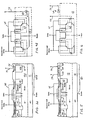
- the present invention provides a vertical DMOS power switching cell with an integral operating condition sensor, as cell 60a in cross-section Figure 3a. Further examples are shown as cells 60b, 60c, 60d and 80 in Figs. 3b, 3c, 3d and 5 Equivalent circuits are shown in schematic Figures 4a, 4b, 4c, 4d, and 6, respectively, with some regions corresponding to regions of Figure 1 DMOS cell 5 described above. Unlike prior art cell 5 with deep body region 23, this invention in Figure 3a cell 60a modifies deep body region 63a to have a greater lateral dimension, and to include additional and oppositely predoped or implanted well region 70.
- Well 70 serves as the cathode of diode 65 formed by the PN junction with body 63, which serves as the anode.
- conductivity types of all regions are reversed to provide a body region cathode and a well region anode.
- drain region 52, body region 62, and source region 34 form intrinsic NPN transistor 28, Figure 4a.
- well 70 added to body region 63a and substrate 52 forms intrinsic NPN transistor 66, Figure 4a.
- lead 75 does not forward bias transistor 66 base-emitter junction 65, transistor 66 is off and does not interfere with the normal switching operation of cell 60a.
- positively biased region 52 can provide a collector current to turn on transistor 66, adding lead 40 current to the lead 64a current measured across junction 65 and out lead 75.
- the intrinsic NPN transistor 66 current gain should be sufficiently low so that the collector 52 to emitter 70 with base 63a open breakdown voltage (BVceo) is not significantly lower, and encountered earlier, than its collector 52 to base 63a with emitter 70 breakdown voltage with the emitter shorted to the base (BVces).
- One way of obtaining low gain is to control doping so that base region 63a has a relatively high P-type dopant concentration compared to adjacent emitter junction 65 to obtain a low emitter injection efficiency, and to control doping so that base region 63a has a high net P-type dopant concentration per unit surface area of the base between base-emitter junction 65 and base-collector junction 61 to obtain a low base transport factor.
- cells 60b and 60c have sensor anode body regions 63b and 63c which are electrically isolated from P+ body regions 63, as shown in the corresponding schematic diagram Figures 4b and 4c.
- P+ body region 63b is electrically connected through overlying interconnect lead 36b, for example aluminum metallization, to body region 63.
- use of base-emitter junction 65 to measure the temperature within cell 60a or 60b requires only one additional cathode contact 75.
- Figure 3c cell 60c provides a second additional lead 64c to body region 63c, so that both sides of diode 65c are accessible, and test current does not have to use lead 64, which may be subject to transient effects during switching.
- This configuration allows a variety of electrical connections for sensing temperature.
- cell 60d in Figures 3d and 4d provides isolated P+ region 63d without an N+ well.
- P+ region 63d forms the anode of diode 61d with N-cathode region 52d.
- the absence of an intrinsic NPN transistor 66 mitigates the problem of reduced breakdown voltage.
- Cell 60d allows sensor diode 61d to be electrically referenced to drain region 52d.
- Figures 5 and 6 show another example in which cell 80 diode 68, formed in polycrystalline silicon or single crystal silicon recrystallized from poly silicon, is electrically isolated by dielectric 69, for example SiO2, from surface 53.
- Sensor diode 68 may be referenced to any external circuit voltage through anode lead 78 and cathode lead 79.
- Sensor diodes according to the present invention are formed similarly in combination DMOS-bipolar (insulated gate bipolar) transistor (IGBT) devices which correspond to DMOS transistors with the addition of a fourth region beneath, and of opposite conductivity type from, an epitaxial layer serving as region 52, as shown for example in U.S. Patent No. 4,443,931.
- IGBT insulated gate bipolar transistor
- substrate 50 comprises a second conductivity type wafer 51 for an IGBT anode, and a first conductivity type epitaxial layer 52 for the DMOS drain region.
- the present invention is compatible for use with a current mirror configuration to measure current as described above with reference to Figure 2, if it is desired to measure current separately from measuring temperature.
Landscapes
- Metal-Oxide And Bipolar Metal-Oxide Semiconductor Integrated Circuits (AREA)
- Insulated Gate Type Field-Effect Transistor (AREA)
- Micro-Organisms Or Cultivation Processes Thereof (AREA)
- Medicines Containing Material From Animals Or Micro-Organisms (AREA)
Description
- This invention relates to semiconductor devices and more specifically to a vertical double diffused metal oxide semiconductor (DMOS) power switching transistor device with an operating condition sensor.
- Prior art vertical DMOS transistor devices, as described for example in U.S. Patents No. 4,430,792 and 4,443,931 (which corresponds to EP-A-0 097 866) and reproduced in Figure 1, are field effect transistor (FET) cell structures in which a common substrate drain 10 serves multiple vertical DMOS cells. In
DMOS cell 5 on the right side ofdrain lead 40 and ofgate lead 25 in Figure 1, substrate drain 10 is formed from N+ wafer 11 with N-epitaxial layer 12, which sustains a high breakdown voltage. Beneathsubstrate surface 13, Ptype body diffusion 22 contains smaller, N+type source diffusion 34. Onsurface 13 overdrain 12 andadjacent body diffusion 22, gate dielectric 26 supportspolycrystalline silicon gate 24. In N-channel DMOS cell 5, a positive bias applied togate 24 establisheschannel 31 across the top ofbody 22 for electron flow fromsource 34 to drain 12. - In a typical power switching DMOS device as shown in Figure 1, a symmetrical pair of DMOS cells on the right and left share
common gate electrode 24, which enables current to flow simultaneously fromsources respective channels common drain 12.Body regions source region - So that
N+ source 34, P-body 22, and N-substrate 12 will not operate as anintrinsic NPN transistor 28, Figure 2,junctions surface 13 by common source/body contact(s) 36 to the adjacent P-body regions deep body regions forestall junctions - Rapid switching with a large substrate drain make DMOS devices well suited for high current density power switching applications, but high power switching dissipates large amounts of heat, which if not controlled can potentially destroy DMOS power switching devices. Therefore these devices need to be protected from overheating in some applications. Prior art DMOS devices have been protected from overheating by for example heat sink casings and/or external current limiting circuits. A thermal sensor can be positioned nearby and used in a feedback loop to control current, and thus temperature, in a DMOS device. However, these prior art methods may not indicate temperature precisely in
channel 22 andupper drain 12, or the amperage flowing throughcell 5, Figure 1. Large area devices such as high current DMOS transistors or other MOS gated devices can have sharp temperature gradients, making it important to sample temperatures near high current density regions. - One DMOS cell temperature measuring technique uses one of the cell's PN junctions for a test current, which is a function of junction bias and temperature. Such a junction test current is a more direct and accurate measurement of temperature than a normal operating cell channel current measurement, which also depends upon source-to-gate bias. To measure the
operating cell 5 current betweenleads junction 17, independently of achannel 31 current,gate 24 must be grounded and the lead 36-to-lead 40 bias must be reversed, interrupting normal operation ofcell 5. In many applications, continuous operation and/or external circuit requirements prohibit interrupting DMOS transistor operation for such measurements. - A prior art technique reported in Electronic Design, June 28, 1984, pp. 50-52, monitors operating DMOS device condition with a current mirror circuit, not shown. Current through a first transistor (e.g. the left side of Figure 2) is mirrored by proportional current through a second (mirror) transistor (e.g. the right side of Figure 2). The mirrored current can be measured through a resistor, not shown, in series with
lead 36, to indicate temperature without interrupting operation of the first transistor. - It is also known to provide diodes on a substrate for temperature sensing, as seen in German Application 2351732 and Japanese Application 54-54644; however, these diodes require a significant amount of silicon surface area and may be too distant from the device being measured to accurately measure the temperature of the device.
- There remains, therefore, a need for a DMOSFET power switching device in which temperature can be measured directly, accurately, and without interfering with device operation.
- Accordingly, the present invention provides a vertical DMOS cell structure having the features of claim 1.
- The present invention provides a DMOS power switching cell structure with an integral temperature sensor for accurately measuring temperature in the immediate vicinity of high density current, without interfering with normal power switching operation of the cell.
- While avoiding interference with operation, the invention makes an accurate temperature measurement by measuring a test current through, or a test voltage across a PN junction, provided by at least one new region of conductivity type opposite to the surrounding region of the cell, with a new electrical contact to the at least one region, and optionally a second electrical contact to the second region surrounding the first region.
- A first embodiment provides a DMOS cell with a new diode well in an extended deep body region, and provides an electrical contact to the new diode well.
- In the Accompanying Drawings :-
- Figure 1 is a cross section of a prior art vertical DMOS transistor including two cells;
- Figure 2 is a schematic of the structure of Figure 1;
- Figure 3a is a cross section of a vertical DMOS transistor device having an integral temperature sensing diode according to the present invention;
- Figs. 3 b,c,d are further examples of DMOS transistor devices with an integrated sensor diode
- Figures 4a, 4b, 4c, and 4d are schematics of the respective Figure 3 structures;
- Figure 5 is a cross section of another example which forms a temperature sensing diode from single crystal or polycrystalline silicon which is electrically isolated from the DMOS device; and
- Figure 6 is a schematic of the structure of Figure 5.
- The present invention provides a vertical DMOS power switching cell with an integral operating condition sensor, as
cell 60a in cross-section Figure 3a. Further examples are shown ascells DMOS cell 5 described above. Unlikeprior art cell 5 withdeep body region 23, this invention in Figure 3acell 60a modifiesdeep body region 63a to have a greater lateral dimension, and to include additional and oppositely predoped or implantedwell region 70. Well 70 serves as the cathode ofdiode 65 formed by the PN junction withbody 63, which serves as the anode. In other embodiments, not shown, conductivity types of all regions are reversed to provide a body region cathode and a well region anode. - As explained with reference to Figures 1 and 2 prior
art DMOS cell 5, in Figure3a cell 60a,drain region 52,body region 62, andsource region 34 formintrinsic NPN transistor 28, Figure 4a. Similarly, well 70 added tobody region 63a andsubstrate 52 forms intrinsic NPN transistor 66, Figure 4a. Whenlead 75 does not forward bias transistor 66 base-emitter junction 65, transistor 66 is off and does not interfere with the normal switching operation ofcell 60a. However, whenlead 75 is biased negatively with respect to channel/body lead 64a, to cause a test current acrossjunction 65, then during normal operation ofcell 60a, positivelybiased region 52 can provide a collector current to turn on transistor 66, addinglead 40 current to thelead 64a current measured acrossjunction 65 and outlead 75. To minimize this addition of current fromlead 40, the intrinsic NPN transistor 66 current gain should be sufficiently low so that thecollector 52 to emitter 70 withbase 63a open breakdown voltage (BVceo) is not significantly lower, and encountered earlier, than itscollector 52 tobase 63a withemitter 70 breakdown voltage with the emitter shorted to the base (BVces). One way of obtaining low gain is to control doping so thatbase region 63a has a relatively high P-type dopant concentration compared toadjacent emitter junction 65 to obtain a low emitter injection efficiency, and to control doping so thatbase region 63a has a high net P-type dopant concentration per unit surface area of the base between base-emitter junction 65 and base-collector junction 61 to obtain a low base transport factor. - In the examples of Figure 3b and 3c, cells 60b and 60c have sensor
anode body regions 63b and 63c which are electrically isolated fromP+ body regions 63, as shown in the corresponding schematic diagram Figures 4b and 4c. In Figure 3b, P+ body region 63b is electrically connected through overlying interconnect lead 36b, for example aluminum metallization, tobody region 63. In Figure 3a or 3b, use of base-emitter junction 65 to measure the temperature withincell 60a or 60b requires only oneadditional cathode contact 75. Alternatively, Figure 3c cell 60c provides a secondadditional lead 64c tobody region 63c, so that both sides of diode 65c are accessible, and test current does not have to uselead 64, which may be subject to transient effects during switching. This configuration allows a variety of electrical connections for sensing temperature. - The example as
cell 60d in Figures 3d and 4d providesisolated P+ region 63d without an N+ well.P+ region 63d forms the anode ofdiode 61d with N-cathode region 52d. The absence of an intrinsic NPN transistor 66 mitigates the problem of reduced breakdown voltage. Cell 60d allowssensor diode 61d to be electrically referenced to drainregion 52d. - Figures 5 and 6 show another example in which
cell 80 diode 68, formed in polycrystalline silicon or single crystal silicon recrystallized from poly silicon, is electrically isolated by dielectric 69, for example SiO₂, fromsurface 53. Sensor diode 68 may be referenced to any external circuit voltage throughanode lead 78 andcathode lead 79. - Sensor diodes according to the present invention are formed similarly in combination DMOS-bipolar (insulated gate bipolar) transistor (IGBT) devices which correspond to DMOS transistors with the addition of a fourth region beneath, and of opposite conductivity type from, an epitaxial layer serving as
region 52, as shown for example in U.S. Patent No. 4,443,931. In an IGBT, substrate 50 comprises a secondconductivity type wafer 51 for an IGBT anode, and a first conductivity typeepitaxial layer 52 for the DMOS drain region. - The present invention is compatible for use with a current mirror configuration to measure current as described above with reference to Figure 2, if it is desired to measure current separately from measuring temperature.
Claims (2)
- A vertical DMOS cell structure (60a) having a first conductivity type substrate drain (52), and beneath the upper surface of the substrate at least one second conductivity type body region (62), and within the body region (62) a first conductivity type source region (34), said cell structure (60a) being characterised by an operating condition sensor region (70) comprising a first region (70) of said first conductivity type in said body region (62), a first terminal (75) of said first region (70) for being connected so as to conduct a test current through or a test voltage across said first region (70) and said body region (62) while the cell is operating ordinarily.
- The structure as claimed in claim 1, wherein the first region (70) is formed in a laterally enlarged body region (62).
Applications Claiming Priority (2)
| Application Number | Priority Date | Filing Date | Title |
|---|---|---|---|
| US92996186A | 1986-11-12 | 1986-11-12 | |
| US929961 | 1986-11-12 |
Publications (3)
| Publication Number | Publication Date |
|---|---|
| EP0267447A2 EP0267447A2 (en) | 1988-05-18 |
| EP0267447A3 EP0267447A3 (en) | 1990-04-25 |
| EP0267447B1 true EP0267447B1 (en) | 1993-03-24 |
Family
ID=25458747
Family Applications (1)
| Application Number | Title | Priority Date | Filing Date |
|---|---|---|---|
| EP87114899A Expired - Lifetime EP0267447B1 (en) | 1986-11-12 | 1987-10-13 | A vertical dmos power transistor with an integral operating condition sensor |
Country Status (3)
| Country | Link |
|---|---|
| EP (1) | EP0267447B1 (en) |
| JP (1) | JP2552880B2 (en) |
| DE (1) | DE3784997T2 (en) |
Families Citing this family (8)
| Publication number | Priority date | Publication date | Assignee | Title |
|---|---|---|---|---|
| JP2698645B2 (en) * | 1988-05-25 | 1998-01-19 | 株式会社東芝 | MOSFET |
| US4980740A (en) * | 1989-03-27 | 1990-12-25 | General Electric Company | MOS-pilot structure for an insulated gate transistor |
| GB9206058D0 (en) * | 1992-03-20 | 1992-05-06 | Philips Electronics Uk Ltd | A semiconductor switch and a temperature sensing circuit for such a switch |
| GB9207849D0 (en) * | 1992-04-09 | 1992-05-27 | Philips Electronics Uk Ltd | A semiconductor device |
| DE4244272A1 (en) * | 1992-12-28 | 1994-06-30 | Daimler Benz Ag | Field effect controlled semiconductor device |
| US8310006B2 (en) * | 2009-09-21 | 2012-11-13 | Maxpower Semiconductor, Inc. | Devices, structures, and methods using self-aligned resistive source extensions |
| CN102684485B (en) * | 2011-03-09 | 2015-01-21 | 无锡维赛半导体有限公司 | Vertical complementary field effect tube |
| JP7033049B2 (en) * | 2018-11-16 | 2022-03-09 | 株式会社 日立パワーデバイス | Semiconductor devices and power conversion devices using them |
Family Cites Families (7)
| Publication number | Priority date | Publication date | Assignee | Title |
|---|---|---|---|---|
| JPS5240017B2 (en) * | 1972-10-16 | 1977-10-08 | ||
| JPS54112179A (en) * | 1978-02-23 | 1979-09-01 | Sony Corp | Semiconductor device |
| JPS57139963A (en) * | 1981-02-24 | 1982-08-30 | Matsushita Electronics Corp | Semiconductor device |
| JPS57173767A (en) * | 1981-04-20 | 1982-10-26 | Sony Corp | Heat resistance measurement for mos-fet element |
| JPS5884461A (en) * | 1981-11-13 | 1983-05-20 | Hitachi Ltd | Insulating gate type semiconductor device |
| US4443931A (en) * | 1982-06-28 | 1984-04-24 | General Electric Company | Method of fabricating a semiconductor device with a base region having a deep portion |
| DE3322669C2 (en) * | 1982-07-08 | 1986-04-24 | General Electric Co., Schenectady, N.Y. | A method of manufacturing a semiconductor device having insulated gate electrodes |
-
1987
- 1987-09-10 JP JP62227534A patent/JP2552880B2/en not_active Expired - Lifetime
- 1987-10-13 DE DE8787114899T patent/DE3784997T2/en not_active Expired - Lifetime
- 1987-10-13 EP EP87114899A patent/EP0267447B1/en not_active Expired - Lifetime
Also Published As
| Publication number | Publication date |
|---|---|
| DE3784997D1 (en) | 1993-04-29 |
| EP0267447A3 (en) | 1990-04-25 |
| JPS63129671A (en) | 1988-06-02 |
| DE3784997T2 (en) | 1993-07-22 |
| JP2552880B2 (en) | 1996-11-13 |
| EP0267447A2 (en) | 1988-05-18 |
Similar Documents
| Publication | Publication Date | Title |
|---|---|---|
| US4896196A (en) | Vertical DMOS power transistor with an integral operating condition sensor | |
| US10121866B2 (en) | Semiconductor device | |
| US6180966B1 (en) | Trench gate type semiconductor device with current sensing cell | |
| US4589004A (en) | Semiconductor device monolithically comprising a V-MOSFET and bipolar transistor isolated from each other | |
| US6144085A (en) | Power transistor device having hot-location and cool-location temperature sensors | |
| US5063307A (en) | Insulated gate transistor devices with temperature and current sensor | |
| US7385250B2 (en) | Semiconductor device | |
| US20220416064A1 (en) | Semiconductor device | |
| KR20000015138A (en) | Insulated gate bipolar transistor having a trench gate structure | |
| US5032880A (en) | Semiconductor device having an interposing layer between an electrode and a connection electrode | |
| JP3338185B2 (en) | Semiconductor device | |
| EP0494597B1 (en) | Trench-gate power semiconductor device | |
| JP7691809B2 (en) | Semiconductor device and method for manufacturing the same | |
| US20220352360A1 (en) | Semiconductor device | |
| US6060744A (en) | Semiconductor device with a main current cell region and a current detecting cell region | |
| US20230143787A1 (en) | Semiconductor device and manufacturing method of semiconductor device | |
| CN112543993B (en) | Semiconductor devices | |
| US5559355A (en) | Vertical MOS semiconductor device | |
| US6906399B2 (en) | Integrated circuit including semiconductor power device and electrically isolated thermal sensor | |
| CN116013901A (en) | Semiconductor device with sensing element | |
| EP0267447A2 (en) | A vertical DMOS power transistor with an integral operating condition sensor | |
| JP3489404B2 (en) | Insulated gate semiconductor device | |
| US5757034A (en) | Emitter switched thyristor | |
| JP7693809B2 (en) | Semiconductor devices and related methods for improved measurement - Patents.com | |
| EP0115098B1 (en) | Lateral dmos transistor device having an injector region |
Legal Events
| Date | Code | Title | Description |
|---|---|---|---|
| PUAI | Public reference made under article 153(3) epc to a published international application that has entered the european phase |
Free format text: ORIGINAL CODE: 0009012 |
|
| AK | Designated contracting states |
Kind code of ref document: A2 Designated state(s): BE DE FR GB IT NL |
|
| PUAL | Search report despatched |
Free format text: ORIGINAL CODE: 0009013 |
|
| AK | Designated contracting states |
Kind code of ref document: A3 Designated state(s): BE DE FR GB IT NL |
|
| 17P | Request for examination filed |
Effective date: 19900919 |
|
| 17Q | First examination report despatched |
Effective date: 19910826 |
|
| GRAA | (expected) grant |
Free format text: ORIGINAL CODE: 0009210 |
|
| AK | Designated contracting states |
Kind code of ref document: B1 Designated state(s): BE DE FR GB IT NL |
|
| PG25 | Lapsed in a contracting state [announced via postgrant information from national office to epo] |
Ref country code: FR Effective date: 19930324 Ref country code: BE Effective date: 19930324 |
|
| ITF | It: translation for a ep patent filed | ||
| REF | Corresponds to: |
Ref document number: 3784997 Country of ref document: DE Date of ref document: 19930429 |
|
| EN | Fr: translation not filed | ||
| PLBE | No opposition filed within time limit |
Free format text: ORIGINAL CODE: 0009261 |
|
| STAA | Information on the status of an ep patent application or granted ep patent |
Free format text: STATUS: NO OPPOSITION FILED WITHIN TIME LIMIT |
|
| 26N | No opposition filed | ||
| REG | Reference to a national code |
Ref country code: GB Ref legal event code: IF02 |
|
| PGFP | Annual fee paid to national office [announced via postgrant information from national office to epo] |
Ref country code: NL Payment date: 20030919 Year of fee payment: 17 |
|
| PGFP | Annual fee paid to national office [announced via postgrant information from national office to epo] |
Ref country code: GB Payment date: 20031008 Year of fee payment: 17 |
|
| PG25 | Lapsed in a contracting state [announced via postgrant information from national office to epo] |
Ref country code: GB Free format text: LAPSE BECAUSE OF NON-PAYMENT OF DUE FEES Effective date: 20041013 |
|
| PG25 | Lapsed in a contracting state [announced via postgrant information from national office to epo] |
Ref country code: NL Free format text: LAPSE BECAUSE OF NON-PAYMENT OF DUE FEES Effective date: 20050501 |
|
| GBPC | Gb: european patent ceased through non-payment of renewal fee |
Effective date: 20041013 |
|
| NLV4 | Nl: lapsed or anulled due to non-payment of the annual fee |
Effective date: 20050501 |
|
| PG25 | Lapsed in a contracting state [announced via postgrant information from national office to epo] |
Ref country code: IT Free format text: LAPSE BECAUSE OF NON-PAYMENT OF DUE FEES;WARNING: LAPSES OF ITALIAN PATENTS WITH EFFECTIVE DATE BEFORE 2007 MAY HAVE OCCURRED AT ANY TIME BEFORE 2007. THE CORRECT EFFECTIVE DATE MAY BE DIFFERENT FROM THE ONE RECORDED. Effective date: 20051013 |
|
| PGFP | Annual fee paid to national office [announced via postgrant information from national office to epo] |
Ref country code: DE Payment date: 20061130 Year of fee payment: 20 |