EP0265769A1 - Method and apparatus for measuring with an optical cutting beam - Google Patents
Method and apparatus for measuring with an optical cutting beam Download PDFInfo
- Publication number
- EP0265769A1 EP0265769A1 EP87114946A EP87114946A EP0265769A1 EP 0265769 A1 EP0265769 A1 EP 0265769A1 EP 87114946 A EP87114946 A EP 87114946A EP 87114946 A EP87114946 A EP 87114946A EP 0265769 A1 EP0265769 A1 EP 0265769A1
- Authority
- EP
- European Patent Office
- Prior art keywords
- image
- optical cutting
- cutting beam
- irradiated
- optical
- Prior art date
- Legal status (The legal status is an assumption and is not a legal conclusion. Google has not performed a legal analysis and makes no representation as to the accuracy of the status listed.)
- Granted
Links
Images


Classifications
-
- G—PHYSICS
- G01—MEASURING; TESTING
- G01B—MEASURING LENGTH, THICKNESS OR SIMILAR LINEAR DIMENSIONS; MEASURING ANGLES; MEASURING AREAS; MEASURING IRREGULARITIES OF SURFACES OR CONTOURS
- G01B11/00—Measuring arrangements characterised by the use of optical techniques
- G01B11/24—Measuring arrangements characterised by the use of optical techniques for measuring contours or curvatures
- G01B11/25—Measuring arrangements characterised by the use of optical techniques for measuring contours or curvatures by projecting a pattern, e.g. one or more lines, moiré fringes on the object
-
- G—PHYSICS
- G06—COMPUTING; CALCULATING OR COUNTING
- G06T—IMAGE DATA PROCESSING OR GENERATION, IN GENERAL
- G06T7/00—Image analysis
- G06T7/50—Depth or shape recovery
- G06T7/521—Depth or shape recovery from laser ranging, e.g. using interferometry; from the projection of structured light
Definitions
- the present invention relates generally to a method and an apparatus for measuring the shape of an object by using an optical cutting process for a visual recognition device or the like, or more in particular to a method and an apparatus for measurement with an optical cutting beam suitable for use in an environment subject to variations in external light or in the case where the reflection characteristics on the object are irregular.
- the original image of an object is picked up and stored in an image memory or the like.
- a slit light beam is projected on the object, and the original image is subtracted from the image thus obtained thereby to produce a differential image.
- This subtraction between images offsets the parts other than the slit light beam (optical cutting beam). That is to say, any part in the background which may be bright has no effect.
- small noises that are caused in parts other than the slit beam when the differential image is produced can be removed by an appropriate threshold process.
- the position of the optical cutting beam is determined by thinning or statistical means.
- the brightness change of the optical cutting beam assumes a symmetric form, thereby facilitating the determination of a central value.
- the light reflection characteristics of the surface of the object are irregular such as in the case where white numerals exist on the object surface and are covered by the optical cutting beam, however, the brightness of the optical cutting beam undergoes a variation. If a central value is determined from this brightness variation, the resulting figure would be deflected toward a higher reflection factor, thereby causing a problematic deterioration of the measurement accuracy.
- the object of the present invention is to provide a method and an apparatus for measurement with an optical cutting beam which are difficult to be affected by changes in external light or by the irregu larities of the reflection characteristics on the surface of an object.
- an apparatus for measuring an optical cutting beam comprising an optical system for irradiating a light flux parallel to the slit beam projected with the optical cutting beam on an object, in which an original image obtained when the parallel light is not projected is compared with an image obtained when the parallel illumination light is projected thereby to produce data on the reflection characteristics of the object, so that the image formed by irradiation of the optical cutting beam is corrected by data representing reflection characteristics.
- an image of the existing reflection characteristics is standardized on the basis of the brightness of the optical cutting beam, and this data is used to correct the differential image formed by subtraction between the image formed by irradiation of the optical cutting beam and the original image. In this manner, the reflection irregularities are removed and the measurement accuracy improved.
- FIG. 1 A configuration of an optical cutting beam measuring apparatus according to an embodiment of the present invention is shown in Fig. 1.
- reference numeral 1 designates a TV camera
- numeral 2 a slit beam projector for projecting an optical cutting beam on an object
- numeral 3 a parallel beam illumination device for projecting a light flux having substantially the same diameter as tubular enclosure
- numeral 4 a half mirror adapted to irradiate the object 6 with the light beam from the parallel light beam illumination unit 3 in the same direction as the slit beam.
- Numeral 5 designates an image processing unit for analyzing the image produced from the TV camera. The unit 5 also controls the slit beam projector 2 and the projector for the parallel beam illumination unit 3.
- an original image such as shown in Fig. 2a is picked up by the TV camera.
- the parallel beam illumination unit 3 is then lit and the image involved (Fig. 2b) is picked up by the TV camera 1.
- a differential image therebetween In view of the intensity of the lights irradiated between the original image and the parallel beam image, a differential image therebetween, if obtained, has a brightness data proportional to the light reflection characteristics of the object as shown in Fig. 3a.
- the slit beam projector 2 is then lit (with the parallel beam illumination unit 3 turned off) to produce an image shown in Fig. 2c.
- the original image of Fig. 2a is subtracted from the image of Fig. 2c thereby to produce a differential image shown in Fig. 3b.
- the irregularities of the reflection characteristics on the object surface causes a distortion of the brightness distribution of the slit beam. This distortion is removed by use of the differential image of Fig. 3a containing the reflection characteristics data of the object surface.
- a command is sent from the CPU 15 to an illumination I/O 13 to light the parallel light 3, so that an image under irradiation of parallel beams is picked up by the camera 1, and an image signal digitized by the A/D converter 7 is introduced into the image memory 8.
- a command is applied from the CPU 15 to the illumination I/O 13 to turn off the parallel light 3, and the image after the turning off (original image) is formed by the camera 1, so that an image signal digitized by the A/D converter 7 is obtained.
- the parallel-light-irradiated image stored in the image memory 8 is read out, and the differential between the two images is taken by the differential processor 9 thereby to produce an image data (hereinafter called "the reflection factor map data") containing the brightness data proportional to the light reflection characteristics shown in Fig. 3a.
- the reflection factor map data an image data containing the brightness data proportional to the light reflection characteristics shown in Fig. 3a.
- a command is sent from the CPU 15 to a data selector 10 in such a manner that the image data sent from the differential processor 9 is applied to the image memory 11 with the reflection factor data stored in the image memory 11.
- a command is then sent from the CPU 15 to the illumination I/O 13 to light the slit beam projector 2, and a slit beam irradiated image is formed by the camera 1, so that an image signal digitized by the A/D converter 7 is introduced into the image memory 8.
- a command is sent from the CPU 15 to the illumination I/O 13 thereby to turn off the slit beam light 2, and the image after the turning off (original image) is picked up by the camera 1, with the result that an image signal digitized by the A/D converter 7 is acquired, thus applying data to the differential processor 9.
- the slit beam irradiated image stored in the image memory 8 is read out, and the difference between the two images is determined by the differential processor 9, so that a differential image shown in Fig. 3b is obtained.
- the data selector 10 is thus controlled by the CPU 15 and the output data stored in the image memory 12.
- the reflection factor map data stored in the image memory is read by the CPU 15, and the reflection factor normalized data R(I, J) computed as above is stored in the memory 11.
- the computation of equation (1) is processed in the CPU 15, and the corrected data B(I, J0) is written in the image memory 11, 12 or a work memory 14.
- the resulting data is used to effect optical extraction in the manner specified in JP-A-59-197810 and the result is written in the work memory 14.
- a threshold value TH for removing noises is determined and used for computation of X(J) only when the brightness M(I) is higher tha e where there are a plurality of peaks exceeding TH, X(J) is computed where the area of a maximum is largest. The result of computation is written in the work memory 14.
Abstract
Description
- The present invention relates generally to a method and an apparatus for measuring the shape of an object by using an optical cutting process for a visual recognition device or the like, or more in particular to a method and an apparatus for measurement with an optical cutting beam suitable for use in an environment subject to variations in external light or in the case where the reflection characteristics on the object are irregular.
- In a conventional optical cutting beam measuring apparatus for a visual recognition system, as disclosed in JP-A-59-197810, subtraction is effected between an image irradiated with an optical cutting beam and an original image not so irradiated, and by thus removing the effect of the background light, the optical cutting beam is stably extracted.
- Specifically, according to the conventional optical cutting beam measurement method, first, the original image of an object is picked up and stored in an image memory or the like. Then, a slit light beam is projected on the object, and the original image is subtracted from the image thus obtained thereby to produce a differential image. This subtraction between images offsets the parts other than the slit light beam (optical cutting beam). That is to say, any part in the background which may be bright has no effect. In actual practice, small noises that are caused in parts other than the slit beam when the differential image is produced can be removed by an appropriate threshold process. After the optical cutting beam is separated from the background, the position of the optical cutting beam is determined by thinning or statistical means. In this method, as far as the radiation surface is uniform, the brightness change of the optical cutting beam assumes a symmetric form, thereby facilitating the determination of a central value. To the extent that the light reflection characteristics of the surface of the object are irregular such as in the case where white numerals exist on the object surface and are covered by the optical cutting beam, however, the brightness of the optical cutting beam undergoes a variation. If a central value is determined from this brightness variation, the resulting figure would be deflected toward a higher reflection factor, thereby causing a problematic deterioration of the measurement accuracy.
- The object of the present invention is to provide a method and an apparatus for measurement with an optical cutting beam which are difficult to be affected by changes in external light or by the irregu larities of the reflection characteristics on the surface of an object.
- In order to achieve the aforementioned object, there is provided according to the present invention an apparatus for measuring an optical cutting beam, comprising an optical system for irradiating a light flux parallel to the slit beam projected with the optical cutting beam on an object, in which an original image obtained when the parallel light is not projected is compared with an image obtained when the parallel illumination light is projected thereby to produce data on the reflection characteristics of the object, so that the image formed by irradiation of the optical cutting beam is corrected by data representing reflection characteristics. In this configuration, an image of the existing reflection characteristics is standardized on the basis of the brightness of the optical cutting beam, and this data is used to correct the differential image formed by subtraction between the image formed by irradiation of the optical cutting beam and the original image. In this manner, the reflection irregularities are removed and the measurement accuracy improved.
-
- Fig. 1 is a diagram show ing a configuration of an optical cutting beam measuring apparatus according to an embodiment of the present invention.
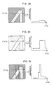
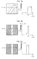
- Figs. 2a, 2b and 2c and Figs. 3a, 3b and 3c are diagrams for explaining the procedure for removing irradiation irregularities in an optical cutting beam measuring method according to the present invention.
- Fig. 4 is a flowchart showing the steps of the optical cutting beam measuring method according to the present invention.
- Fig. 5 is a diagram showing a configuration of an image processing unit for the optical cutting beam measuring apparatus according to the present invention.
- An embodiment of the present invention will be explained below with reference to Figs. 1 to 5.
- A configuration of an optical cutting beam measuring apparatus according to an embodiment of the present invention is shown in Fig. 1. In Fig. 1,
reference numeral 1 designates a TV camera, numeral 2 a slit beam projector for projecting an optical cutting beam on an object, numeral 3 a parallel beam illumination device for projecting a light flux having substantially the same diameter as tubular enclosure, and numeral 4 a half mirror adapted to irradiate the object 6 with the light beam from the parallel lightbeam illumination unit 3 in the same direction as the slit beam. Numeral 5 designates an image processing unit for analyzing the image produced from the TV camera. Theunit 5 also controls theslit beam projector 2 and the projector for the parallelbeam illumination unit 3. - A method of removing the effect of the reflection irregularities on the surface of the object will be explained with reference to Figs. 2a to 2c and Figs. 3a to 3c.
- First, an original image such as shown in Fig. 2a is picked up by the TV camera. The parallel
beam illumination unit 3 is then lit and the image involved (Fig. 2b) is picked up by theTV camera 1. In view of the intensity of the lights irradiated between the original image and the parallel beam image, a differential image therebetween, if obtained, has a brightness data proportional to the light reflection characteristics of the object as shown in Fig. 3a. - The
slit beam projector 2 is then lit (with the parallelbeam illumination unit 3 turned off) to produce an image shown in Fig. 2c. In order to remove the effect of the background light in the image, as in the method explained with reference to the prior art, the original image of Fig. 2a is subtracted from the image of Fig. 2c thereby to produce a differential image shown in Fig. 3b. - The graph of Fig. 3b shows a brightness distribution on the scanning line for the differential image J = J₀. The irregularities of the reflection characteristics on the object surface causes a distortion of the brightness distribution of the slit beam. This distortion is removed by use of the differential image of Fig. 3a containing the reflection characteristics data of the object surface.
- Now, explanation will be made of a method of removing a scanning line J = J₀ on the image. First, the I coordinate value I₀ of the brightest point on the differential image of the slit beam in Fig. 3b. Then, on the assumption that the brightness of I = I₀ on the same scanning line J = J₀ in Fig. 3a as 1 in value, other brightness values on the same scanning line J = J₀ are standardized. This standardized data is assumed to be
R(I, J n) (R(I₀, J₀) = 1)
and the brightness data of the slit beam differential image in Fig. 3b as
S(I, J₀)
the corrected data B(I, J₀) is determined as
B(I, J₀) = S(I, J₀)/R(I, J₀)
When corrected data on all the scanning lines are obtained by repeating this step, an image shown in Fig. 3c is acquired, thus correcting the reflection irregularities in the slit b eam. - Now, the operation of the
image processing unit 5 used for the aforementioned process will be explained with reference to Fig. 5. - First, a command is sent from the
CPU 15 to an illumination I/O 13 to light theparallel light 3, so that an image under irradiation of parallel beams is picked up by thecamera 1, and an image signal digitized by the A/D converter 7 is introduced into theimage memory 8. A command is applied from theCPU 15 to the illumination I/O 13 to turn off theparallel light 3, and the image after the turning off (original image) is formed by thecamera 1, so that an image signal digitized by the A/D converter 7 is obtained. In the process, in synchronism with this operation, the parallel-light-irradiated image stored in theimage memory 8 is read out, and the differential between the two images is taken by the differential processor 9 thereby to produce an image data (hereinafter called "the reflection factor map data") containing the brightness data proportional to the light reflection characteristics shown in Fig. 3a. At the same time, a command is sent from theCPU 15 to a data selector 10 in such a manner that the image data sent from the differential processor 9 is applied to the image memory 11 with the reflection factor data stored in the image memory 11. - A command is then sent from the
CPU 15 to the illumination I/O 13 to light theslit beam projector 2, and a slit beam irradiated image is formed by thecamera 1, so that an image signal digitized by the A/D converter 7 is introduced into theimage memory 8. A command is sent from theCPU 15 to the illumination I/O 13 thereby to turn off theslit beam light 2, and the image after the turning off (original image) is picked up by thecamera 1, with the result that an image signal digitized by the A/D converter 7 is acquired, thus applying data to the differential processor 9. In synchronism with this process, the slit beam irradiated image stored in theimage memory 8 is read out, and the difference between the two images is determined by the differential processor 9, so that a differential image shown in Fig. 3b is obtained. The data selector 10 is thus controlled by theCPU 15 and the output data stored in theimage memory 12. - The reflection factor map data stored in the image memory is read by the
CPU 15, and the reflection factor normalized data R(I, J) computed as above is stored in the memory 11. In this process, the brightness level is not necessarily in the range from 0 to 1, but may be 0 to 100 or 0 to 255 in the case where an 8-bit parallel data memory is used, the only requirement being that when the corrected data B(I, J₀) is computed, the following equation is obtained:
B(I, J₀) = S(I, J₀)/(R(I, J₀)/MAX) ..... (1)
(J₀ = 0 to 239)
where MAX is a maximum value. By using the reflection factor normalized data stored in the memory 11 and the slit beam differential image stored in thememory 12, the computation of equation (1) is processed in theCPU 15, and the corrected data B(I, J₀) is written in theimage memory 11, 12 or awork memory 14. The resulting data is used to effect optical extraction in the manner specified in JP-A-59-197810 and the result is written in thework memory 14. - The manner in which this process is used for optical extraction process in such a manner as described in JP-A-61-95203 will be explained.
- In a screen of 256 × 240, for example, assume that the brightness of the I-th pixel (0 ≦αµρ¨ I ≦αµρ¨ 255) on the J-th line (0 ≦αµρ¨ J ≦αµρ¨ 239) is M(I). The position X(J) of the optical cutting beam is defined as follows:

work memory 14. - It will thus be understood from the foregoing description that according to the present invention a measurement error of an optical cutting beam caused by the reflection irregularities on the surface of an object as well as the effect of an external light is reduced, and therefore the technique under consideration is applied under a variety of environments without affecting the measurement accuracy.
Claims (3)
picking up a first image that is an image of an object not irradiated with any additional light;
picking up a second image that is an image of the object irradiated with a parallel beam;
determining a differential image between the first and second images and measuring light reflection irregularities on the surface of the object from the differential image; and
correcting the reflection irregularities caused at the time of irradiation of the optical cutting beam by means of the above-mentioned measurement.
a camera (1) for picking up an image of an object;
a slit beam projector (2) for irradiating the object with an optical cutting beam;
a parallel beam illumination system (3) for irradiating for irradiating the object from the same direction as the slit beam for optical cutting; and
an image processing unit (5) for measuring the light reflection irregularities on the surface of an object of measurement from the differential image between an image of the object irradiated with no additional light and an image of the object irradiated with a parallel beam, and correcting the reflection irregularities caused at the time of irradiation of the optical cutting beam by means of the measurement.
Applications Claiming Priority (2)
| Application Number | Priority Date | Filing Date | Title |
|---|---|---|---|
| JP245225/86 | 1986-10-17 | ||
| JP61245225A JPH0629707B2 (en) | 1986-10-17 | 1986-10-17 | Optical cutting line measuring device |
Publications (2)
| Publication Number | Publication Date |
|---|---|
| EP0265769A1 true EP0265769A1 (en) | 1988-05-04 |
| EP0265769B1 EP0265769B1 (en) | 1990-09-05 |
Family
ID=17130507
Family Applications (1)
| Application Number | Title | Priority Date | Filing Date |
|---|---|---|---|
| EP87114946A Expired - Lifetime EP0265769B1 (en) | 1986-10-17 | 1987-10-13 | Method and apparatus for measuring with an optical cutting beam |
Country Status (4)
| Country | Link |
|---|---|
| US (1) | US4779002A (en) |
| EP (1) | EP0265769B1 (en) |
| JP (1) | JPH0629707B2 (en) |
| DE (1) | DE3764766D1 (en) |
Cited By (7)
| Publication number | Priority date | Publication date | Assignee | Title |
|---|---|---|---|---|
| EP0399138A2 (en) * | 1989-02-28 | 1990-11-28 | Siemens Aktiengesellschaft | Method for three-dimensional examination of printed circuits |
| DE3940518A1 (en) * | 1989-12-07 | 1991-06-20 | Fisw Gmbh | Illumination control for optical distance meter - measures intensity distribution along section line, enables optimal illumination |
| DE4001298A1 (en) * | 1990-01-18 | 1991-07-25 | Nordischer Maschinenbau | METHOD FOR THREE-DIMENSIONAL LIGHT-OPTICAL MEASURING OF OBJECTS AND DEVICE FOR IMPLEMENTING THE METHOD |
| EP0448803A2 (en) * | 1990-03-28 | 1991-10-02 | GRUNDIG E.M.V. Elektro-Mechanische Versuchsanstalt Max Grundig holländ. Stiftung & Co. KG. | Video control system |
| FR2696542A1 (en) * | 1992-10-05 | 1994-04-08 | Controle Ind | Optical detector and test system for metrological use - has structured plane light source, diffused light source and a matrix camera in same enclosure |
| GB2311853A (en) * | 1996-04-05 | 1997-10-08 | Mitutoyo Corp | Optical gauge |
| TWI565928B (en) * | 2014-12-22 | 2017-01-11 | 財團法人工業技術研究院 | A differential triangular measurement system and method thereof |
Families Citing this family (3)
| Publication number | Priority date | Publication date | Assignee | Title |
|---|---|---|---|---|
| US6765224B1 (en) * | 2000-12-29 | 2004-07-20 | Cognex Corporation | Machine vision method and system for the inspection of a material |
| US6531707B1 (en) * | 2000-12-29 | 2003-03-11 | Cognex Corporation | Machine vision method for the inspection of a material for defects |
| CN109443199B (en) * | 2018-10-18 | 2019-10-22 | 天目爱视(北京)科技有限公司 | 3D information measuring system based on intelligent light source |
Citations (2)
| Publication number | Priority date | Publication date | Assignee | Title |
|---|---|---|---|---|
| US4498778A (en) * | 1981-03-30 | 1985-02-12 | Technical Arts Corporation | High speed scanning method and apparatus |
| US4594001A (en) * | 1981-07-07 | 1986-06-10 | Robotic Vision Systems, Inc. | Detection of three-dimensional information with a projected plane of light |
Family Cites Families (2)
| Publication number | Priority date | Publication date | Assignee | Title |
|---|---|---|---|---|
| JPS60200103A (en) * | 1984-03-26 | 1985-10-09 | Hitachi Ltd | Light cutting-plate line extraction circuit |
| US4645917A (en) * | 1985-05-31 | 1987-02-24 | General Electric Company | Swept aperture flying spot profiler |
-
1986
- 1986-10-17 JP JP61245225A patent/JPH0629707B2/en not_active Expired - Lifetime
-
1987
- 1987-10-13 EP EP87114946A patent/EP0265769B1/en not_active Expired - Lifetime
- 1987-10-13 DE DE8787114946T patent/DE3764766D1/en not_active Expired - Lifetime
- 1987-10-19 US US07/109,313 patent/US4779002A/en not_active Expired - Lifetime
Patent Citations (2)
| Publication number | Priority date | Publication date | Assignee | Title |
|---|---|---|---|---|
| US4498778A (en) * | 1981-03-30 | 1985-02-12 | Technical Arts Corporation | High speed scanning method and apparatus |
| US4594001A (en) * | 1981-07-07 | 1986-06-10 | Robotic Vision Systems, Inc. | Detection of three-dimensional information with a projected plane of light |
Non-Patent Citations (2)
| Title |
|---|
| PATENT ABSTRACTS OF JAPAN, Unexamined Applications, Field P, Vol. 9, No. 127, May 31, 1985 The Patent Office Japanese Government page 10 P 360 *Kokai-No. 60-10 105* * |
| PATENT ABSTRACTS OF JAPAN, Unexamined Applications, Field P, Vol. 9, No. 62, March 19, 1985 The Patent Office Japanese Government page 123 P 342 *Kokai-No. 59-197 810* & JP-A-59-197 810 (Ishikawajima) * |
Cited By (11)
| Publication number | Priority date | Publication date | Assignee | Title |
|---|---|---|---|---|
| EP0399138A2 (en) * | 1989-02-28 | 1990-11-28 | Siemens Aktiengesellschaft | Method for three-dimensional examination of printed circuits |
| EP0399138A3 (en) * | 1989-02-28 | 1992-03-04 | Siemens Aktiengesellschaft | Method for three-dimensional examination of printed circuits |
| DE3940518A1 (en) * | 1989-12-07 | 1991-06-20 | Fisw Gmbh | Illumination control for optical distance meter - measures intensity distribution along section line, enables optimal illumination |
| DE4001298A1 (en) * | 1990-01-18 | 1991-07-25 | Nordischer Maschinenbau | METHOD FOR THREE-DIMENSIONAL LIGHT-OPTICAL MEASURING OF OBJECTS AND DEVICE FOR IMPLEMENTING THE METHOD |
| EP0448803A2 (en) * | 1990-03-28 | 1991-10-02 | GRUNDIG E.M.V. Elektro-Mechanische Versuchsanstalt Max Grundig holländ. Stiftung & Co. KG. | Video control system |
| EP0448803A3 (en) * | 1990-03-28 | 1992-09-23 | Grundig E.M.V. Elektro-Mechanische Versuchsanstalt Max Grundig Hollaend. Stiftung & Co. Kg. | Video control system |
| FR2696542A1 (en) * | 1992-10-05 | 1994-04-08 | Controle Ind | Optical detector and test system for metrological use - has structured plane light source, diffused light source and a matrix camera in same enclosure |
| GB2311853A (en) * | 1996-04-05 | 1997-10-08 | Mitutoyo Corp | Optical gauge |
| US5856874A (en) * | 1996-04-05 | 1999-01-05 | Mitutoyo Corporation | Optical gauge with adjustable light path bending mirror |
| GB2311853B (en) * | 1996-04-05 | 2000-02-23 | Mitutoyo Corp | Optical gauge |
| TWI565928B (en) * | 2014-12-22 | 2017-01-11 | 財團法人工業技術研究院 | A differential triangular measurement system and method thereof |
Also Published As
| Publication number | Publication date |
|---|---|
| JPS63100304A (en) | 1988-05-02 |
| DE3764766D1 (en) | 1990-10-11 |
| JPH0629707B2 (en) | 1994-04-20 |
| US4779002A (en) | 1988-10-18 |
| EP0265769B1 (en) | 1990-09-05 |
Similar Documents
| Publication | Publication Date | Title |
|---|---|---|
| CA1252216A (en) | Apparatus for automatically inspecting objects and identifying or recognizing known and unknown portions thereof, including defects and the like and method | |
| US5097516A (en) | Technique for illuminating a surface with a gradient intensity line of light to achieve enhanced two-dimensional imaging | |
| US5566244A (en) | Method of inspecting a workpiece surface including a picturing system with a shortened focal plane | |
| US5379347A (en) | Method of inspecting the surface of a workpiece | |
| EP0265769B1 (en) | Method and apparatus for measuring with an optical cutting beam | |
| JPH07260701A (en) | Recognition method of area of inspection | |
| KR930002347B1 (en) | Pattern position recognition apparatus | |
| US5373567A (en) | Method and apparatus for pattern matching | |
| JPS62232504A (en) | Position detector | |
| US6597805B1 (en) | Visual inspection method for electronic device, visual inspecting apparatus for electronic device, and record medium for recording program which causes computer to perform visual inspecting method for electronic device | |
| US6888958B1 (en) | Method and apparatus for inspecting patterns | |
| JP3260425B2 (en) | Pattern edge line estimation method and pattern inspection device | |
| JPH05164703A (en) | Inspecting method for surface of workpiece | |
| JP3262150B2 (en) | Inspection device for solder joints | |
| JP3093450B2 (en) | Semiconductor chip recognition device | |
| JP3025562B2 (en) | Surface condition inspection method using bright and dark illumination | |
| JPS6326508A (en) | Inspection device for packaging component | |
| JPS6343037B2 (en) | ||
| JPH05164700A (en) | Method for inspecting work surface | |
| JP3517100B2 (en) | Pattern inspection apparatus and pattern inspection method | |
| JP2701872B2 (en) | Surface inspection system | |
| JP2919556B2 (en) | Image processing system | |
| JPH06174437A (en) | Bonding wire inspection device | |
| JPH05126545A (en) | Shape measuring instrument | |
| JPH05303662A (en) | Stereo character reading method using light-section method |
Legal Events
| Date | Code | Title | Description |
|---|---|---|---|
| PUAI | Public reference made under article 153(3) epc to a published international application that has entered the european phase |
Free format text: ORIGINAL CODE: 0009012 |
|
| AK | Designated contracting states |
Kind code of ref document: A1 Designated state(s): DE FR GB |
|
| 17P | Request for examination filed |
Effective date: 19880506 |
|
| 17Q | First examination report despatched |
Effective date: 19890706 |
|
| GRAA | (expected) grant |
Free format text: ORIGINAL CODE: 0009210 |
|
| AK | Designated contracting states |
Kind code of ref document: B1 Designated state(s): DE FR GB |
|
| REF | Corresponds to: |
Ref document number: 3764766 Country of ref document: DE Date of ref document: 19901011 |
|
| ET | Fr: translation filed | ||
| PLBE | No opposition filed within time limit |
Free format text: ORIGINAL CODE: 0009261 |
|
| STAA | Information on the status of an ep patent application or granted ep patent |
Free format text: STATUS: NO OPPOSITION FILED WITHIN TIME LIMIT |
|
| 26N | No opposition filed | ||
| PGFP | Annual fee paid to national office [announced via postgrant information from national office to epo] |
Ref country code: FR Payment date: 20010830 Year of fee payment: 15 |
|
| PGFP | Annual fee paid to national office [announced via postgrant information from national office to epo] |
Ref country code: GB Payment date: 20011003 Year of fee payment: 15 |
|
| PGFP | Annual fee paid to national office [announced via postgrant information from national office to epo] |
Ref country code: DE Payment date: 20011228 Year of fee payment: 15 |
|
| REG | Reference to a national code |
Ref country code: GB Ref legal event code: IF02 |
|
| PG25 | Lapsed in a contracting state [announced via postgrant information from national office to epo] |
Ref country code: GB Free format text: LAPSE BECAUSE OF NON-PAYMENT OF DUE FEES Effective date: 20021013 |
|
| PG25 | Lapsed in a contracting state [announced via postgrant information from national office to epo] |
Ref country code: DE Free format text: LAPSE BECAUSE OF NON-PAYMENT OF DUE FEES Effective date: 20030501 |
|
| GBPC | Gb: european patent ceased through non-payment of renewal fee |
Effective date: 20021013 |
|
| PG25 | Lapsed in a contracting state [announced via postgrant information from national office to epo] |
Ref country code: FR Free format text: LAPSE BECAUSE OF NON-PAYMENT OF DUE FEES Effective date: 20030630 |
|
| REG | Reference to a national code |
Ref country code: FR Ref legal event code: ST |