EP0265122B1 - Endanschlussmodul - Google Patents
Endanschlussmodul Download PDFInfo
- Publication number
- EP0265122B1 EP0265122B1 EP19870308903 EP87308903A EP0265122B1 EP 0265122 B1 EP0265122 B1 EP 0265122B1 EP 19870308903 EP19870308903 EP 19870308903 EP 87308903 A EP87308903 A EP 87308903A EP 0265122 B1 EP0265122 B1 EP 0265122B1
- Authority
- EP
- European Patent Office
- Prior art keywords
- module
- blades
- terminals
- printed circuit
- terminal
- Prior art date
- Legal status (The legal status is an assumption and is not a legal conclusion. Google has not performed a legal analysis and makes no representation as to the accuracy of the status listed.)
- Expired - Lifetime
Links
Images


Classifications
-
- H—ELECTRICITY
- H01—ELECTRIC ELEMENTS
- H01R—ELECTRICALLY-CONDUCTIVE CONNECTIONS; STRUCTURAL ASSOCIATIONS OF A PLURALITY OF MUTUALLY-INSULATED ELECTRICAL CONNECTING ELEMENTS; COUPLING DEVICES; CURRENT COLLECTORS
- H01R12/00—Structural associations of a plurality of mutually-insulated electrical connecting elements, specially adapted for printed circuits, e.g. printed circuit boards [PCB], flat or ribbon cables, or like generally planar structures, e.g. terminal strips, terminal blocks; Coupling devices specially adapted for printed circuits, flat or ribbon cables, or like generally planar structures; Terminals specially adapted for contact with, or insertion into, printed circuits, flat or ribbon cables, or like generally planar structures
- H01R12/50—Fixed connections
- H01R12/51—Fixed connections for rigid printed circuits or like structures
- H01R12/515—Terminal blocks providing connections to wires or cables
Definitions
- This invention is directed generally to terminal modules for housing small circuits which are electrically connected across field wiring terminals and, more particularly, to modularized packages which are adapted for concurrent physical and electrical connection to two or more terminals on a frame containing a plurality of field wiring terminals.
- a primary application of the invention is in electrical data acquisition systems using microprocessors and other monitoring circuitry mounted on printed circuit boards to manage data input and output, such as for providing control and protection functions for systems in electrical power plants and generators.
- a common prior practice in applications as referred to above is to physically terminate the wire leads of the electronic components directly to the screw terminals used for the field wiring.
- This arrangement not only gives the appearance of a last minute design change, but exposes the electronic component or components to physical damage during assembly, maintenance or other events.
- the performance and maintenance of the external components is sensitive to unforeseen installation mistakes, such as shorting of the component to the chassis where the proper assembly technique is not followed. Further, it is readily seen that where plural components are to be connected across two or more field terminals, the method of direct attachment of the components to the terminals becomes even less desirable.
- a typical prior art approach has been to contain an external component in a potted box or other potting means, with metal connector blades or pins extending out of the potting material. Basically this constitutes simply an encapsulation of the component in order to protect it, and does not provide the desired ability to achieve reliable electrical and mechanical attachment.
- a terminal module for attaching to a plurality of terminals, of a terminal assembly, in use, comprising a printed circuit board having a plurality of extending conductive blades for physical and electrical connection to respective ones of said terminals characterized by, a potted component enclosure housing at least a portion of said printed circuit board for enclosing an electronic component mounted on said printed circuit board, said conductive blades protruding from said potted component means, electrical conductor means on said printed circuit board for defining a plurality of circuit points of said electronic component means and for making electrical connections between respective ones of said circuit points and respective ones of said blades, whereby when said blades are connected to said terminals, said circuit points are in electrical connection with said terminals.
- a terminal module which is a compact assembly of predetermined geometry which is attached to two or more terminals of a terminal block connector.
- the module comprises a printed circuit board having a first portion which carries one or more circuit components and which is potted within a rectangular plastic shell. The remainder of the integral printed circuit board protrudes from the shell and has blade portions configured for use both as electrical terminals and for physical attachment to the screw terminals of the terminal connector.
- the module thus provides the advantages of a standardized package which is adapted to carry a plurality of components and for making reliable mechanical and electrical connection to the field terminals.
- the printed circuit board assembly as described herein can be used for reliable and efficient mounting of components, the module further providing efficient means for attaching the entire assembly to the field terminals.
- a flame-retardant potting shell is utilized along with an encapsulating material which reduces risk of flammability.
- a resilient high-temperature pre-coating is placed over the electronic components prior to the encapsulation to prevent breakage by stresses set up when the encapsulant is curing.
- the printed circuit is provided with plate-through holes and a double sided circuit pattern for connecting the components, thereby providing redundant paths on each side of the board and better connection at the terminal.
- the invention further employs necked-down etched circuitry to increase the creep distance between the board circuit conductors at the point of entry into the encapsulant.
- the shell housing the component assembly is preferably a rectangular shell which carries identifying markings and date codes. A polarity mark is etched into the board circuitry to verify correct assembly and installation of polarity sensitive circuitry on the screw terminals.
- the modular design of this invention provides for and embraces ready extension to applications requiring connection to more than two terminals and/or non-adjacent terminals.
- the use of the integral printed circuit board enables any desired combination of components to be reliably connected to a terminal block.
- the terminal module disclosed in this specification is used in conjunction with a terminal block connector which provides connections through to one or more printed circuit boards, such as is disclosed, for example, in U.S. Patent 4,542,443, Rinefierd, Jr., assigned to the same assignee.
- the Rinefierd patent discloses what is referred to therein as a termination frame assembly, and more particularly a stack of termination frame assemblies mounted in a cabinet.
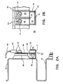
- Figure 1 represents substantially the same drawing as presented in Fig. 3 of U.S. Patent 4,542,443, and shows a termination frame assembly, referred to herein as a termination frame 40 having thereon two terminal strips 45, each strip 45 having a plurality of screw-type terminals 47 aligned in a horizontal array. As seen more particularly in Fig.
- a terminal module unit 50 is attached to a pair of adjacent terminals 47 of the strip 45. Although just one such terminal module 50 is illustrated as being so connected, it is to be understood that any appropriate number of such modules may be connected to terminals 47. Furthermore, it is within the scope of the invention that the modules be connected to two or more terminals 47, which terminals may be adjacent or non-adjacent depending upon the application involved. Reference may be made to the aforementioned U.S. Patent 4,542,443 for a discussion of the manner and means by which printed circuit boards, including microprocessors, are mounted to the other side of termination frame 40 and in electrical connection with terminals 47 for managing data input and output, and the manner by which wiring from field locations is connected through to the termination frame 40.
- a module 50 mounted in mechanical and electrical connection with a pair of adjacent terminals 47.
- a field wire 48 and wiring lug 49 are shown connected to a terminal 47.
- the module comprises a one-piece integral circuit board 51 which, as illustrated, has two upper portions or blades 58, 59 which are physically separated by a slot 60.
- the blades have holes 64 (see also Fig. 3A) in the upper portions thereof of a size and spacing to enable mounting of the module onto terminals 47 and mechanical connection thereto.
- the lower portion of the printed circuit board as seen in Fig. 2A, carries one or more electrical components electrically wired thereto and shown symbolically at 56.
- the lower portion carrying the component assembly is housed within a substantially rectangular plastic shell 52, the component assembly being contained within encapsulant 53. Although components are illustrated as being on only one side of the board 51, they may be contained on either or both sides.
- the potted assembly comprising elements 52, 53, 56 and the lower portion of the board 51 is referred to as the potted component means 54.
- the shell 52 is a flame retardant material such as diallyl phthalate
- the encapsulating material may be a two part epoxy comprising an epoxy casting resin and a catalyst.
- the resin is mixed in a container until uniform in texture, at which time 8-9% by weight of the catalyst is blended thoroughly therein.
- the mixture is then poured into the potting shell 52 to the indicated level.
- a resilient high temperature pre-coating of an RTV silicone is utilized for pre-coating the electronic components, so as to prevent breakage, e.g., of glass diode packages by stresses set up by the encapsulant when curing.
- a plurality of terminal strips 45 may be stacked one on top of another, leaving a gap therebetween.
- the terminal module is designed so that the shell 52 fits just below the forwardly extending portion of the terminal strip and between vertically aligned adjacent terminal strips.
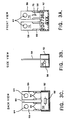
- the terminal module unit 50 is illustrated diagrammatically in front, side and rear views.
- Each of the blades 58, 59 of the block has a conductive surface which is preferably a copper coating covered with tin plating.
- This surface is neck-down etched as shown at 66 to increase the creep distance between the circuit conductors at the point of their entry into the encapsulant 53.
- the use of the printed circuit terminal conductor surfaces, or tabs avoids fractures usually associated with work-hardening of tabs comprised of all copper which may occur under continuous vibration conditions at the stress concentration point.
- the rectangular shell is adapted for carrying identifying markings and/or date codes, which provides an important advantage for field installations of this nature.
- a polarity mark is etched into the circuitry on one of the blades to verify the correct assembly and installation of polarity sensitive circuitry on the screw terminals.
- different colored potting shells are used for each unique function or component assembly, to make assembly inspection and maintenance for the system easier, simpler and more reliable.
- FIGs. 4A and 4B there are shown diagrammatic views of opposite sides of a printed circuit board carrying a component assembly comprising a capacitor C1 in parallel with a series combination of diodes D1, D2 and D3.
- each of the main terminal tabs, or conductive pathways 72, 73 is printed on each side of the respective blades 58, 59.
- the circuit conductive material on the printed circuit board is double-side-printed with plated-through holes 76 connecting the opposite sides.
- redundant paths are provided on each side of each blade, thereby providing improved reliability over the technique of depending merely on one soldered connection for each component lead.
- the double sided printed blade also insures excellent connection at the point of the electrical contact with the screw terminal 47.
- the single integral printed circuit board which performs the dual functions of carrying a circuit component assembly in predetermined wired form as well as, of providing reliable means for electrical and mechanical connection to the field terminals, provides distinct advantages over the prior art.
- the module provides simple but reliable packaging of components in standardized packages, thereby simplifying installation in the field.
Claims (9)
- Anschlußmodul (50) zum Befestigen einer Vielzahl von Anschlüssen (47) einer gebräuchlichen Anschlußzusammenstellung, das aufweist:
eine Leiterplatte (51) mit einer Vielzahl von sich erstreckenden leitenden Kontaktblättern (58) für physikalische und elektrische Verbindung zu jeweiligen Anschlüssen,
gekennzeichnet durch
eine vergossene Bauteilumhüllung (54), die zumindest einen Teil der Leiterplatte aufnimmt, zum Einschließen eines auf der Leiterplatte befestigten elektronischen Bauteils, wobei die leitenden Kontaktblätter aus dem vergossenen Bauteilmittel herausragen,
elektrische Leitermittel (78) auf der Leiterplatte zum Festlegen einer Vielzahl von Schaltungspunkten (76) des elektronischen Bauteilmittels und zum Herstellen von elektrischen Verbindungen zwischen jeweiligen Schaltungspunkten und jeweiligen Kontaktblättern (58), wodurch, wenn die Blätter mit den Anschlüssen verbunden sind, die Schaltungspunkte in elektrischer Verbindung mit den Anschlüssen sind. - Modul nach Anspruch 1, worin die Leiterplatte beidseitig Material der gedruckten Schaltung mit dort durchkontaktierten Löchern aufweist, wodurch redundante Leiterwege auf jeder Seite von jedem Blatt bereitgestellt werden.
- Modul nach Anspruch 1, worin die vergossene Bauteilumhüllung eine Vielzahl von elektrisch mit der Leiterplatte verbundenen Bauteilen aufweist.
- Modul nach Anspruch 3, worin die vergossene Bauteilumhüllung einen Gußmantel (52) zum Einschließen der Bauteile und ein Vergußmaterial innerhalb des Mantels zum Einschließen der Bauteile aufweist.
- Modul nach Anspruch 4, worin der Gußmantel aus einem abbrandverzögernden Material besteht und mit einem abbrandverzögernden Vergußmaterial gefüllt ist.
- Endanschlußmodul nach Anspruch 1, worin eine Polaritätsmarke in eines der Blätter geätzt ist, um den korrekten Zusammenbau und die Installation zu erleichtern.
- Modul nach Anspruch 1, worin jedes der Blätter eine vorgegebene ähnliche Geometrie aufweist, und die Blätter entsprechend einem notwendigen Anschlußabstand voneinander beabstandet sind.
- Modul nach Anspruch 7, worin die vergossene Bauteilumhüllung ein Gehäuse aufweist, das den unteren Teil der Leiterplatte an beiden Seiten umschließt, und worin die Blätter sich vom Gehäuse aus erstrecken.
- Modul nach Anspruch 8, worin die Blätter geätzten Leiterschaltungsaufbau auf jeder ihrer Seiten aufweisen, wobei der Schaltungsaufbau am Eintrittspunkt in das vergossene Bauteilmittel abwärts verjüngt ist, um dadurch die Kriechstrecke zwischen den Blattleiteroberflächen zu vergrößern.
Applications Claiming Priority (2)
| Application Number | Priority Date | Filing Date | Title |
|---|---|---|---|
| US91485586A | 1986-10-03 | 1986-10-03 | |
| US914855 | 1986-10-03 |
Publications (3)
| Publication Number | Publication Date |
|---|---|
| EP0265122A2 EP0265122A2 (de) | 1988-04-27 |
| EP0265122A3 EP0265122A3 (en) | 1989-10-18 |
| EP0265122B1 true EP0265122B1 (de) | 1993-06-23 |
Family
ID=25434866
Family Applications (1)
| Application Number | Title | Priority Date | Filing Date |
|---|---|---|---|
| EP19870308903 Expired - Lifetime EP0265122B1 (de) | 1986-10-03 | 1987-10-02 | Endanschlussmodul |
Country Status (2)
| Country | Link |
|---|---|
| EP (1) | EP0265122B1 (de) |
| JP (1) | JPS6391974A (de) |
Family Cites Families (5)
| Publication number | Priority date | Publication date | Assignee | Title |
|---|---|---|---|---|
| GB1303849A (de) * | 1970-10-29 | 1973-01-24 | ||
| JPS5937970U (ja) * | 1982-09-02 | 1984-03-10 | 本田技研工業株式会社 | 自動二輪車の熱交換器 |
| US4542443A (en) * | 1983-08-08 | 1985-09-17 | Westinghouse Electric Corp. | Termination frame assembly with protection from EMI from field wiring and rack for same |
| US4591950A (en) * | 1983-09-09 | 1986-05-27 | American Manufacturing Company, Inc. | Circuit board-terminal-housing assembly |
| DE3439410A1 (de) * | 1984-10-27 | 1986-04-30 | Stribel GmbH, 7443 Frickenhausen | Einrichtung fuer ein kraftfahrzeug |
-
1987
- 1987-10-02 JP JP62248184A patent/JPS6391974A/ja active Granted
- 1987-10-02 EP EP19870308903 patent/EP0265122B1/de not_active Expired - Lifetime
Also Published As
| Publication number | Publication date |
|---|---|
| EP0265122A3 (en) | 1989-10-18 |
| JPH0451951B2 (de) | 1992-08-20 |
| JPS6391974A (ja) | 1988-04-22 |
| EP0265122A2 (de) | 1988-04-27 |
Similar Documents
| Publication | Publication Date | Title |
|---|---|---|
| EP0746967B1 (de) | Elektronischer einsatz fuer ein elektronisches system und dessen herstellungsverfahren | |
| US5249979A (en) | Self-mounting bus | |
| US6609914B2 (en) | High speed and density circular connector for board-to-board interconnection systems | |
| US6342998B1 (en) | Data surge protection module | |
| US4603377A (en) | Main distributing frame board for an electronic switching system | |
| EP0000630B1 (de) | Fassung zur Verbindung von Mikroschaltkreisen | |
| GB2027289A (en) | Apparatus for effecting electrical connections to modular hardware | |
| EP0960468A1 (de) | Mehrstöckiges stromwandlermodul | |
| EP0916171A1 (de) | Verbinder mit schaltungsanordnung und anzeigen | |
| US5671121A (en) | Kangaroo multi-package interconnection concept | |
| CA2431623A1 (en) | Inner component board assembly for an electric utility meter | |
| US4792880A (en) | Terminal module | |
| US3939444A (en) | Printed circuit mountable, self grounding, multiple filter module | |
| EP0265122B1 (de) | Endanschlussmodul | |
| EP0643448B1 (de) | Koaxialverbinder zur Verbindung mit Leiterplatten | |
| US5616034A (en) | Power supply apparatus for package | |
| US5446621A (en) | Platform module system for a larger electronic system | |
| US3522486A (en) | Control apparatus | |
| JPS62181610A (ja) | 電子回路内蔵ジヨイントボツクス | |
| US3139560A (en) | Circuit board assembly | |
| US20030211759A1 (en) | Adapter for surface mount devices to through hole applications | |
| US4389697A (en) | Circuit assembly having a component with leads extending therefrom and a connector both supported on a planar substrate | |
| CA1207047A (en) | Electrically connecting | |
| EP0516455B1 (de) | Elektrische, eigensichere Schnittstelleneinrichtungen | |
| US20240014678A1 (en) | Battery Management System |
Legal Events
| Date | Code | Title | Description |
|---|---|---|---|
| PUAI | Public reference made under article 153(3) epc to a published international application that has entered the european phase |
Free format text: ORIGINAL CODE: 0009012 |
|
| AK | Designated contracting states |
Kind code of ref document: A2 Designated state(s): BE CH FR GB IT LI SE |
|
| PUAL | Search report despatched |
Free format text: ORIGINAL CODE: 0009013 |
|
| AK | Designated contracting states |
Kind code of ref document: A3 Designated state(s): BE CH FR GB IT LI SE |
|
| RHK1 | Main classification (correction) |
Ipc: H05K 5/00 |
|
| 17P | Request for examination filed |
Effective date: 19900215 |
|
| 17Q | First examination report despatched |
Effective date: 19920625 |
|
| ITF | It: translation for a ep patent filed |
Owner name: ING. ZINI MARANESI & C. S.R.L. |
|
| GRAA | (expected) grant |
Free format text: ORIGINAL CODE: 0009210 |
|
| AK | Designated contracting states |
Kind code of ref document: B1 Designated state(s): BE CH FR GB IT LI SE |
|
| PGFP | Annual fee paid to national office [announced via postgrant information from national office to epo] |
Ref country code: FR Payment date: 19930630 Year of fee payment: 7 |
|
| ET | Fr: translation filed | ||
| PGFP | Annual fee paid to national office [announced via postgrant information from national office to epo] |
Ref country code: CH Payment date: 19930831 Year of fee payment: 7 |
|
| PGFP | Annual fee paid to national office [announced via postgrant information from national office to epo] |
Ref country code: GB Payment date: 19930928 Year of fee payment: 7 |
|
| PGFP | Annual fee paid to national office [announced via postgrant information from national office to epo] |
Ref country code: BE Payment date: 19931018 Year of fee payment: 7 |
|
| PGFP | Annual fee paid to national office [announced via postgrant information from national office to epo] |
Ref country code: SE Payment date: 19931029 Year of fee payment: 7 |
|
| PLBE | No opposition filed within time limit |
Free format text: ORIGINAL CODE: 0009261 |
|
| STAA | Information on the status of an ep patent application or granted ep patent |
Free format text: STATUS: NO OPPOSITION FILED WITHIN TIME LIMIT |
|
| 26N | No opposition filed | ||
| PG25 | Lapsed in a contracting state [announced via postgrant information from national office to epo] |
Ref country code: GB Effective date: 19941002 |
|
| PG25 | Lapsed in a contracting state [announced via postgrant information from national office to epo] |
Ref country code: SE Effective date: 19941003 |
|
| PG25 | Lapsed in a contracting state [announced via postgrant information from national office to epo] |
Ref country code: LI Effective date: 19941031 Ref country code: CH Effective date: 19941031 Ref country code: BE Effective date: 19941031 |
|
| EAL | Se: european patent in force in sweden |
Ref document number: 87308903.1 |
|
| BERE | Be: lapsed |
Owner name: WESTINGHOUSE ELECTRIC CORP. Effective date: 19941031 |
|
| GBPC | Gb: european patent ceased through non-payment of renewal fee |
Effective date: 19941002 |
|
| PG25 | Lapsed in a contracting state [announced via postgrant information from national office to epo] |
Ref country code: FR Effective date: 19950630 |
|
| REG | Reference to a national code |
Ref country code: CH Ref legal event code: PL |
|
| EUG | Se: european patent has lapsed |
Ref document number: 87308903.1 |
|
| REG | Reference to a national code |
Ref country code: FR Ref legal event code: ST |
|
| PG25 | Lapsed in a contracting state [announced via postgrant information from national office to epo] |
Ref country code: IT Free format text: LAPSE BECAUSE OF NON-PAYMENT OF DUE FEES;WARNING: LAPSES OF ITALIAN PATENTS WITH EFFECTIVE DATE BEFORE 2007 MAY HAVE OCCURRED AT ANY TIME BEFORE 2007. THE CORRECT EFFECTIVE DATE MAY BE DIFFERENT FROM THE ONE RECORDED. Effective date: 20051002 |