EP0264644A2 - Circuit arrangement for simulating the NSI contact by means of the hold circuit in a two-way telephone set - Google Patents
Circuit arrangement for simulating the NSI contact by means of the hold circuit in a two-way telephone set Download PDFInfo
- Publication number
- EP0264644A2 EP0264644A2 EP87113787A EP87113787A EP0264644A2 EP 0264644 A2 EP0264644 A2 EP 0264644A2 EP 87113787 A EP87113787 A EP 87113787A EP 87113787 A EP87113787 A EP 87113787A EP 0264644 A2 EP0264644 A2 EP 0264644A2
- Authority
- EP
- European Patent Office
- Prior art keywords
- circuit
- subscriber line
- arrangement
- hold circuit
- switched
- Prior art date
- Legal status (The legal status is an assumption and is not a legal conclusion. Google has not performed a legal analysis and makes no representation as to the accuracy of the status listed.)
- Withdrawn
Links
Images
Classifications
-
- H—ELECTRICITY
- H04—ELECTRIC COMMUNICATION TECHNIQUE
- H04M—TELEPHONIC COMMUNICATION
- H04M3/00—Automatic or semi-automatic exchanges
- H04M3/42—Systems providing special services or facilities to subscribers
- H04M3/58—Arrangements for transferring received calls from one subscriber to another; Arrangements affording interim conversations between either the calling or the called party and a third party
-
- H—ELECTRICITY
- H04—ELECTRIC COMMUNICATION TECHNIQUE
- H04M—TELEPHONIC COMMUNICATION
- H04M1/00—Substation equipment, e.g. for use by subscribers
- H04M1/26—Devices for calling a subscriber
- H04M1/30—Devices which can set up and transmit only one digit at a time
- H04M1/31—Devices which can set up and transmit only one digit at a time by interrupting current to generate trains of pulses; by periodically opening and closing contacts to generate trains of pulses
- H04M1/312—Devices which can set up and transmit only one digit at a time by interrupting current to generate trains of pulses; by periodically opening and closing contacts to generate trains of pulses pulses produced by electronic circuits
-
- H—ELECTRICITY
- H04—ELECTRIC COMMUNICATION TECHNIQUE
- H04M—TELEPHONIC COMMUNICATION
- H04M9/00—Arrangements for interconnection not involving centralised switching
- H04M9/002—Arrangements for interconnection not involving centralised switching with subscriber controlled access to a line, i.e. key telephone systems
Definitions
- the invention relates to a circuit arrangement for emulating the NSI contact by means of the electronic hold circuit in a two-way telephone with microprocessor control fed via the subscriber line, with a rectifier bridge per subscriber line as reverse polarity protection, with a keypad for subscriber selection and for special functions, with a speech circuit with a switching device for Choice of the subscriber line to be occupied and with an electronic hold circuit between the wires of each subscriber line, the hold circuit containing a current path which can be switched on and off via the microprocessor and consists of the series connection of a thyristor, a load resistor and a series transistor.
- the above-mentioned telephone stations are known as two-way telephones (two-way telephones, operating instructions of the Germanierepost FeTAp 2L-716-796), whereby the individual subscriber lines can be optionally switched on, for example, with the aid of lockable buttons, and the necessary between the a / b wires when asked or brokered Holding resistors can be switched on and off by contacts of the buttons or by relay contacts.
- the object of the invention is now to expand the electronic hold circuit without much effort so that it can also be used as an NSI contact during the dialing process at the telephone station, the circuit arrangement should be integrable, the voltage (high voltage) separation of the subscriber line and speech circuit and a control with controls designed only for low currents.
- the circuit arrangement is explained using a drawing.
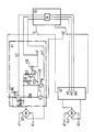
- the drawing shows a speech circuit SS with a Microprocessor M, the two holding circuits H1 and H2, the rectifier bridges Gl1 and Gl2 intended as reverse polarity protection, the two subscriber lines a1 / b1 and a2 / b2 and the two line changeover contacts l1 and l2.
- the two holding circuits H1 and H2 are of the same type.
- the holding circuit H1 shows further details such as the thyristor Ty with the holding circuit C / R1, the holding resistor or load resistor RL, the series transistor T1, the transistor optocouplers T2 and T5 and the switching transistors T3 and T4.
- the control connection points for the microprocessor are given as m1, m2 and m3 (m4, m5 and m6 for H2).
- the optically controlled thyristor Ty receives an ignition pulse via the control terminal m1, whereby it switches through and remains switched through by a holding current determined via C and R1.
- the current path for the direct current applied via the rectifier bridge Gl1 runs through the thyristor Ty, the load resistor RL and the series transistor T1. The latter is switched on because part of the holding current is tapped from Ty and acts as the base current of T1, which in turn the holding current for Ty is maintained.
- the latter goes into the blocking circuit and thus also interrupts the holding current for the thyristor Ty, which now also interrupts the current path.
- the load resistor RL from the subscriber line a1 / b1 is thus switched.
- the potential at m3 can also be switched off.
- the holding circuit H2 with the control points m4, m5 and m6 works accordingly. If this hold circuit, for example H1, is to function as an NSI contact, then it must cut or short-circuit the wires a1 / b1 of the subscriber line in time with the dialing pulses.
- a pulse is given via the control point m1 to the optically controlled transistor Ty, so that, as already described, this switches through, forms its holding current and the base current for the series transistor T1, the latter also switching through.
- the current path is now switched through.
- the load resistor RL is now bridged via the diodes D1 and D2 and the transistors T3 and T4 (arrangement of semiconductor components) since there is no potential at the control point M3.
- the transistor optocoupler thus remains in the blocking state and the holding current can result from the resistor R2 or the current through the current path form a base voltage which switches on the transistors T3 and T4.
- the two diodes D1 and D2 serve to drop a defined voltage across the resistor R2.
- the opening of the NSI contact corresponding to the selection clock is effected in that a control pulse is applied to the control point m2, whereby the transistor optocoupler switches through, which in turn derives the base current of the series transistor T1.
- the series transistor turns off. The current path is thus interrupted and the thyristor T4 is switched into the blocking state.
- the hold circuit H2 functions analogously when a subscriber is selected via the subscriber line a2 / b2.
- the voltage + UB in the figure is the respective operating voltage of the semiconductor elements Ty, T2 and T3.
Abstract
Description
Die Erfindung betrifft eine Schaltungsanordnung zur Nachbildung des NSI-Kontaktes mittels der elektronischen Halteschaltung in einem über die Teilnehmerleitung gespeisten Zweiwegefernsprecher mit Mikroprozessorsteuerung, mit einer Gleichrichterbrücke je Teilnehmerleitung als Verpolungsschutz, mit einem Tastenblock für die Teilnehmerwahl und für Sonderfunktionen, mit einer Sprechschaltung mit einer Umschalteinrichtung zur Wahl der zu belegenden Teilnehmerleitung und mit je einer elektronischen Halteschaltung zwischen den Adern jeder Teilnehmerleitung, wobei die Halteschaltung einen über den Mikroprozessor an- und abschaltbaren, aus der Serienschaltung eines Thyristors, eines Lastwiderstandes und eines Längstransistors bestehenden Strompfad enthält.The invention relates to a circuit arrangement for emulating the NSI contact by means of the electronic hold circuit in a two-way telephone with microprocessor control fed via the subscriber line, with a rectifier bridge per subscriber line as reverse polarity protection, with a keypad for subscriber selection and for special functions, with a speech circuit with a switching device for Choice of the subscriber line to be occupied and with an electronic hold circuit between the wires of each subscriber line, the hold circuit containing a current path which can be switched on and off via the microprocessor and consists of the series connection of a thyristor, a load resistor and a series transistor.
Obengenannte Fernsprechstationen sind als Zweiwegefernsprecher bekannt (Zweiwegefernsprecher, Bedienungsanleitung der Deutschen Bundespost FeTAp 2L-716-796), wobei die einzelnen Teilnehmerleitungen beispielsweise mit Hilfe verrastbarer Tasten wahlweise angeschaltet werden können und wobei bei Rückfrage oder beim Makeln die zwischen den a/b-Adern notwendigen Haltewiderstände durch Kontakte der Tasten oder durch Relaiskontakte an- und abgeschaltet werden können.The above-mentioned telephone stations are known as two-way telephones (two-way telephones, operating instructions of the German Bundespost FeTAp 2L-716-796), whereby the individual subscriber lines can be optionally switched on, for example, with the aid of lockable buttons, and the necessary between the a / b wires when asked or brokered Holding resistors can be switched on and off by contacts of the buttons or by relay contacts.
Um Relais und konstruktiv aufwendige verrastende Tasten zu vermeiden, ist bereits vorgeschlagen worden, die notwendige Halteschaltung elektronisch auszuführen, so daß sie mit Hilfe des in der Fernsprechstation enthaltenen Mikroprozessors über die Tastatur (Tastenblock) der Fernsprechstation gesteuert werden kann. Das bedeutet, daß eine Teilnehmerleitung im Wartezustand über einen einen Haltewiderstand aufweisenden Strompfad abgeschlossen ist und daß im nachfolgenden Betriebszustand (Gesprächszustand) dieser Teilnehmerleitung der Strompfad gesperrt wird.In order to avoid relays and structurally complex latching keys, it has already been proposed to carry out the necessary hold circuit electronically so that it can be operated with the aid of the microprocessor contained in the telephone station can be controlled via the keypad (keypad) of the telephone station. This means that a subscriber line in the waiting state is terminated via a current path having a holding resistor and that the current path is blocked in the subsequent operating state (call state) of this subscriber line.
Die Aufgabe der Erfindung soll nun darin bestehen, die elektronische Halteschaltung ohne großen Aufwand so auszubauen, daß sie zusätzlich als NSI-Kontakt beim Wählvorgang an der Fernsprechstation verwendet werden kann, wobei die Schaltungsanordnung integrierbar sein soll, wobei die spannungsmäßige (Hochspannung) Trennung von Teilnehmerleitung und Sprechschaltung und eine Steuerung mit nur für geringe Ströme ausgelegten Bedienungselementen gegeben ist.The object of the invention is now to expand the electronic hold circuit without much effort so that it can also be used as an NSI contact during the dialing process at the telephone station, the circuit arrangement should be integrable, the voltage (high voltage) separation of the subscriber line and speech circuit and a control with controls designed only for low currents.
Dies wird dadurch erreicht, daß zur Nachbildung des geschlossenen NSI-Kontaktes der Strompfad durchgeschaltet ist, wobei der darin enthaltene Lastwiderstand durch eine Anordnung von Halbleiterbausteinen überbrückt ist und wobei die Steuerung der Anordnung über einen seinerseits von dem Mikrocomputer gesteuerten Transistor-Optokoppler erfolgt und daß zur Nachbildung des geöffneten NSI-Kontaktes der Längstransistor und der Thyristor durch den Mikroprozessor im Sperrzustand gesteuert werden.This is achieved in that the current path is switched through to simulate the closed NSI contact, the load resistance contained therein being bridged by an arrangement of semiconductor components and the arrangement being controlled by a transistor optocoupler which is itself controlled by the microcomputer, and in that Replication of the open NSI contact of the series transistor and the thyristor can be controlled by the microprocessor in the blocking state.
Hieraus ergibt sich der Vorteil, daß der den geschlossenen NSI-Kontakt anzeigende Kurzschluß zwischen den a/b-Adern und die den offenen NSI-Kontakt darstellende vollständige Auftrennung der Halteschaltung gegeben ist, daß die Schaltungsanordnung integrierbar ist, die Steuerung mit leistungsschwachen Bedienelementen möglich ist und auch eine galvanische Trennung von Teilnehmerleitung und Sprechschaltung vorliegt.This has the advantage that the short circuit between the a / b wires, which indicates the closed NSI contact, and the complete separation of the holding circuit, which represents the open NSI contact, is given, that the circuit arrangement can be integrated, and control with low-performance control elements is possible and there is also a galvanic separation of the subscriber line and speech circuit.
Die Schaltungsanordnung wird anhand einer Zeichnung erklärt. Die Zeichnung zeigt eine Sprechschaltung SS mit einem Mikroprozessor M, die beiden Halteschaltungen H1 und H2, die als Verpolungsschutz gedachten Gleichrichterbrücken Gl1 und Gl2, die beiden Teilnehmerleitungen a1/b1 und a2/b2 und die beiden Leitungsumschaltkontakte l1 und l2.The circuit arrangement is explained using a drawing. The drawing shows a speech circuit SS with a Microprocessor M, the two holding circuits H1 and H2, the rectifier bridges Gl1 and Gl2 intended as reverse polarity protection, the two subscriber lines a1 / b1 and a2 / b2 and the two line changeover contacts l1 and l2.
Die beiden Halteschaltungen H1 und H2 sind von gleicher Bauart. Die Halteschaltung H1 zeigt nähere Einzelheiten wie den Thyristor Ty mit dem Haltekreis C/R1, dem Haltewiderstand oder Lastwiderstand RL, dem Längstransistor T1, den Transistor-Optokopplern T2 und T5 und den Schalttransistoren T3 und T4. Außerdem sind die Steueranschlußpunkte für den Mikroprozessor mit m1, m2 und m3 angegeben (m4, m5 und m6 für H2).The two holding circuits H1 and H2 are of the same type. The holding circuit H1 shows further details such as the thyristor Ty with the holding circuit C / R1, the holding resistor or load resistor RL, the series transistor T1, the transistor optocouplers T2 and T5 and the switching transistors T3 and T4. In addition, the control connection points for the microprocessor are given as m1, m2 and m3 (m4, m5 and m6 for H2).
Nachstehend wird die Funktion der Schaltungsanordnung näher erläutert.The function of the circuit arrangement is explained in more detail below.
Im Ruhezustand der Schaltungsanordnung z.B. für die Halteschaltung H1 liegt an den Steuerpunkten m1, m2 und m3 kein Potential an. Es sei nun angenommen, daß zuerst über die Teilnehmerleitung a1/b1 gewählt und gesprochen wurde, daß dann durch Betätigen einer hierfür gewählten Taste des Tastenblocks eine Umschaltung z.B. zwecks Rückfrage auf die Teilnehmerleitung a2/b2 eingeleitet wurde, wobei auf Grund der gewählten Taste auch angesagt wurde, daß die Teilnehmerleitung a1/b1 in Wartestellung zu halten sei. Der Mikroprozessor M erkennt den Teilnehmerwunsch. Er schaltet in nicht dargestellter Weise die Umschaltkontakte l1 und l2 in der in der Figur gezeigten Weise. Der optisch gesteuerte Thyristor Ty erhält einen Zündimpuls über den Steueranschluß m1, wodurch er durchschaltet und durch einen über C und R1 bestimmten Haltestrom durchgeschaltet bleibt. Der Strompfad für den über die Gleichrichterbrücke Gl1 anliegenden Gleichstrom verläuft über den Thyristor Ty, den Lastwiderstand RL und den Längstransistor T1. Letzterer ist leitend geschaltet, denn es wird ein Teil des Haltestromes von Ty abgezweigt und wirkt als Basisstrom von T1, wodurch wiederum der Haltestrom für Ty aufrechterhalten wird.In the idle state of the circuit arrangement, for example for the holding circuit H1, there is no potential at the control points m1, m2 and m3. It is now assumed that dialing via the subscriber line a1 / b1 was first carried out, and then that a switch was initiated by pressing a key of the keypad selected for this purpose, for example for inquiring about the subscriber line a2 / b2, with the announcement due to the selected key was that the subscriber line a1 / b1 should be kept on hold. The microprocessor M recognizes the participant's request. It switches the changeover contacts l1 and l2 in a manner not shown in the manner shown in the figure. The optically controlled thyristor Ty receives an ignition pulse via the control terminal m1, whereby it switches through and remains switched through by a holding current determined via C and R1. The current path for the direct current applied via the rectifier bridge Gl1 runs through the thyristor Ty, the load resistor RL and the series transistor T1. The latter is switched on because part of the holding current is tapped from Ty and acts as the base current of T1, which in turn the holding current for Ty is maintained.
Gleichzeitig liegt ein Dauerpotential am Steuerpunkt m3 an, wodurch der Transistor-Optokoppler T5 durchgeschaltet wird. Dieses Durchschalten bedeutet, daß sich für die Basis des Transistors T4 über den Widerstand R2 keine Basisspannung aufbauen kann, so daß sich die Transistoren T3 und T4 im Sperrzustand befinden. Damit ist der Lastwiderstand RL nicht überbrückt und kann bei dem vorstehenden Betriebszustand als Haltewiderstand wirksam werden. Soll die Teilnehmerleitung a1/b1 jetzt wieder durch eine Tastenbetätigung am Tastenblock auf Gesprächsbetrieb (zum wartenden Teilnehmer) geschaltet werden, dann erfolgt über den Steuerpunkt m2 ein Impuls auf den Transistor-Optokoppler T2. Dieser wird durchgeschaltet und schaltet dadurch den Basisstrom für den Längstransistor T1 ab. Letzterer geht in Sperrschaltung und unterbricht damit auch den Haltestrom für den Thyristor Ty, der nun auch den Strompfad unterbricht. Somit ist der Lastwiderstand RL aus der Teilnehmerleitung a1/b1 geschaltet. Das Potential an m3 kann ebenfalls abgeschaltet werden. Die Halteschaltung H2 mit den Steuerpunkten m4, m5 und m6 arbeitet entsprechend.
Wenn diese Halteschaltung -z.B. H1- als NSI-Kontakt funktionieren soll, dann muß sie im Takt der Wählimpulse die Adern a1/b1 der Teilnehmerleitung auftrennen bzw. kurzschließen.At the same time there is a permanent potential at the control point m3, whereby the transistor optocoupler T5 is switched through. This switching means that no base voltage can build up for the base of the transistor T4 via the resistor R2, so that the transistors T3 and T4 are in the blocking state. The load resistor RL is thus not bridged and can act as a holding resistor in the above operating state. If the subscriber line a1 / b1 is now to be switched back to talk mode (to the waiting subscriber) by pressing a button on the keypad, then a pulse is sent to the transistor optocoupler T2 via the control point m2. This is switched through and thereby switches off the base current for the series transistor T1. The latter goes into the blocking circuit and thus also interrupts the holding current for the thyristor Ty, which now also interrupts the current path. The load resistor RL from the subscriber line a1 / b1 is thus switched. The potential at m3 can also be switched off. The holding circuit H2 with the control points m4, m5 and m6 works accordingly.
If this hold circuit, for example H1, is to function as an NSI contact, then it must cut or short-circuit the wires a1 / b1 of the subscriber line in time with the dialing pulses.
Zum Kurzschließen der Adern a1/b1 wird ein Impuls über den Steuerpunkt m1 auf den optisch gesteuerten Transistor Ty gegeben, so daß dieser, wie bereits geschildert, durchschaltet, seinen Haltestrom und den Basisstrom für den Längstransistor T1 bildet, wobei letzterer ebenfalls durchschaltet. Der Strompfad ist damit durchgeschaltet. Der Lastwiderstand RL ist jetzt über die Dioden D1 und D2 und die Transistoren T3 und T4 (Anordnung von Halbleiterbausteinen) überbrückt, da am Steuerpunkt M3 kein Potential anliegt. Somit bleibt der Transistor-Optokoppler im Sperrzustand und über den Widerstand R2 kann sich aus dem Haltestrom bzw. dem Strom durch den Strompfad eine Basisspannung ausbilden, die die Transistoren T3 und T4 durchschaltet. Die beiden Dioden D1 und D2 dienen dazu, um an dem Widerstand R2 eine definierte Spannung abfallen zu lassen.To short-circuit the wires a1 / b1, a pulse is given via the control point m1 to the optically controlled transistor Ty, so that, as already described, this switches through, forms its holding current and the base current for the series transistor T1, the latter also switching through. The current path is now switched through. The load resistor RL is now bridged via the diodes D1 and D2 and the transistors T3 and T4 (arrangement of semiconductor components) since there is no potential at the control point M3. The transistor optocoupler thus remains in the blocking state and the holding current can result from the resistor R2 or the current through the current path form a base voltage which switches on the transistors T3 and T4. The two diodes D1 and D2 serve to drop a defined voltage across the resistor R2.
Das dem Wähltakt entsprechende Öffnen des NSI-Kontaktes erfolgt dadurch, daß ein Steuerimpuls auf den Steuerpunkt m2 gegeben wird, wodurch der Transistor-Optokoppler durchschaltet, wodurch wiederum der Basisstrom des Längstransistors T1 abgeleitet wird. Der Längstransistor geht in Sperrzustand. Damit wird der Strompfad unterbrochen und der Thyristor T4 in Sperrzustand geschaltet.The opening of the NSI contact corresponding to the selection clock is effected in that a control pulse is applied to the control point m2, whereby the transistor optocoupler switches through, which in turn derives the base current of the series transistor T1. The series transistor turns off. The current path is thus interrupted and the thyristor T4 is switched into the blocking state.
Analog funktioniert die Halteschaltung H2 bei einer Teilnehmerwahl über die Teilnehmerleitung a2/b2. Die Spannung +UB in der Figur ist die jeweilige Betriebsspannung der Halbleiterelemente Ty, T2 und T3. Aus dem Obenstehenden geht hervor, daß nach der erfindungsgemäßen Schaltungsanordnung die elektronische Halteschaltung für Zweiwegefernsprecher in einfacher Weise als NSI-Kontakt mitverwendet werden kann. Der hier nicht behandelte NSA-Kontakt kann beispielsweise durch ein Schaltelement des vorzugsweise elektronischen Gabelumschalters realisiert werden.The hold circuit H2 functions analogously when a subscriber is selected via the subscriber line a2 / b2. The voltage + UB in the figure is the respective operating voltage of the semiconductor elements Ty, T2 and T3. From the above it can be seen that, according to the circuit arrangement according to the invention, the electronic hold circuit for two-way telephones can be used in a simple manner as an NSI contact. The NSA contact not dealt with here can be implemented, for example, by a switching element of the preferably electronic fork switch.
Claims (1)
dadurch gekennzeichnet,
daß zur Nachbildung des geschlossenen NSI-Kontaktes der Strompfad (Ty, RL, T1) durchgeschaltet ist, wobei der darin enthaltene Lastwiderstand (RL) durch eine Anordnung von Halbleiterbausteinen (T3, T4) überbrückt ist und wobei die Steuerung der Anordnung über einen seinerseits von dem Mikrocomputer (M) gesteuerten Transistor-Optokoppler (T5) erfolgt und daß zur Nachbildung des geöffneten NSI-Kontaktes der Längstransistor (T1) und der Thyristor (Ty) durch den Mikroprozessor (M) in Sperrzustand gesteuert werden.Circuit arrangement for simulating the NSI contact by means of the electronic hold circuit in a two-way telephone with microprocessor control fed via the subscriber line, with a rectifier bridge for each subscriber line as protection against polarity reversal, with a keypad for subscriber selection and for special functions, with a speech circuit with a switchover device for selecting the one to be used Subscriber line and each with an electronic hold circuit between the wires of each subscriber line, the hold circuit containing a current path which can be switched on and off via the microprocessor and consists of the series connection of a thyristor, a load resistor and a series transistor,
characterized,
that to simulate the closed NSI contact, the current path (Ty, RL, T1) is switched through, the load resistor (RL) contained therein being bridged by an arrangement of semiconductor components (T3, T4) and the control of the arrangement in turn by one of the microcomputer (M) controlled transistor optocoupler (T5) and that to simulate the open NSI contact, the series transistor (T1) and the thyristor (Ty) are controlled by the microprocessor (M) in the off state.
Applications Claiming Priority (2)
| Application Number | Priority Date | Filing Date | Title |
|---|---|---|---|
| DE3632200 | 1986-09-23 | ||
| DE3632200 | 1986-09-23 |
Publications (2)
| Publication Number | Publication Date |
|---|---|
| EP0264644A2 true EP0264644A2 (en) | 1988-04-27 |
| EP0264644A3 EP0264644A3 (en) | 1989-06-14 |
Family
ID=6310099
Family Applications (1)
| Application Number | Title | Priority Date | Filing Date |
|---|---|---|---|
| EP87113787A Withdrawn EP0264644A3 (en) | 1986-09-23 | 1987-09-21 | Circuit arrangement for simulating the nsi contact by means of the hold circuit in a two-way telephone set |
Country Status (4)
| Country | Link |
|---|---|
| EP (1) | EP0264644A3 (en) |
| AU (1) | AU600523B2 (en) |
| FI (1) | FI874140A (en) |
| IN (1) | IN167984B (en) |
Cited By (1)
| Publication number | Priority date | Publication date | Assignee | Title |
|---|---|---|---|---|
| ES2046112A2 (en) * | 1992-04-24 | 1994-01-16 | Revenga Ingenieros S A | Telephone equipment for direct point to point lines |
Families Citing this family (1)
| Publication number | Priority date | Publication date | Assignee | Title |
|---|---|---|---|---|
| IN164858B (en) * | 1986-09-11 | 1989-06-17 | Siemens Ag |
Citations (3)
| Publication number | Priority date | Publication date | Assignee | Title |
|---|---|---|---|---|
| DE3131299A1 (en) * | 1981-08-07 | 1983-03-17 | Siemens AG, 1000 Berlin und 8000 München | Circuit arrangement for telephone switching systems, in particular small PABX system, for which external connections can be set up to exchanges requiring loop dialling or DTMF dialling |
| US4490583A (en) * | 1983-02-14 | 1984-12-25 | Circom, Inc. | Plural line telephone controller |
| JPS6152053A (en) * | 1984-08-20 | 1986-03-14 | Nec Corp | Dial impulse transmission circuit |
Family Cites Families (2)
| Publication number | Priority date | Publication date | Assignee | Title |
|---|---|---|---|---|
| NL7907134A (en) * | 1979-09-25 | 1981-03-27 | Ericsson Telefon Mij | TELEPHONE INSTALLATION OF THE TYPE INDICATED AS A STAR POINT INSTALLATION. |
| IN164858B (en) * | 1986-09-11 | 1989-06-17 | Siemens Ag |
-
1987
- 1987-08-03 IN IN599/CAL/87A patent/IN167984B/en unknown
- 1987-09-21 EP EP87113787A patent/EP0264644A3/en not_active Withdrawn
- 1987-09-22 AU AU78835/87A patent/AU600523B2/en not_active Ceased
- 1987-09-22 FI FI874140A patent/FI874140A/en not_active IP Right Cessation
Patent Citations (3)
| Publication number | Priority date | Publication date | Assignee | Title |
|---|---|---|---|---|
| DE3131299A1 (en) * | 1981-08-07 | 1983-03-17 | Siemens AG, 1000 Berlin und 8000 München | Circuit arrangement for telephone switching systems, in particular small PABX system, for which external connections can be set up to exchanges requiring loop dialling or DTMF dialling |
| US4490583A (en) * | 1983-02-14 | 1984-12-25 | Circom, Inc. | Plural line telephone controller |
| JPS6152053A (en) * | 1984-08-20 | 1986-03-14 | Nec Corp | Dial impulse transmission circuit |
Non-Patent Citations (2)
| Title |
|---|
| NACHRICHTENTECHNISCHE ZEITSCHRIFT N.T.Z., Band 35, Nr. 3, M{rz 1982, Seiten 152-153, Berlin, DE; M. DANCE: "Integrierte Schaltungen im Telefon" * |
| PATENT ABSTRACTS OF JAPAN, Band 10, Nr. 213 (E-422)[2269], 25. Juli 1986; & JP-A-61 052 053 (NEC CORP.) 14-03-1986 * |
Cited By (1)
| Publication number | Priority date | Publication date | Assignee | Title |
|---|---|---|---|---|
| ES2046112A2 (en) * | 1992-04-24 | 1994-01-16 | Revenga Ingenieros S A | Telephone equipment for direct point to point lines |
Also Published As
| Publication number | Publication date |
|---|---|
| FI874140A0 (en) | 1987-09-22 |
| AU600523B2 (en) | 1990-08-16 |
| FI874140A (en) | 1988-03-24 |
| EP0264644A3 (en) | 1989-06-14 |
| IN167984B (en) | 1991-01-19 |
| AU7883587A (en) | 1988-03-31 |
Similar Documents
| Publication | Publication Date | Title |
|---|---|---|
| DE3423682C2 (en) | ||
| EP0264644A2 (en) | Circuit arrangement for simulating the NSI contact by means of the hold circuit in a two-way telephone set | |
| DE3312625A1 (en) | Dialling bar for a telephone device | |
| DE2947283B1 (en) | Lossless automatic reverse polarity protection device | |
| DE2522957A1 (en) | CIRCUIT ARRANGEMENT FOR SUBSCRIBER STATIONS SUPPLIED VIA THEIR CONNECTING LINES WITH PULSE TONE IN REMOTE COMMUNICATION, IN PARTICULAR TELEPHONE SYSTEM | |
| EP0263972A2 (en) | Electronic hold circuit for a two-way telephone set fed by the subscriber line | |
| DE2434321C3 (en) | Circuit arrangement for button-controlled intercom, intercom or loudspeaker systems | |
| DE3641763C2 (en) | ||
| DE3725838C2 (en) | ||
| EP0328743A2 (en) | Circuit arrangement for selectively switching on several electrical appliances, especially car radios for demonstration | |
| DE2133148B2 (en) | Polarity-reversing circuit for DC voltages - has demodulated AC input controlling Schmitt trigger coupled to reversing bridge | |
| DE2131269C3 (en) | Circuit arrangement for reversing the polarity of a DC voltage | |
| DE2415451C2 (en) | Circuit arrangement for small telephone private branch exchanges with a main and an extension | |
| DE3833745C2 (en) | ||
| DE3937181A1 (en) | Electronic changeover circuit for telephone extensions - allows connection of 2 telephone extensions to one telephone line by detecting loop current of line in use | |
| DE3907343C2 (en) | ||
| DE4109845A1 (en) | Telephone party line circuit for connecting two stations to one line - uses bistable relay activating setting and resetting devices for alternately coupling e.g. telephone, answering machine or facsimile to common line | |
| DE2440400C3 (en) | Arrangement for switching circuits on and off | |
| DE879255C (en) | Circuit arrangement in telecommunications systems with dialer operation, in particular telephone extension systems | |
| DE4120077C2 (en) | Circuit arrangement for a telephone station | |
| DE2541769A1 (en) | Switching cct and sequencer for teleprinter - has capacitor charged for certain switching operations by first charging cct. | |
| DE2060847C (en) | Comparison device for controlling individual fee recording processes in telecommunications, in particular remote intercoms | |
| DE874159C (en) | Circuit arrangement for telephone systems with dialer operation and two-way connections | |
| DE2437038A1 (en) | Telephone with indirect key dialling - has cct. setting bistable relay used for dialling in first rest position | |
| DE677049C (en) | Circuit arrangement for telephone systems with dialer operation and company lines |
Legal Events
| Date | Code | Title | Description |
|---|---|---|---|
| PUAI | Public reference made under article 153(3) epc to a published international application that has entered the european phase |
Free format text: ORIGINAL CODE: 0009012 |
|
| AK | Designated contracting states |
Kind code of ref document: A2 Designated state(s): DE GB NL |
|
| PUAL | Search report despatched |
Free format text: ORIGINAL CODE: 0009013 |
|
| AK | Designated contracting states |
Kind code of ref document: A3 Designated state(s): DE GB NL |
|
| 17P | Request for examination filed |
Effective date: 19891108 |
|
| STAA | Information on the status of an ep patent application or granted ep patent |
Free format text: STATUS: THE APPLICATION HAS BEEN WITHDRAWN |
|
| 18W | Application withdrawn |
Withdrawal date: 19910612 |
|
| R18W | Application withdrawn (corrected) |
Effective date: 19910612 |
|
| RIN1 | Information on inventor provided before grant (corrected) |
Inventor name: STRZELETZ, WOLFGANG, DIPL.-ING. |