EP0263604B1 - Optische Vorrichtung - Google Patents
Optische Vorrichtung Download PDFInfo
- Publication number
- EP0263604B1 EP0263604B1 EP87308107A EP87308107A EP0263604B1 EP 0263604 B1 EP0263604 B1 EP 0263604B1 EP 87308107 A EP87308107 A EP 87308107A EP 87308107 A EP87308107 A EP 87308107A EP 0263604 B1 EP0263604 B1 EP 0263604B1
- Authority
- EP
- European Patent Office
- Prior art keywords
- optical
- waveguide
- signal
- intensity
- input
- Prior art date
- Legal status (The legal status is an assumption and is not a legal conclusion. Google has not performed a legal analysis and makes no representation as to the accuracy of the status listed.)
- Expired - Lifetime
Links
Images



Classifications
-
- G—PHYSICS
- G02—OPTICS
- G02F—OPTICAL DEVICES OR ARRANGEMENTS FOR THE CONTROL OF LIGHT BY MODIFICATION OF THE OPTICAL PROPERTIES OF THE MEDIA OF THE ELEMENTS INVOLVED THEREIN; NON-LINEAR OPTICS; FREQUENCY-CHANGING OF LIGHT; OPTICAL LOGIC ELEMENTS; OPTICAL ANALOGUE/DIGITAL CONVERTERS
- G02F3/00—Optical logic elements; Optical bistable devices
- G02F3/02—Optical bistable devices
-
- G—PHYSICS
- G02—OPTICS
- G02F—OPTICAL DEVICES OR ARRANGEMENTS FOR THE CONTROL OF LIGHT BY MODIFICATION OF THE OPTICAL PROPERTIES OF THE MEDIA OF THE ELEMENTS INVOLVED THEREIN; NON-LINEAR OPTICS; FREQUENCY-CHANGING OF LIGHT; OPTICAL LOGIC ELEMENTS; OPTICAL ANALOGUE/DIGITAL CONVERTERS
- G02F1/00—Devices or arrangements for the control of the intensity, colour, phase, polarisation or direction of light arriving from an independent light source, e.g. switching, gating or modulating; Non-linear optics
- G02F1/35—Non-linear optics
- G02F1/3515—All-optical modulation, gating, switching, e.g. control of a light beam by another light beam
Definitions
- the invention relates to an optical device for example for use as an optical amplifier or optical switch.
- One way of achieving this is to provide an optical device which comprises an optical waveguide formed from an assembly of optically conductive media having different refractive indices, at least one of which is non-linear as hereinafter defined, whereby an optical signal with a single mode is guided or not guided along the waveguide in accordance with the intensity of the signal.
- an optical device which comprises an optical waveguide formed from an assembly of optically conductive media having different refractive indices, at least one of which is non-linear as hereinafter defined, whereby an optical signal with a single mode is guided or not guided along the waveguide in accordance with the intensity of the signal.
- the present invention provides an optical device comprising: an optical waveguide formed from an assembly of optically conductive media having different refractive indices, at least one of which is non-linear in the sense that its refractive index varies with the intensity of light input, whereby an optical signal with a single mode is guided or not guided along the waveguide in accordance with the intensity of the optical signal; coupling means, including input means for coupling the optical signal into an input end of the waveguide; and separation means associated with an output end of the waveguide for separating the guided portions of the optical signal from the non-guided portions of the signal; the optical device being characterized in that the optical input means includes first and second input means for coupling first and second optical signals into the waveguide, the combined intensity of the applied optical signals determining whether signal mode guidance takes place or not.
- the invention also provides a method of operating such an optical device, the method comprising injecting a first optical signal into the waveguide, the intensity of the first signal being such that the signal is substantially cut-off; and injecting a second optical signal into the waveguide with an intensity such that the resultant of the first and second signals has an intensity sufficient to be guided by the waveguide.
- This invention makes use of the properties of inhomogeneous media having a non-linear refractive index such that the waveguide switches from a guiding to a non-guiding condition depending upon the intensity of the total incident light.
- This self-guiding property can be used in a number of different applications.
- the waveguide comprises at least three nested media, the two inner media having refractive indices in the guiding condition respectively greater and less than the refractive index of the outer medium, the refractive index of at least one of the inner media being non-linear.
- the waveguide comprises a core, an inner cladding surrounding the core, and an outer cladding surrounding the inner cladding.
- a typical optical fibre has a core with a refractive index higher than that of the outer cladding, and an inner cladding with a refractive index lower than the outer cladding.
- a suitable optical fibre is a fibre having a W profile which has a fundamental mode cut-off which can be moved to the desired wavelength by suitable design.
- Silica has a self-focussing Kerr coefficient which would require powers of about 100kW.
- Other materials which could be used include doped silica and silica W capilliaries containing highly non-linear organic materials.
- n2 is very much less n0 and thus the non-linear effect is only apparent at high intensities.
- the invention is concerned with waveguides where the intensity of the incident light and the Kerr coefficient are such that n0 is preferably not more than two to three orders of magnitude greater than n2
- the refractive index n2 may increase or decrease with intensity.
- the non-linear refractive index of the waveguide will cause a transverse optical field to disperse at low intensities but to collapse to a self-focussing singularity at high intensities.
- a self-defocussing non-linearity will occur where the refractive index decreases with intensity.
- the type of non-linearity depends upon the sign of the Kerr coefficient. In an inhomogeneous medium it is possible for guiding to occur before catastrophic self focussing occurs.
- the device is operated in the following way for a waveguide with a self-focussing non-linearity; if a waveguide with a self-defocussing non-linearity is used then the words in brackets apply.
- a frequency near to the fundamental mode cut-off the optical field is not well guided.
- At low (high) powers most of the power launched diffracts out into the cladding.
- the refractive index derived from the non-linearity causes the cut-off to move to lower (higher) frequencies. This means that the optical field at the operating frequency is more (less) guided than before and hence that less (more) power diffracts into the cladding. If the power confined in some central region is defined as the output power then we have a device whose output power is a non-linear function of the input power.
- the guiding/non-guiding property depends on the resultant refractive index experienced by the optical field.
- all the media are non-linear.
- the device further comprises separation means associated with an output end of the waveguide whereby portions of optical signals leaving a core region of the output end are separated from other portions of the signals.
- separation means may comprise a monomode optical fibre which, in the case where the optical waveguide comprises an optical fibre, is spliced to the optical waveguide. In this way, only that portion of the optical signal passing through the core of the optical waveguide is coupled into the monomode optical fibre as the output signal.
- the device further comprises bias signal generating means, such as a laser,for injecting an optical bias signal into the input end of the waveguide, the intensity of the bias signal being such that the waveguide operates in its non-linear region and the bias signal is cut-off.
- bias signal generating means such as a laser
- the device when biassed into its cut-off region, can be caused to switch on or off by applying a suitable switching signal in addition to the bias signal causing optical radiation to be guided or not respectively.
- the bias and the signal must be phase aligned.
- the device can also be used as the basis of a logic element such as an AND gate in which a number of inputs (two or more) are applied to an input end of the optical waveguide and optical radiation is only received at an output end of the waveguide if the total incident intensity is sufficient to cause self-guiding to occur. It will be appreciated that in these applications the optical waveguide must have a suitable length.
- a device with a self-defocussing non-linearity could be used as the basis of a NAND gate.
- the device further comprises coupling means such as a Y coupler, one input arm of the coupler being coupled with the bias signal generating means, the other input arm of the coupler being coupled with an input signal, and the output arm of the coupler being coupled with the waveguide.
- coupling means such as a Y coupler
- a typical W profile optical fibre has an outer cladding, a doped silica core with a refractive index higher than that of the outer cladding and an inner cladding with a refractive index lower than the outer cladding.
- An example of the variation of refractive index across a typical W profile optical fibre is shown by a line 1 in Figure 1.
- the effective refractive index (n eff ) experienced by one field will be as shown by the dashed line 6 in Figure 1 while the effective refractive index experienced by another field will be as indicated by the dashed line 7.
- the effective index is the average index seen by the field which approaches the outer cladding index as the wavelength is increased.
- Figure 2 illustrates the overall variation of effective refractive index with wavelength as indicated by a line 8.
- a line 9 indicates the same variation but for an optical fibre which does not exhibit a fundamental mode cut-off. It will be seen in Figure 2 that there is a particular wavelength ⁇ c at which the effective refractive index is equal to the outer cladding index at which point propagation through the fibre ceases.
- the optical fibre chosen has a non-linear refractive index.
- the form of the profile shown in Figure 1 can be varied by varying the intensity of the incident optical signal.
- the curve 8 shown in Figure 2 can be shifted by, in the case of a self-focussing fibre, increasing the intensity of the injected optical radiation so that a new curve 10 is developed having a higher cut-off wavelength ⁇ c .
- optical radiation having a wavelength ⁇ c is initially injected into the optical fibre at an intensity corresponding to that followed by the line 8 in Figure 2 no transmission will occur.
- 2) n0 + n2.
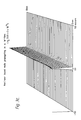
- Figures 3b and 3c show the profiles for higher launched power.
- the total energy must be conserved.
- the amount within a finite radius from the centre reduces, as energy is diffracted into the cladding.
- the energy confined within a 10 micron radius decreases much more slowly than for a fibre with no structure in the refractive index (the beam would disperse in a distance of about a millimetre in a homogeneous fibre).
- Figure 4 shows the fraction of the launched energy still confined within a 10 ⁇ m radius for fibres 7.5mm, 15mm and 30mm long as a function of n2.
- the fibre can be used as a threshold device. If the centre part of the beam were coupled into (say) a second standard monomode fibre then the fraction of the total energy launched into the propagating mode would depend on the input power.
- FIG. 5 An example of an assembly incorporating a W-profile fibre is shown in Figure 5.
- a W profile optical fibre 11 is connected to a Y coupler 12.
- One of the input arms 13 of the Y coupler 12 is coupled with a laser 14 while the output arm of the coupler 12 is connected to the fibre 11.
- a monomode optical fibre 15 is spliced to the central core of the fibre 11.
- a bias optical signal is supplied from the laser 14 to the optical fibre 11.
- the intensity of the bias signal is selected to lie on the portion of the transmission power profile ( Figure 4) close to the step part of the profile. For example, for a 30 mm optical fibre, the bias intensity will be chosen to lie at about the position 16.
- a small control signal applied along the other input arm 17 of the Y coupler 12 will cause the total incident intensity to lie at a position towards the top of the graph shown in Figure 4 resulting in a relatively high output power.
- the transverse form of the bias signal alone will be similar to that of Figure 3a.
- the energy is spread over a large area with a very small proportion within the central core region so that only a very small amount of the signal is coupled into the optical fibre 15.
- a signal is supplied along the arm 17, this adds to the intensity of the bias signal to such an extent that the total intensity changes to, for example, the position 18 in Figure 4.
- This causes the optical fibre 11 to switch into its self-guiding mode in which a large proportion of the initial total intensity is guided within the core to the output end of the fibre as shown in Figure 3c.
- a large intensity signal is coupled into the optical fibre 15.
- the optical fibre 11 could be used as an AND circuit with two input signals being fed along the arms 13, 17 (laser 14 being omitted) so that only when signals of sufficient intensity are fed along both the arms 13, 17 is there sufficient intensity from the resultant signal for self-guiding to produce a large output power within the central core of the optical fibre 11.
Landscapes
- Physics & Mathematics (AREA)
- Nonlinear Science (AREA)
- General Physics & Mathematics (AREA)
- Optics & Photonics (AREA)
- Optical Integrated Circuits (AREA)
- Glass Compositions (AREA)
- Optical Couplings Of Light Guides (AREA)
- Surgical Instruments (AREA)
- Laser Surgery Devices (AREA)
- Optical Communication System (AREA)
Claims (11)
- Optische Vorrichtung mit
einem optischen Wellenleiter (11), der gebildet ist aus einer Anordnung von optisch leitenden Medien mit unterschiedlichen Brechungsindizes, von denen mindestens einer nichtlinear ist in dem Sinn, daß sein Brechungsindex mit der Intensität des eingegebenen Lichts variiert, wobei ein optisches Signal mit einer einzigen Mode entlang dem Wellenleiter geleitet wird oder nicht in Übereinstimmung mit der Intensität des optischen Signals;
einer Kopplungseinrichtung (12) einschließlich Eingabeeinrichtungen (13, 17) zum Koppeln des optischen Signals in ein Eingabeende des Wellenleiters;
und einer Trennungseinrichtung (15), die einem Ausgabeende des Wellenleiters zugeordnet ist zum Trennen der geleiteten Anteile des optischen Signals von den nicht geleiteten Anteilen da Signals;
wobei die optische Vorrichtung dadurch gekennzeichnet ist, daß
die optische Eingabeeinrichtung eine erste (13) und eine zweite (17) Eingabeeinrichtung enthält zum Koppeln eines ersten und zweiten optischen Signals in den Wellenleiter, wobei die kombinierte Intensität der angelegten optischen Signale bestimmt, ob eine Signalmoden-Leitung stattfindet oder nicht. - Vorrichtung nach Anspruch 1, wobei die Trennungseinrichtung eine optische Monomoden-Faser (15) aufweist.
- Vorrichtung nach einem der vorhergehenden Ansprüche, wobei der Wellenleiter (11) zumindest drei ineinander verschachtelte Medien aufweist, wobei die beiden inneren Medien Brechungsindizes in dem leitenden Zustand haben, und jeweils größer bzw. kleiner als der Brechungsindex des äußeren Mediums, wobei der Brechungsindex von zumindest einem der inneren Medien nichtlinear ist.
- Vorrichtung nach Anspruch 3, wobei der Wellenleiter (11) einen Kern, eine innere den Kern umgebende Plattierung und eine äußre die innere Plattierung umgebende Plattierung aufweist.
- Vorrichtung nach einem der vorhergehenden Ansprüche, wobei der Wellenleiter (11) eine optische Faser aufweist.
- Vorrichtung nach Anspruch 5, wenn sie von Anspruch 4 abhängt, wobei die den Wellenleiter aufweisende optische Faser einen W-Profil-Brechungsindex hat.
- Vorrichtung nach einem der vorhergehenden Ansprüche, wobei alle Medien nichtlinear sind.
- Vorrichtung nach einem der vorhergehenden Ansprüche, welche weiterhin eine Vorspannungssignal-Erzeuguneinrichtung aufweist, die im Betrieb mit der Kopplungseinrichtung zum Injizieren eines optischen Vorspannungssignals in das Eingabeende des Wellenleiters verbunden ist, wobei die Intensität des Vorspannungssignals derart ist, daß der Wellenleiter in seinem nichtlinearen Bereich arbeitet und das Vorspannungssignal abgeschnitten wird.
- Vorrichtung nach einem der vorhergehenden Ansprüche, wobei die Kopplungseinrichtung einen Y-Koppler (12) aufweist, wobei ein Eingabearm des Kopplers mit der Vorspannungssignal-Erzeugungseinrichtung (13), der andere Eingabearm des Kopplers (17) mit einem Eingabesignal und der Ausgabearm des Kopplers (12) mit dem Wellenleiter (11) gekoppelt ist.
- Optischer Schalter einschließlich einer optischen Vorrichtung gemäß einem der vorhergehenden Ansprüche.
- Verfahren zum Betreiben einer optischen Vorrichtung gemäß einem der vorhergehenden Ansprüche, wobei das Verfahren dadurch gekennzeichnet ist, daß es die folgenden Schritte aufweist: Injizieren eines ersten optischen Signals in den Wellenleite, wobei die Intensität des ersten Signals derart ist, daß das Signal im wesentlichen abgeschnitten wird; und Injizieren eines zweiten optischen Signals in den Wellenleiter mit einer derartigen Intensität, daß die Resultierende des ersten und zweiten Signals eine ausreichende Intensität hat, um durch den Wellenleiter geleitet zu werden.
Priority Applications (1)
| Application Number | Priority Date | Filing Date | Title |
|---|---|---|---|
| AT87308107T ATE80231T1 (de) | 1986-09-16 | 1987-09-14 | Optische vorrichtung. |
Applications Claiming Priority (2)
| Application Number | Priority Date | Filing Date | Title |
|---|---|---|---|
| GB8622314 | 1986-09-16 | ||
| GB868622314A GB8622314D0 (en) | 1986-09-16 | 1986-09-16 | Optical device |
Publications (2)
| Publication Number | Publication Date |
|---|---|
| EP0263604A1 EP0263604A1 (de) | 1988-04-13 |
| EP0263604B1 true EP0263604B1 (de) | 1992-09-02 |
Family
ID=10604280
Family Applications (1)
| Application Number | Title | Priority Date | Filing Date |
|---|---|---|---|
| EP87308107A Expired - Lifetime EP0263604B1 (de) | 1986-09-16 | 1987-09-14 | Optische Vorrichtung |
Country Status (8)
| Country | Link |
|---|---|
| US (1) | US4938557A (de) |
| EP (1) | EP0263604B1 (de) |
| JP (1) | JPH0721601B2 (de) |
| AT (1) | ATE80231T1 (de) |
| CA (1) | CA1295156C (de) |
| DE (1) | DE3781498T2 (de) |
| GB (1) | GB8622314D0 (de) |
| WO (1) | WO1988002132A1 (de) |
Families Citing this family (11)
| Publication number | Priority date | Publication date | Assignee | Title |
|---|---|---|---|---|
| JPH0279029A (ja) * | 1988-09-16 | 1990-03-19 | Nippon Telegr & Teleph Corp <Ntt> | 非線形光学装置 |
| US4932739A (en) * | 1989-09-25 | 1990-06-12 | At&T Bell Laboratories | Ultra-fast optical logic devices |
| US5711884A (en) * | 1990-08-22 | 1998-01-27 | University Of Pittsburgh Of The Commonwealth System Of Higher Education | Method of filtering submicron particles with gel lattice membrane filter |
| US5448664A (en) * | 1992-12-11 | 1995-09-05 | Alexander Shkolnik | Optical gates where output signal intensity is independent of phases of input signals |
| US5452123A (en) * | 1992-12-30 | 1995-09-19 | University Of Pittsburgh Of The Commonwealth System Of Higher Education | Method of making an optically nonlinear switched optical device and related devices |
| US5737102A (en) * | 1992-12-30 | 1998-04-07 | University Of Pittsburgh Of The Commonwealth System Of Higher Education | Method of making an optically nonlinear switched optical device and related devices |
| WO1996005605A1 (en) * | 1994-08-15 | 1996-02-22 | Nigel Eric Rose | Improvements to switching systems |
| WO1996028758A1 (en) * | 1995-03-15 | 1996-09-19 | Philips Electronics N.V. | Optical switch |
| US6014246A (en) * | 1996-11-06 | 2000-01-11 | University Of Pittsburgh Of The Commonwealth System Of Higher Education | Thermally switchable optical devices |
| WO2001063345A2 (en) | 2000-02-23 | 2001-08-30 | University Of Pittsburgh Of The Commonwealth System Of Higher Education | Photochemically controlled photonic crystal diffraction |
| CN102216822B (zh) * | 2011-05-09 | 2013-01-09 | 华为技术有限公司 | 无源光分路器和无源光网络系统 |
Family Cites Families (2)
| Publication number | Priority date | Publication date | Assignee | Title |
|---|---|---|---|---|
| US4515429A (en) * | 1980-05-27 | 1985-05-07 | At&T Bell Laboratories | Nonlinear and bistable optical waveguide devices |
| JPS6197630A (ja) * | 1984-10-18 | 1986-05-16 | Nippon Telegr & Teleph Corp <Ntt> | 光フアイバ論理素子 |
-
1986
- 1986-09-16 GB GB868622314A patent/GB8622314D0/en active Pending
-
1987
- 1987-09-14 US US07/193,285 patent/US4938557A/en not_active Expired - Lifetime
- 1987-09-14 WO PCT/GB1987/000639 patent/WO1988002132A1/en not_active Ceased
- 1987-09-14 DE DE8787308107T patent/DE3781498T2/de not_active Expired - Fee Related
- 1987-09-14 JP JP62505538A patent/JPH0721601B2/ja not_active Expired - Lifetime
- 1987-09-14 AT AT87308107T patent/ATE80231T1/de not_active IP Right Cessation
- 1987-09-14 EP EP87308107A patent/EP0263604B1/de not_active Expired - Lifetime
- 1987-09-15 CA CA000546917A patent/CA1295156C/en not_active Expired - Lifetime
Also Published As
| Publication number | Publication date |
|---|---|
| EP0263604A1 (de) | 1988-04-13 |
| JPH0721601B2 (ja) | 1995-03-08 |
| ATE80231T1 (de) | 1992-09-15 |
| WO1988002132A1 (en) | 1988-03-24 |
| JPH01500858A (ja) | 1989-03-23 |
| DE3781498T2 (de) | 1993-01-07 |
| DE3781498D1 (de) | 1992-10-08 |
| US4938557A (en) | 1990-07-03 |
| GB8622314D0 (en) | 1986-10-22 |
| CA1295156C (en) | 1992-02-04 |
Similar Documents
| Publication | Publication Date | Title |
|---|---|---|
| EP0265233B1 (de) | Nicht-lineare, optische Vorrichtung | |
| US6011881A (en) | Fiber-optic tunable filter | |
| US4913507A (en) | Mode field conditioner | |
| Stegeman et al. | Nonlinear organic materials in integrated optics structures | |
| US4938557A (en) | Optical device | |
| US6269205B1 (en) | Optical devices based on energy transfer between different modes in optical waveguide | |
| US20200225415A1 (en) | Resonance-free light recycling in waveguides | |
| Meng et al. | Improved coupled-mode theory for nonlinear directional couplers | |
| Menéndez | Fiber-Optic Ring Resonator | |
| Winful et al. | Applications of nonlinear periodic structures in guided wave optics | |
| Shi | Optical bistability in reflective fiber gratings | |
| Sanchez | Optical bistability in a 2× 2 coupler fiber ring resonator: parametric formulation | |
| Bahadoran et al. | Realizing unique bifurcation model in a cascaded microring feedback circuit | |
| Kaczmarski et al. | Design of an integrated electro-optic switch in organic polymers | |
| JPH11507741A (ja) | マッハ・ツェンダ・スイッチ | |
| Ogusu | Self-switching in hollow waveguides with a Kerrlike nonlinear permittivity | |
| Francois et al. | Multimode nature of quadruple-clad fibres | |
| Dinleyici et al. | Calculation of the wavelength filter properties of the fiber-slab waveguide structure using vector mode expansion | |
| Blow et al. | Nonlinear self-guiding and switching in an all-fiber device | |
| Khalil et al. | Asymmetric excitation of symmetric single-mode Y-junctions: the radiation mode effects | |
| Lee et al. | Observation of enhanced group velocity dispersion in coupled waveguide structures | |
| Vassilopoulos et al. | Backward wave couplers and reflectors | |
| Giles et al. | Integrated all-fibre VOA: power monitor module for fibre channel power control using a novel fibre substrate approach | |
| Lederer et al. | Linear mode beating and nonlinear mode coupling in resonant optical waveguides | |
| Khalil et al. | Novel structure for electro-optic intensity modulators: the radiation mode modulator |
Legal Events
| Date | Code | Title | Description |
|---|---|---|---|
| PUAI | Public reference made under article 153(3) epc to a published international application that has entered the european phase |
Free format text: ORIGINAL CODE: 0009012 |
|
| AK | Designated contracting states |
Kind code of ref document: A1 Designated state(s): AT BE CH DE ES FR GB GR IT LI LU NL SE |
|
| 17P | Request for examination filed |
Effective date: 19881012 |
|
| RAP3 | Party data changed (applicant data changed or rights of an application transferred) |
Owner name: BRITISH TELECOMMUNICATIONS PUBLIC LIMITED COMPANY |
|
| 17Q | First examination report despatched |
Effective date: 19901206 |
|
| GRAA | (expected) grant |
Free format text: ORIGINAL CODE: 0009210 |
|
| AK | Designated contracting states |
Kind code of ref document: B1 Designated state(s): AT BE CH DE ES FR GB GR IT LI LU NL SE |
|
| PG25 | Lapsed in a contracting state [announced via postgrant information from national office to epo] |
Ref country code: GR Free format text: LAPSE BECAUSE OF FAILURE TO SUBMIT A TRANSLATION OF THE DESCRIPTION OR TO PAY THE FEE WITHIN THE PRESCRIBED TIME-LIMIT Effective date: 19920902 Ref country code: AT Effective date: 19920902 |
|
| REF | Corresponds to: |
Ref document number: 80231 Country of ref document: AT Date of ref document: 19920915 Kind code of ref document: T |
|
| PG25 | Lapsed in a contracting state [announced via postgrant information from national office to epo] |
Ref country code: LU Free format text: LAPSE BECAUSE OF NON-PAYMENT OF DUE FEES Effective date: 19920930 |
|
| REF | Corresponds to: |
Ref document number: 3781498 Country of ref document: DE Date of ref document: 19921008 |
|
| ITF | It: translation for a ep patent filed | ||
| ET | Fr: translation filed | ||
| PG25 | Lapsed in a contracting state [announced via postgrant information from national office to epo] |
Ref country code: ES Free format text: LAPSE BECAUSE OF FAILURE TO SUBMIT A TRANSLATION OF THE DESCRIPTION OR TO PAY THE FEE WITHIN THE PRESCRIBED TIME-LIMIT Effective date: 19921213 |
|
| PLBE | No opposition filed within time limit |
Free format text: ORIGINAL CODE: 0009261 |
|
| STAA | Information on the status of an ep patent application or granted ep patent |
Free format text: STATUS: NO OPPOSITION FILED WITHIN TIME LIMIT |
|
| 26N | No opposition filed | ||
| EAL | Se: european patent in force in sweden |
Ref document number: 87308107.9 |
|
| PGFP | Annual fee paid to national office [announced via postgrant information from national office to epo] |
Ref country code: FR Payment date: 19980810 Year of fee payment: 12 |
|
| PGFP | Annual fee paid to national office [announced via postgrant information from national office to epo] |
Ref country code: SE Payment date: 19980813 Year of fee payment: 12 |
|
| PGFP | Annual fee paid to national office [announced via postgrant information from national office to epo] |
Ref country code: NL Payment date: 19980819 Year of fee payment: 12 |
|
| PGFP | Annual fee paid to national office [announced via postgrant information from national office to epo] |
Ref country code: DE Payment date: 19980826 Year of fee payment: 12 |
|
| PGFP | Annual fee paid to national office [announced via postgrant information from national office to epo] |
Ref country code: CH Payment date: 19980827 Year of fee payment: 12 |
|
| PGFP | Annual fee paid to national office [announced via postgrant information from national office to epo] |
Ref country code: BE Payment date: 19980904 Year of fee payment: 12 |
|
| PG25 | Lapsed in a contracting state [announced via postgrant information from national office to epo] |
Ref country code: SE Free format text: THE PATENT HAS BEEN ANNULLED BY A DECISION OF A NATIONAL AUTHORITY Effective date: 19990929 |
|
| PG25 | Lapsed in a contracting state [announced via postgrant information from national office to epo] |
Ref country code: LI Free format text: LAPSE BECAUSE OF NON-PAYMENT OF DUE FEES Effective date: 19990930 Ref country code: CH Free format text: LAPSE BECAUSE OF NON-PAYMENT OF DUE FEES Effective date: 19990930 Ref country code: BE Free format text: LAPSE BECAUSE OF NON-PAYMENT OF DUE FEES Effective date: 19990930 |
|
| BERE | Be: lapsed |
Owner name: BRITISH TELECOMMUNICATIONS P.L.C. Effective date: 19990930 |
|
| PG25 | Lapsed in a contracting state [announced via postgrant information from national office to epo] |
Ref country code: NL Free format text: LAPSE BECAUSE OF NON-PAYMENT OF DUE FEES Effective date: 20000401 |
|
| EUG | Se: european patent has lapsed |
Ref document number: 87308107.9 |
|
| REG | Reference to a national code |
Ref country code: CH Ref legal event code: PL |
|
| PG25 | Lapsed in a contracting state [announced via postgrant information from national office to epo] |
Ref country code: FR Free format text: LAPSE BECAUSE OF NON-PAYMENT OF DUE FEES Effective date: 20000531 |
|
| NLV4 | Nl: lapsed or anulled due to non-payment of the annual fee |
Effective date: 20000401 |
|
| REG | Reference to a national code |
Ref country code: GB Ref legal event code: 732E |
|
| PG25 | Lapsed in a contracting state [announced via postgrant information from national office to epo] |
Ref country code: DE Free format text: LAPSE BECAUSE OF NON-PAYMENT OF DUE FEES Effective date: 20000701 |
|
| REG | Reference to a national code |
Ref country code: FR Ref legal event code: ST |
|
| PGFP | Annual fee paid to national office [announced via postgrant information from national office to epo] |
Ref country code: GB Payment date: 20010817 Year of fee payment: 15 |
|
| REG | Reference to a national code |
Ref country code: GB Ref legal event code: IF02 |
|
| PG25 | Lapsed in a contracting state [announced via postgrant information from national office to epo] |
Ref country code: GB Free format text: LAPSE BECAUSE OF NON-PAYMENT OF DUE FEES Effective date: 20020914 |
|
| GBPC | Gb: european patent ceased through non-payment of renewal fee |
Effective date: 20020914 |
|
| PG25 | Lapsed in a contracting state [announced via postgrant information from national office to epo] |
Ref country code: IT Free format text: LAPSE BECAUSE OF NON-PAYMENT OF DUE FEES;WARNING: LAPSES OF ITALIAN PATENTS WITH EFFECTIVE DATE BEFORE 2007 MAY HAVE OCCURRED AT ANY TIME BEFORE 2007. THE CORRECT EFFECTIVE DATE MAY BE DIFFERENT FROM THE ONE RECORDED. Effective date: 20050914 |